
 Open Access Article
 This Open Access Article is licensed under a Creative Commons Attribution-Non Commercial 3.0 Unported Licence
Gigantic enhancement of optoelectrical properties in polythiophene thin films via MoS2 nanosheet-induced aggregation and ordering
Mitu
Chauhan
 a,
Anand Kumar
Singh
b,
Vivek
Chaudhary
c,
Rajiv Kumar
Pandey
d and
Arun Kumar
Singh
*a
a,
Anand Kumar
Singh
b,
Vivek
Chaudhary
c,
Rajiv Kumar
Pandey
d and
Arun Kumar
Singh
*a
aDepartment of Pure and Applied Physics, Guru Ghasidas Vishwavidyalaya, Bilaspur (C.G.)-495009, India. E-mail: arunsingh.itbhu@gmail.com
bSchool of Engineering and Technology, Vivekananda Institute of Professional Studies-Technical Campus (VIPS-TC), Pitampura, New Delhi-110034, India
cSchool of Applied and Engineering Physics, Mohammed VI Polytechnic University, Ben Guerir, 43150, Morocco
dSKKU Advanced Institute of Nanotechnology, Sungkyunkwan University, Suwon 16419, South Korea
First published on 7th February 2025
Abstract
Conducting polymers (CPs), such as poly(3,3-dialkylquarterthiophene) (PQT-12), are attractive candidates for flexible thin-film electronics due to their cost-effectiveness and mechanical flexibility. However, the industrial application of CPs is limited by poor crystallinity and disordered polymer chain orientation. Herein, we report the enhancement in optical, structural, and electronic properties of PQT-12 by incorporating MoS2 nanosheets in the polymer matrix. The PQT-12/MoS2 nanocomposite exhibits improved crystallinity, molecular ordering, and charge transport properties, as evidenced by enhanced UV-visible absorption, quenched photoluminescence, and increased coherence length in X-ray diffraction. The floating-film transfer method (FTM), a scalable technique for large-area film fabrication has been used for thin film deposition. The nanocomposite film reveals a more ordered nano-fibrillar network in atomic force microscopy images, which is crucial for efficient charge transport. The charge transport has been studied by fabricating organic field-effect transistors (OFETs) and Schottky diodes. The nanocomposite based OFETs have shown mobility up to 3.6 × 10⁻³ cm V−1 s−1 with an on/off ratio of 104, while Schottky diodes exhibit enhanced ideality factor, rectification ratio, and barrier height. These improvements are attributed to charge transfer interactions and enhanced polymer chain alignment induced by MoS2 nanosheets, demonstrating their potential for high-performance flexible electronics.
1. Introduction
Solution-processable conducting polymers (CPs) are increasingly being considered for the cost-effective production of flexible thin-film electronic devices used in many technological applications due to their ease of use and inherent flexibility.1 The solution processability, cost-effectiveness, and flexibility of CPs make them exceptionally better than other semiconductors (e.g., conventional semiconductors, oxide semiconductors, perovskites, and low-dimensional semiconductors), which can enable the fabrication of more complex devices. Many organic electronic devices, including organic Schottky diodes (OSDs),1–3 organic light emitting diodes,4,5 organic field effect transistors (OFETs),6 and organic solar cells,7 flexible information displays,8 electronic skin,9 digital healthcare monitoring,8 brain signal recording,10 and supercapacitors11 have been demonstrated. The development of organic thin-film electronic devices is currently underway; however, the poor crystallinity and random orientations of the polymer chains limit their performance. The performance of these electronic devices very strongly depends on intermolecular and intramolecular interactions, molecular alignment, crystallinity, and the interface properties of CPs.5,12,13 Therefore, it is necessary to control the inter/intramolecular interactions, surface morphology, and orientation of the polymer chains for enhancing the performance of electronic devices.Among CPs, polythiophenes have become the benchmark polymer semiconductor materials for electronic devices. The solution-processable derivative of polythiophene, poly(3,3′′′-dialkylquarterthiophene) (PQT-12), has attracted wide scientific interest due to its ability to self-assemble, better air stability, and superior charge transport characteristics than other polymers of the thiophene family.14–17 The interchain stacking and intermolecular interdigitation through alkyl side chains can tune the charge transport properties of PQT-12. The alkyl side chains of PQT-12 not only provide additional ordering but also improve their solubility in common organic solvents. The effect of chain orientation, π–π stacking, alkyl side-chain interactions, and molecular weight-dependent chain ordering on overall device performance has been explained well and presented in several existing studies.18 Solvent-evaporation dependent crystallization kinetics and aggregated structures in films of PQT-12 have also been demonstrated previously.19 Thus, there is a need for a cautious optimization of the film fabrication. Thin-film fabrication via solution-state self-assembly is a vital approach for future organic-semiconductor based electronic devices because the performance of these devices mainly depends on the aggregation and alignment of the polymer chains in the thin film.
In recent years, two-dimensional (2D) nanomaterials have attracted enormous attention because they provide remarkable tuning of structural, optical and optoelectronic properties. Molybdenum disulfide (MoS2) is one of the most explored transition metal dichalcogenides (TMDCs) and is well-known for exhibiting layer dependent electronic and optical properties; making it potentially useful in next-generation nanoelectronics.20 MoS2-based FETs have recently attracted a lot of interest for several applications, including photoelectrical detectors, gas sensors, and ultra-thin integrated circuits.21,22 The MoS2 nanosheets in CPs/MoS2 nanohybrids provide interconnected pathways that result in highly efficient long-range charge transport and improved carrier hopping along the π–π stacking direction in organic electronic devices, which is highly necessary for planar devices. But the exact nature of charge-transfer interactions between the conducting polymer and MoS2 still needs to be understood.23–25 To the best of our knowledge the structural, optical and electrical properties along with the nature and mechanism of interaction involved between the PQT-12 polymer and MoS2 have not yet been reported.
In this study, we have investigated the self-assembly and ordering of PQT-12 chains in thin films mediated by MoS2 nanosheets. The floating film transfer (FTM) method is used to deposit homogeneous, large-area, and high-quality films. The PQT-12/MoS2 nanocomposite films exhibit significantly enhanced photophysical and charge transport properties compared to pristine PQT-12. The absorption and emission spectra, along with the atomic force microscopy (AFM) images, indicate improvements in optical and morphological properties. Incorporating MoS2 flakes into the polymer matrix introduces novel electronic interactions, enhancing crystallinity, polymer chain length, and network connectivity, resulting in more efficient charge carrier transport pathways. We also report a significant improvement in charge carrier mobility and on/off ratio for the nanocomposite films, along with a reduction in charge trap density. Additionally, we fabricated organic Schottky diodes using the configuration Al/PQT-12/MoS2/ITO and analyzed their current density–voltage characteristics, comparing them with pristine PQT-12 diodes to understand the conduction mechanism at the metal-semiconductor interface.
2. Experimental details
2.1. Synthesis of the nanocomposites and film formation
PQT-12 is purchased from the American Dye Source, Inc., USA, and used in our study without any additional refining. MoS2 crystals were purchased from SPI supplies, USA, and other chemicals were purchased from Sigma-Aldrich. Before preparing the PQT-12/MoS2 nanocomposite, 1 mg of MoS2 flakes were exfoliated in anhydrous chloroform via sonication for 5 h at 30 kHz similar to as discussed in our previous reports.23 30 μL of exfoliated MoS2 nanosheet solution was added dropwise to 3 mg PQT-12 in 970 μL anhydrous chloroform in glass vials to prepare the concentration 1 wt% MoS2 in PQT-12. This 1 wt% concentration of MoS2 was chosen according to our previous work.23 During dropwise addition of MoS2 nanosheets in PQT-12, 15 min of sonication was performed in each step. The prepared solution was finally sonicated for 3 h approximately at 5–10 °C before the use of the solutions for the formation of thin films. The preparation of the PQT-12/MoS2 nanocomposite is schematically shown in Fig. 1(a).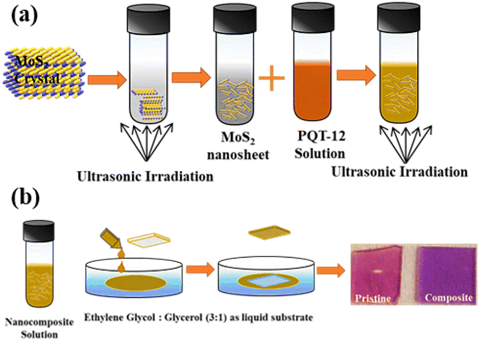 | ||
| Fig. 1 (a) Synthesis mechanism of PQT-12/MoS2 nanocomposite. (b) Schematic diagram of thin film formation by floating film transfer method and optical image of prepared films over glass substrate. | ||
For the formation of oriented and smooth thin films over the substrates (glass and SiO2/Si), we used 1![[thin space (1/6-em)]](https://www.rsc.org/images/entities/char_2009.gif) :3 mixtures of glycerol and ethylene glycol as the liquid substrate. 10 μL of PQT-12/MoS2 solution was dropped onto the liquid substrate for the formation of a thin film of PQT-12/MoS2 nanocomposite at the air–liquid interface. The detailed mechanism of the formation of the thin film over the liquid substrate is discussed elsewhere.23,26–28 The compact thin films were transferred over the glass, ITO coated glass and SiO2/Si substrates via horizontal stamping, as depicted in Fig. 1(b). For comparison purpose, we also prepared a thin film of pristine PQT-12 the same as the formation of thin films of the nanocomposite.
:3 mixtures of glycerol and ethylene glycol as the liquid substrate. 10 μL of PQT-12/MoS2 solution was dropped onto the liquid substrate for the formation of a thin film of PQT-12/MoS2 nanocomposite at the air–liquid interface. The detailed mechanism of the formation of the thin film over the liquid substrate is discussed elsewhere.23,26–28 The compact thin films were transferred over the glass, ITO coated glass and SiO2/Si substrates via horizontal stamping, as depicted in Fig. 1(b). For comparison purpose, we also prepared a thin film of pristine PQT-12 the same as the formation of thin films of the nanocomposite.
2.2. Characterizations and device fabrication
The UV-Vis absorption spectra of PQT-12 and PQT-12/MoS2 solutions and thin films on a glass substrate were recorded in the range from 300 nm to 800 nm using a dual-beam spectrophotometer (PerkinElmer Lambda 25, Germany) to determine the effect of MoS2 nanosheets on aggregation and ordering. The photoluminescence emission spectrum of the sample was recorded using a Cary Eclipse Spectrophotometer. The structural characterization of the PQT-12 and PQT-12/MoS2 films was carried out by using the grazing incidence X-ray diffraction (GIXD) measurement (Rigaku smart lab system, thin film XRD) equipped with an in-plane diffractometer at a 0.2° grazing angle. The surface morphology and thickness of the pristine PQT-12 and PQT-12/MoS2 films coated on the SiO2/Si substrate were measured by using an AFM (NT-MDT, Russia, model PRO 47) operating in tapping mode. The thickness of the film was found to be 20 ± 2 nm in all cases. To examine the MoS2 nanosheets and distribution of MoS2 in the polymer matrix, transmission electron microscopy (TEM) (FEI, Tech G2 New Zealand) was employed. To measure the charge transport properties of PQT-12 and PQT-12/MoS2 films, we fabricated both diodes and transistors. For diode fabrication, first we transferred PQT-12 and PQT-12/MoS2 thin films over a pre-patterned ITO substrate, the same as discussed above. The 90 nm aluminum (Al) top electrodes were deposited via thermal vacuum evaporation (HIND HIVAC model 12A4D) on PQT-12 and PQT-12/MoS2 thin film coated ITO substrates through a shadow mask keeping the active area for the devices at 1 × 1 mm2. All the ITO and SiO2/Si (heavily p-doped Si) substrates were cleaned using the standard method before device fabrication. The SiO2 (300 nm)/Si substrate treated with octyltrichlorosilane (OTS) in toluene is used as a gate dielectric and has a capacitance equal to 10 nF cm−2.29 The gold (Au) source-drain electrodes of thickness 30 nm were deposited by a thermal evaporating system (HIND HIVAC model 12A4D) with a nickel mask that has 50 μm channel length and 2 mm channel width. Finally, the electrical transport properties of all samples are investigated using the Keysight parameter analyzer (B1500A) in ambient conditions.3. Results and discussion
Fig. 2(a) and (b) display the UV-Vis absorption spectra of pristine PQT-12 and the PQT-12/MoS2 nanocomposite respectively in solution and the thin-film state. In solution form, the strong absorption peak at 450 nm corresponds to π–π* transition that stems from strong conjugation in the PQT-12 backbone. A notable bathochromic shift is observed in the absorption peaks of the PQT-12 and PQT-12/MoS2 nanocomposite thin films. This shift is attributed to increased interchain interactions and changes in molecular polarity caused by evaporation of the polar solvent environment. Additionally, the formation of the film on a liquid substrate introduces a directional alignment and extended crystalline domains, which further contributes to the red shift.30 In thin films, the UV-vis spectra of both pristine PQT-12 and PQT-12/MoS2 reveal three distinct absorption peaks at 502, 541, and 579 nm, which correspond to A0–2, A0–1, and A0–0 transitions, respectively. The peaks at 541 and 579 nm are more pronounced in the PQT-12/MoS2 films compared to the pristine PQT-12 films. These peaks are associated with the ordered coplanar orientation of the conjugated chain and alignment of the side chains due to incorporation of MoS2 bridging among the polymer chains enhancing π–π stacking.14,31,32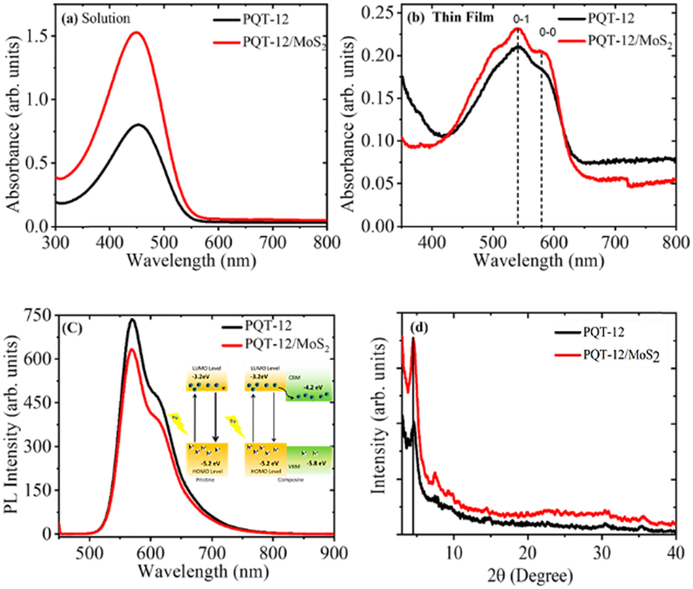 | ||
| Fig. 2 UV-vis absorption spectra of pristine PQT-12 and PQT-12/MoS2 (a) solution and (b) thin films. (c) Photoluminescence spectra of the pristine PQT-12 and PQT-12/MoS2 nanocomposite solution. The figure inset shows the schematic band diagram. (d) XRD profiles of pristine PQT-12 and PQT-12/MoS2 films. | ||
Fig. 2(c) compares the photoluminescence (PL) emission spectra of PQT-12 and PQT-12/MoS2 nanocomposite solutions with an excitation wavelength of 500 nm. Both solutions show a strong PL band peaking at 570 nm with a small side hump at 611 nm arising from excitonic transitions of the conjugated core of PQT-12. The incorporation of MoS2 in PQT-12 shows a reduction in the PL intensity, which indicates the existence of non-radiative transitions in the nanocomposite system, which may arise from overlapping of the absorption band of MoS2 with the emission band of the polymer indicating the existence of a long rang electronic energy transfer process.33,34 Since the absorption spectra of MoS2 extend up to the near-infrared region with two direct excitonic bands, this opens up the possibility of electronic interaction between PQT-12 and MoS2.35 Hence, quenching of PL of the nanocomposite can be understood by the schematic representation of the band diagram in the inset of Fig. 2(c). The movement of excited electrons from the LUMO level of PQT-12 towards the conduction band of MoS2 due to favorable band alignment causes quenching in the PL spectra and reduces recombination of excitons in the HOMO level, which results in better electronic performance of the composite.
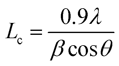
XRD of pristine PQT-12 and PQT-12/MoS2 thin films has been performed to examine the orientation, coherence length, and interplanar spacing. Pristine PQT-12 and PQT-12/MoS2 composite films have (100) diffraction peaks that appeared at 2θ angles of 4.648° and 4.560°, respectively, as shown in Fig. 2(d). The corresponding interlayer d-spacing (dh00) for the PQT-12 and PQT-12/MoS2 thin films is found to be 16.65 Å and 16.49 Å, respectively. The shrinkage of the interlayer distance in the PQT-12/MoS2 thin film indicates denser packing of atoms/molecules within the composite. This compactness causes more overlapping of the π electron wavefunction, which in turn enhances the delocalization of holes along the π–π stacking direction.23 It is due to the involvement of stronger binding forces in-between the molecules, which are discussed in detail in the later section. The thin films exhibit (h00) molecular stacking along the alkyl chain direction and normal to the substrate, which is suitable for in-plane electronic devices. However, a decrease in FWHM for the (100) reflection peak reflects an increase of coherence length from 10.7 nm in the pristine PQT-12 film to 12.8 nm in the nanocomposite film. Coherence length for the films is calculated by the Debye–Scherer relation:36
 | (1) |
The morphology of the polymer films is a critical factor in determining the device performance, as the degree of order and connectivity in the film surface can significantly enhance charge carrier transport. In the provided analysis, AFM was used to compare the surface topography of pure PQT-12 films and PQT-12/MoS2 nanocomposite films (Fig. 3(a) and (b)). The AFM topography of pure PQT-12 films reveals a very smooth and featureless surface. This indicates a lack of significant surface texture or microstructure, which may correlate with lower charge transport efficiency due to the absence of well-defined pathways. In contrast, the nanocomposite films (PQT-12 with MoS2) exhibit a globular surface structure. This distinct morphology is characterized by interconnected nanofibrillar networks, which suggest a more ordered packing of the polymer chains. The presence of MoS2 nanosheets is crucial here, as they serve as nucleation sites that promote the self-assembly of PQT-12 chains into nanofibers, likely through π–π stacking with a preferential edge-on orientation. Ahmad et al. reported similar morphological changes in a different polymer system (P3HT/MoS2), where the incorporation of MoS2 led to the formation of longer, more ordered polymeric fibers.31 These globular structures are interconnected nano-fibrillar networks, which are characteristics of ordered packaging.37,38 The phase imaging in their study also revealed a reduction in height and the emergence of a globular structure in tapping mode, akin to the findings for the PQT-12/MoS2 films. The change in morphology upon the addition of MoS2 is attributed to the large surface area of the MoS2 nanosheets, which act as nucleation centers for long range aggregation. The strong dipole–dipole interactions between the conjugated core of the polymer and the localized electron clouds of sulfur in MoS2 facilitate the aggregation process around the nanosheets. This leads to the formation of long polymer nanofibers and interconnected nanofibrillar networks. These networks not only enhance the order of the polymer chains, but also act as physical bridges between neighboring fibers, potentially improving intrinsic charge carrier transport and thus device performance.
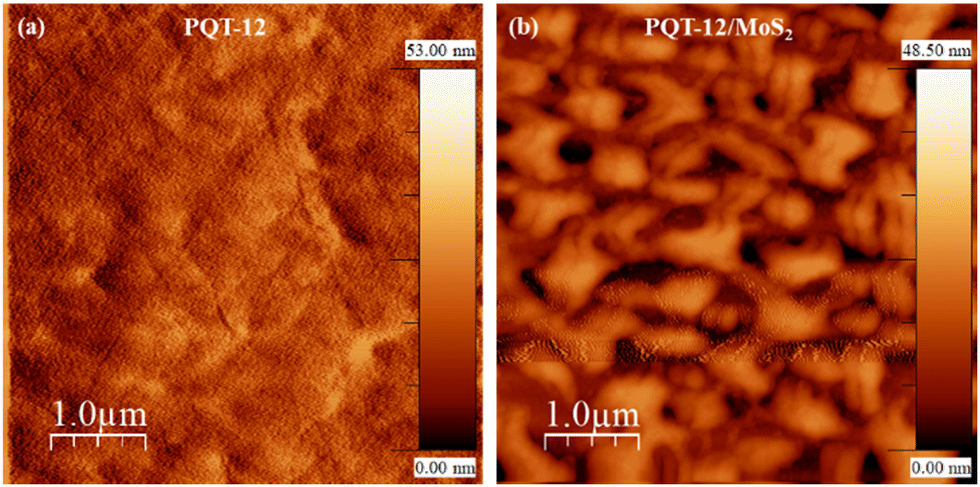 | ||
| Fig. 3 AFM phase images of (a) pristine PQT-12 and (b) PQT-12/MoS2 films. | ||
The 2D MoS2 nanosheets are successfully obtained by the liquid-phase exfoliation method. The TEM image of 2D MoS2 nanosheets is shown in Fig. 4(a), which shows ultrathin layers with lateral dimensions across hundreds of nanometers. Fig. 4(b) depicts high-resolution TEM images of the obtained nano-sheets with crystal lattice fringes of 0.28 nm assigned mainly to the (001) planes of MoS2, which revealed the mono- or few-layer of MoS2.26 The inset of Fig. 4(b) shows the selected area electron diffraction (SAED) pattern of the MoS2 nanosheets; it attributes the hexagonal diffraction pattern of the spots and highly crystalline nature. Fig. 4(c) shows the TEM image of the PQT-12/MoS2 nanocomposite, which clearly revealed that MoS2 nanosheets are covered by PQT-12 polymer chains as well as uniformly distributed in the polymer matrix. HRTEM images of the PQT-12/MoS2 nanocomposite demonstrate the fringe spacing of 0.36 nm corresponding to the (0k0) plane, revealing the edge-on orientation of the film, as shown in Fig. 4(d). The SAED pattern of the PQT-12/MoS2 nanocomposite shows several rings with different intensities that reveal the different periodicities of the structures and high crystallinity.
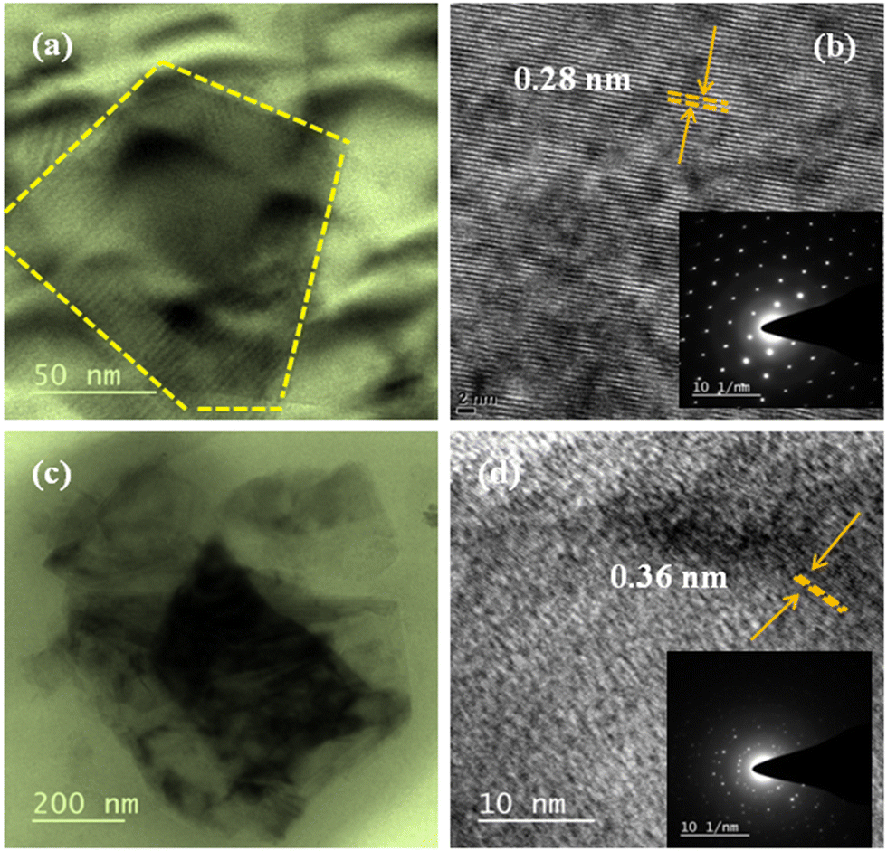 | ||
| Fig. 4 (a) TEM image of MoS2 nanosheets represented by the yellow dotted line. (b) HR-TEM of 2D MoS2 nanosheets showing the lattice fringes and inset displaying the SAED pattern of the MoS2 nanosheets. (c) TEM image of MoS2 nanosheets in the PQT-12 matrix. (d) HRTEM images of PQT-12/MoS2 and inset showing the SAED pattern of the PQT-12/MoS2. | ||
The interaction between the 2D layered material MoS2 and the organic polymer can be further elucidated by the schematic diagram in Fig. 5. In this diagram, the layered crystal structure of MoS2 is depicted, where molybdenum atoms are sandwiched between two sulfur atoms within each MoS2 layer. The layered structure allows sulfur atoms, which possess lone electron pairs, to generate an electron cloud on the outer surface of the layers. This electron cloud interacts with the conjugated backbone of the polymer via electrostatic interactions, significantly influencing the morphological, electrical, and optical properties of the conjugated polymer. The interaction between the outer electron cloud of the MoS2 layer and the aromatic ring of the polymer leads to the formation of a globular structure, as observed in the AFM image of the nanocomposite. This interaction creates a stronger attractive force compared to the typical dipole–dipole interactions or van der Waals forces. Consequently, more polymer chains are drawn towards the MoS2 nanosheets, resulting in the emergence of globular patch-like structures. These patches are indicative of longer and more aligned polymer chains in the nanocomposite, as supported by previous studies.37 The increased coherence length in the nanocomposite, evidenced by XRD analysis, further supports the notion of enhanced alignment and order within the polymer chains. Additionally, XRD and UV-visible absorption spectra confirm the enhanced crystallinity, denser packing, and more aligned orientation of the polymer chains, all of which are attributed to the interaction between the MoS2 and polymer chains. These morphological changes are crucial as they suggest the creation of more efficient pathways for charge transport, reduced resistance, and an overall increase in mobility.39 According to Mott's variable-range hopping conduction mechanism and percolation theory, efficient charge transport in materials is governed by the availability of multiple conducting channels. In hybrid materials like the polymer/MoS2 nanocomposite, the existence of multiple pathways for charge carrier transport is crucial. The crystalline and self-assembled polymer chains, which are interconnected via MoS2 nanosheets, acting as the most efficient channels for charge transport. This interconnection not only facilitates better charge mobility, but also enhances the overall performance of the material in electronic devices.
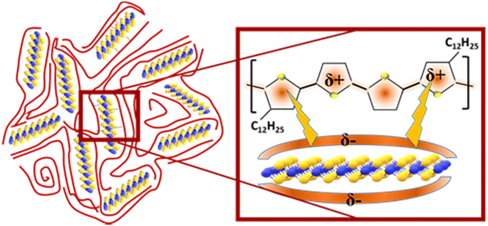 | ||
| Fig. 5 Schematic representation of intermolecular interaction between PQT-12 and MoS2 nanosheets. | ||
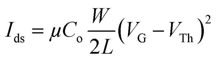
The enhanced crystallinity and improved morphology of the PQT-12/MoS2 nanocomposite film motivated an in-depth investigation of its electrical and charge transport properties, both along the film plane (in-plane) and across the film (out-of-plane), using organic field-effect transistors (OFETs) and Schottky diode configurations. To study these properties, OFETs were fabricated using PQT-12 and PQT-12/MoS2 films, with a channel length of 50 μm and a width of 2 mm, employing a bottom-gate, top-contact configuration. Fig. 6(a) presents the schematic diagram of the fabricated transistors. The PQT-12/MoS2 nanocomposite demonstrated p-type charge transport, as evidenced by the IDversus VGS characteristics of the transistors. Consistent results were obtained across multiple batches of devices, confirming the reproducibility of the fabrication process. Fig. 6(b) also shows significant enhancement of the drain current in the PQT-12/MoS2 film as compared to the pristine PQT-12 film due to enhanced charge transportation in the PQT-12/MoS2 film. This enhanced charge transportation is estimated by enhancement of mobility (μ) by a factor of 10 for nanocomposite films, i.e, 0.4 × 10⁻³ and 3.6 × 10⁻³ cm2 V−1 s−1 for the PQT-12 and PQT-12/MoS2 nanocomposite, respectively. The band mobility and threshold voltage are calculated in the saturation regime using the equations:38
 | (2) |
 | (3) |
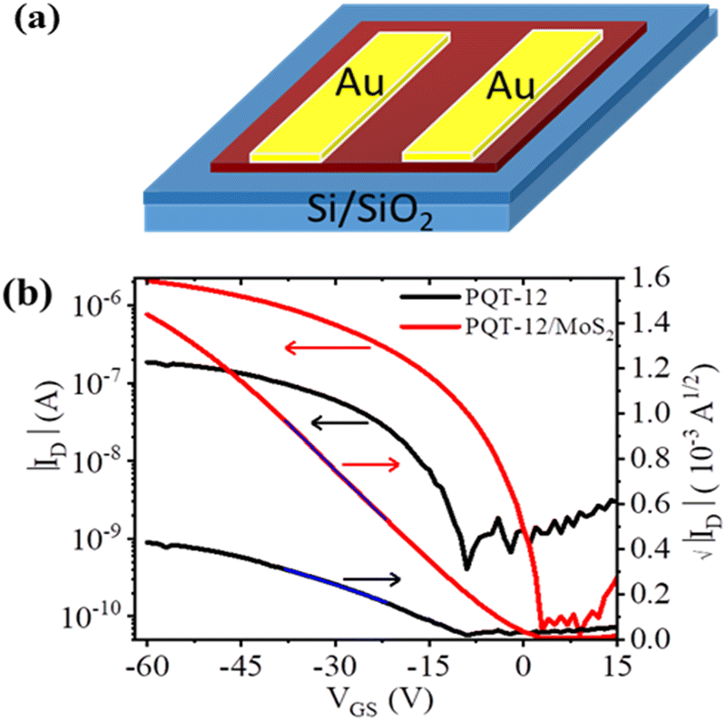 | ||
| Fig. 6 (a) Schematic representation of the fabricated OFET devices. (b) Transfer characteristics of pristine PQT-12 and PQT-12/MoS2 film-based OFETs. | ||
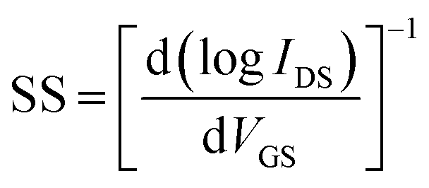
The subthreshold swing can also be related to the density of interfacial traps (Ninterface) and density of deep/shallow bulk traps (Nbulk) by the equation40,41
 | (4) |
This may be simplified as follows
 | (5) |
 is the thermal voltage and q is the unit charge. From eqn (3) the subthreshold swing is extracted as 5.93 V dec−1 for pristine and 3.21 V dec−1 for composite devices. The deep interfacial trap density was calculated to be 6.17 × 10¹² eV−1 cm−2 and 3.31 × 10¹² eV−1 cm−2 for the PQT-12 and PQT-12/MoS2 nanocomposite, respectively. The decrease in trap density explains the enhancement of charge transport in the nanocomposite. Also, a positive shift in the VTh from −9 V for pristine PQT-12 to 3 V for the PQT-12/MoS2 nanocomposite is observed. This might be associated with enhancement of molecular ordering in the polymeric chains after incorporation of MoS2 in PQT as evident by UV-vis spectroscopy.39 The on/off ratio for the PQT-12/MoS2 transistor is found to be 104, which is two orders of magnitude higher than that of the PQT-12 transistors (on/off ratio ∼ 102). Table 1 summarizes the performance of our fabricated OFETs.
| Device (transistors) | Mobility μ (cm2 V−1 s−1) | On/off ratio | Threshold voltage VTh (V) | Interfacial trap density (eV−1 cm−2) |
|---|---|---|---|---|
| PQT-12 | 0.4 × 10⁻³ | 102 | −9 | 6.17 × 10¹² |
| PQT-12/MoS2 | 3.6 × 10⁻³ | 104 | 3 | 3.31 × 10¹² |
Furthermore, the charge transport properties were investigated, particularly perpendicular to the film surface by sandwiched configuration Al/PQT-12/ITO and Al/PQT-12/MoS2/ITO. The unipolar conduction mechanism applies to Schottky diode-based structures as the current is controlled by majority charge carriers (in our case hole only). We chose ITO as the anode to create Ohmic contact with the HOMO level of active material and aluminum as the cathode to create a Schottky junction. The schematic representation of Schottky contact is shown in Fig. 7(a). After junction formation, the Gaussian-like distribution of the hole wavefunction at the HOMO level generally has a tail on the higher energy side which facilitates the thermionic emission of holes from the semiconductor to metal side to equilibrate the Fermi level. Non-linear behavior in the current density–voltage (J–V) characteristics reveals the formation of a Schottky barrier at the interface of the metal and semiconductor. Thus, the current density versus voltage plot can be elucidated by thermionic emission theory and Mott–Gurney law related to space charge limited current (SCLC). The J–V characteristics of the Al/PQT-12/ITO and Al/PQT-12/MoS2/ITO devices are shown in Fig. 7(b). The J–V relationship of the Schottky diode obeying the thermionic emission model is given by13,42
 | (6) |
 | (7) |
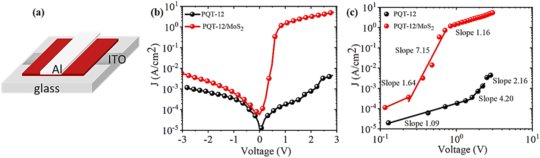 | ||
| Fig. 7 (a) Schematic representation of the fabricated SBD devices. (b) J–V characteristics of the ITO/PQT-12/Al and ITO/PQT-12-MoS2/Al devices. (c) logJ versus logV plot for Au/PQT-12/Al, and Au/PQT-12-MoS2/Al. | ||
A eff is the effective diode area, A* is the Richardson constant having value 1.2 A cm−2 K−2 and φB is the barrier height. In forward bias conditions, i.e. qVD/ηkT ≫ 1, eqn (7) modifies as:42
 | (8) |
The ideality factor value for all the devices is measured from the slope of the linear region of the semi logarithmic J–V plot according to eqn (8). The ideality factor was obtained as 19 and 5 for devices ITO/PQT-12/Al and ITO/PQT-12-MoS2/Al, respectively. The decrease in ideality factor for the nanocomposite-based device is attributed to better formation of the interface, which is related to the enhanced morphology, increase in crystallinity and decrease in trap charge density, which results in better charge transport concluded from the above sections. Furthermore, the reverse saturation current density J0 was obtained by extrapolating the linear portion of semi-log J–V to the J axis, which is found to be 1.84 μA and 22.27 μA for ITO/PQT-12/Al and ITO/PQT-12-MoS2/Al diodes, respectively. The reverse saturation current density is used to calculate interfacial barrier height for the charge carriers φB by using eqn (7), which is estimated as 0.64 eV and 0.55 eV for ITO/PQT-12/Al and ITO/PQT-12-MoS2/Al, respectively. This reduction of barrier height might be due to the formation of a charge transfer complex, which facilitates creation of delocalized states that enhance the charge transport pathway as explained in the above sections. The electronic parameter of our fabricated Schottky diodes is given Table 2.
| Device | Ideality factor (η) | Reverse saturation current density J0 (μA cm−2) | Barrier height φB (eV) | Rectification ratio |
|---|---|---|---|---|
| ITO/PQT-12/Al | 19 | 1.84 | 0.64 | 10 |
| ITO/PQT-12/MoS2/Al | 5 | 23.27 | 0.55 | 103 |
Non-linear behavior in the J–V characteristics reveals the existence of different conduction mechanisms in the devices. The J–V characteristic follows a universal power law of the form J ∝ Vm. The value of exponent m defines various conduction mechanisms from ohmic to space charge limited conduction (trap free and trap assisted). Therefore, the slope of the double logarithmic J–V plot defines the dominant conduction mechanism. Fig. 7(c) depicts the double logarithmic J–V plot in the forward bias region, which shows three distinct zones namely A, B and C, each with different slopes for both the devices. The first region, i.e., A shows a linear relation which means Ohmic conduction prevailed in this region. Ohmic conduction is majorly dominated as the applied voltage is low in this region, the barrier at the interface prevents charge carriers from being injected and current mostly comes from intrinsic carriers that are produced thermally. Next, region B shows the exponential relation of current density with voltage and is defined by trap assisted space charge limited conduction (TASCLC). The current density and voltage in this region are related with the following equation:43
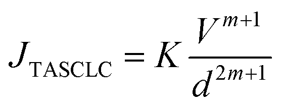 | (9) |
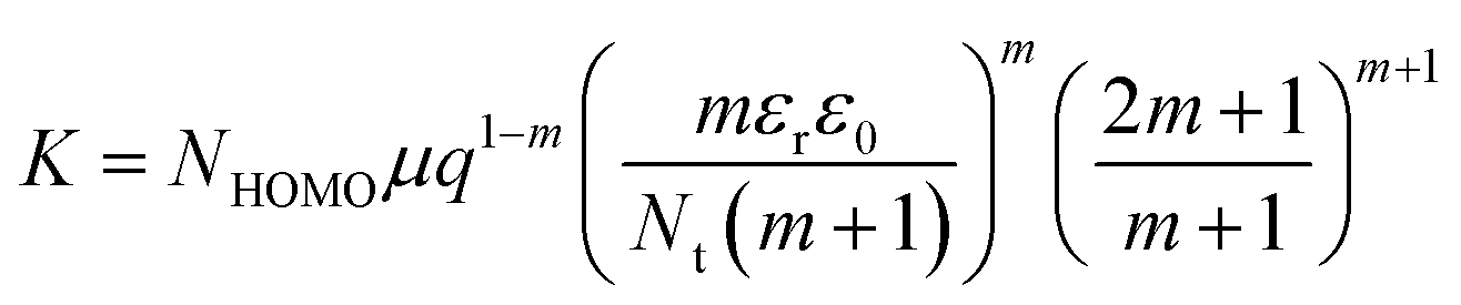 , and
, and 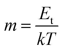 , the slope of region B, i.e., m quantifies the exponentially distributed trap states below the quasi Fermi level. NHOMO is the density of states in the highest occupied molecular orbital band, q is the electronic charge, μ is the intrinsic mobility, Nt and Et are the trap density and the characteristic trap distribution energy, respectively. The trap distribution energy has been evaluated from the slope of region B for both the devices and is found to be 108 meV and 185 meV, respectively for the PQT-12 and PQT-12-MoS2 devices. In region B, when the applied bias voltage is high enough to inject the carries from the ITO electrodes to the bulk of the semiconductor, the trap states in the semiconducting layer begin to fill and the current increases rapidly due to increased carrier density, resulting in the formation of TASCLC. On the further increase of the applied voltage, the devices enter into the trap free space charge limited conduction (TFSCLC) state where all the charge trapping centers present in the bandgap of the semiconducting layers are filled and the current is only due to space charge limited conduction; therefore this region is termed as trap free space charge limited conduction (TFSCLC). On comparing the plot for both the devices we can see that the transition from region A to region B and then to region C happens at lower bias voltage in the nanocomposite film than the pristine one. This can be explained by the lower barrier height and low trap density of the PQT-12/MoS2 based devices.
4. Conclusions
In conclusion, the integration of MoS2 nanosheets into PQT-12 polymer matrices has significantly enhanced the optical, structural, and electronic properties of the resulting nanocomposite thin films. The improved UV-Vis absorption spectra indicate better polymer chain ordering, while the photoluminescence quenching suggests stronger electronic interactions and nonradiative transitions. XRD analysis reveals increased crystallinity, denser molecular packing, and an extended coherence length, which is further supported by atomic force microscopy, showing a globular, interconnected nanofibrillar structure indicative of long polymer chains. These structural improvements contribute to more efficient charge transport pathways, as confirmed by superior electrical performance in organic field-effect transistors and Schottky diodes. The nanocomposite exhibits enhanced charge carrier mobility, reduced trap density, and an improved on/off and rectification ratio, demonstrating its potential for advanced electronic applications. Overall, these findings highlight the advantages of incorporating MoS2 nanosheets into conjugated polymer systems, leading to improved material properties and enhanced device performance.Data availability
Data supporting this study is included within the article.Conflicts of interest
There are no conflicts to declare.Acknowledgements
Mitu Chauhan and A. K. Singh acknowledge SERB (project SRG/2021/01326), India, for providing financial support during this work. A. K. Singh also acknowledges UGC-DAE-CSR, Indore (project CRS/2021-22/01/359) India, for support. V. C. acknowledges OCP project grant AS70 and ‘Chair Multiphysics’ led by Mohammed VI Polytechnic University and sponsored by OCP.References
- Y. Lee, B. Kang, S. Jung and J. Kwon, Npj Flex. Electron., 2024, 8, 41 CrossRef CAS.
- M. Erdoğan, A. R. Deniz and Z. Çaldıran, J. Photochem. Photobiol. Chem., 2023, 443, 114877 CrossRef.
- A. K. Singh and R. Prakash, RSC Adv., 2012, 2, 5277 RSC.
- M. Li, J. Zheng, X. Wang, R. Yu, Y. Wang, Y. Qiu, X. Cheng, G. Wang, G. Chen, K. Xie and J. Tang, Nat. Commun., 2022, 13, 4912 CrossRef CAS PubMed.
- V. Singh, A. K. Thakur, S. S. Pandey, W. Takashima and K. Kaneto, Org. Electron., 2008, 9, 790–796 CrossRef CAS.
- B. King and B. H. Lessard, J. Mater. Chem. C, 2024, 12, 5654–5683 RSC.
- W. B. Tarique and A. Uddin, Mater. Sci. Semicond. Process., 2023, 163, 107541 CrossRef CAS.
- T. Lv, W. Zhang, Y. Yang, J. Zhang, M. Yin, Z. Yin, K. Yong and Q. An, Small, 2023, 19, 2301071 CrossRef CAS PubMed.
- F. Yin, H. Niu, E. Kim, Y. K. Shin, Y. Li and N. Kim, InfoMat, 2023, 5, e12424 CrossRef.
- M. Hjort, A. H. Mousa, D. Bliman, M. A. Shameem, K. Hellman, A. S. Yadav, P. Ekström, F. Ek and R. Olsson, Nat. Commun., 2023, 14, 4453 CrossRef CAS PubMed.
- K. Gupta, N. Singh, R. S. Singh, U. P. Azad and A. K. Singh, J. Energy Storage, 2024, 103, 114348 CrossRef.
- V. Chaudhary, R. K. Pandey, R. Prakash, N. Kumar and A. K. Singh, Synth. Met., 2019, 258, 116221 Search PubMed.
- V. Chaudhary, R. K. Pandey, R. Prakash and A. K. Singh, J. Appl. Phys., 2017, 122, 225501 CrossRef.
- C. Kumar, G. Rawat, H. Kumar, Y. Kumar, R. Prakash and S. Jit, IEEE Trans. Nanotechnol., 2018, 17, 1111–1117 CAS.
- A. Kumar, D. K. Jarwal, A. K. Mishra, S. Ratan, C. Kumar, R. K. Upadhyay, B. Mukherjee and S. Jit, IEEE Photonics Technol. Lett., 2020, 32, 677–680 CAS.
- C. Kumar, G. Rawat, H. Kumar, Y. Kumar, R. Prakash and S. Jit, Org. Electron., 2017, 48, 53–60 CrossRef CAS.
- R. K. Pandey, A. K. Singh and R. Prakash, J. Phys. Chem. C, 2014, 118, 22943–22951 CrossRef CAS.
- R. K. Pandey, A. K. Singh, N. K. Singh, M. Rabelo, M. Ju, E.-C. Cho, R. Prakash and J. Yi, Appl. Surf. Sci., 2022, 593, 153413 CrossRef CAS.
- M. Pandey, S. S. Pandey, S. Nagamatsu, S. Hayase and W. Takashima, Thin Solid Films, 2016, 619, 125–130 CrossRef CAS.
- B. J. Akeredolu, I. Ahemen, A. N. Amah, A. D. Onojah, J. Shakya, H. N. Gayathri and A. Ghosh, Heliyon, 2024, 10, e24964 CrossRef CAS PubMed.
- A. H. Abdullah Ripain, N. A. A. Zulkifli, C. L. Tan, W. H. Abd Majid and R. Zakaria, Appl. Phys. Lett., 2023, 123, 061104 CrossRef CAS.
- M. Achqraoui, H. Jebari, N. Bekkioui and H. Ez-Zahraouy, Int. J. Hydrogen Energy, 2024, 51, 623–632 CrossRef CAS.
- V. Chaudhary, R. K. Pandey, P. K. Sahu, R. Prakash, N. Kumar and A. K. Singh, J. Phys. Chem. C, 2020, 124, 8101–8109 CrossRef CAS.
- T. Alamro and M. K. Ram, Electrochim. Acta, 2017, 235, 623–631 CrossRef CAS.
- J. Wang, Z. Wu, H. Yin, W. Li and Y. Jiang, RSC Adv., 2014, 4, 56926–56932 RSC.
- M. Makrygianni, A. Ainsebaa, M. Nagel, S. Sanaur, Y. S. Raptis, I. Zergioti and D. Tsamakis, Appl. Surf. Sci., 2016, 390, 823–830 CrossRef CAS.
- S. Jana, R. K. Pandey and R. Prakash, ACS Appl. Polym. Mater., 2022, 4, 4818–4828 CrossRef CAS.
- V. Chaudhary, R. K. Pandey, R. Prakash, N. Kumar and A. K. Singh, Nanotechnology, 2021, 32, 385201 CrossRef CAS PubMed.
- S. P. Tiwari, K. A. Knauer, A. Dindar and B. Kippelen, Org. Electron. Phys. Mater. Appl., 2012, 13, 18–22 CAS.
- S. Hayashi, Mater. Adv., 2020, 1, 632–638 RSC.
- R. K. Pandey, W. Takashima, S. Nagamatsu, A. Dauendorffer, K. Kaneto and R. Prakash, J Appl. Phys Search PubMed.
- W.-S. Syu, S.-C. Lin, S.-R. Tseng, C.-Y. Chen, C.-Y. Liu, Y.-C. Chao, H.-F. Meng and S.-F. Horng, Synth. Met., 2010, 160, 871–875 Search PubMed.
- S. Bhattacharyya and A. Patra, Bull. Mater. Sci., 2012, 35, 719–725 CrossRef CAS.
- G. L. Kabongo, P. S. Mbule, G. H. Mhlongo, B. M. Mothudi, K. T. Hillie and M. S. Dhlamini, Nanoscale Res. Lett., 2016, 11, 418 CrossRef PubMed.
- C. Kumar and S. Jit, IEEE Electron Device Lett., 2020, 41, 1556–1559 Search PubMed.
- M. Chauhan, R. S. Singh and A. K. Singh, Synth. Met., 2024, 306, 117624 CrossRef CAS.
- R. Ahmad, R. Srivastava, S. Yadav, S. Chand and S. Sapra, ACS Appl. Mater. Interfaces, 2017, 9, 34111–34121 CrossRef CAS PubMed.
- N. Nikhil, R. K. Pandey, P. K. Sahu, M. K. Singh and R. Prakash, J. Mater. Chem. C, 2018, 6, 9981–9989 RSC.
- R. K. Pandey, A. S. M. Tripathi, S. S. Pandey and R. Prakash, Carbon, 2019, 147, 252–261 CrossRef CAS.
- W. L. Kalb and B. Batlogg, Phys. Rev. B: Condens. Matter Mater. Phys., 2010, 81, 035327 CrossRef.
- Y. Kwon and B. Park, Thin Solid Films, 2016, 599, 145–150 CrossRef CAS.
- A. K. Singh, A. D. D. Dwivedi, P. Chakrabarti and R. Prakash, J. Appl. Phys., 2009, 105, 114506 CrossRef.
- S. Li, J. Chen and X. Zhou, Jpn. J. Appl. Phys., 2013, 52, 05DB11 CrossRef.
| This journal is © The Royal Society of Chemistry 2025 |