
 Open Access Article
 This Open Access Article is licensed under a Creative Commons Attribution-Non Commercial 3.0 Unported Licence
Pressure-induced multi-functional property analysis of lead-free tin based halide perovskites ASnCl3 (A = Ga, In, Tl) for advanced optoelectronic applications†
Md. Ratul
Hasan
 a,
Imtiaz Ahamed
Apon
*b,
Md. Mafidul
Islam
*a,
Asab Uzzaman
Azad
d,
Md.
Solayman
a and
Md. Salman
Haque
ac
a,
Imtiaz Ahamed
Apon
*b,
Md. Mafidul
Islam
*a,
Asab Uzzaman
Azad
d,
Md.
Solayman
a and
Md. Salman
Haque
ac
aDepartment of Materials Science and Engineering, Khulna University of Engineering & Technology (KUET), Khulna-9203, Bangladesh
bDepartment of Electrical and Electronic Engineering, Bangladesh Army University of Science and Technology (BAUST), Saidpur-5311, Bangladesh. E-mail: imti8509@gmail.com
cDepartment of Materials and Metallurgical Engineering, Bangladesh University of Engineering and Technology (BUET), Dhaka-1000, Bangladesh
dFaculty of Science, Engineering and Architecture, Laurentian University, Sudbury, Canada
First published on 6th February 2025
Abstract
This work examines the structural, electrical, and optical characteristics of lead-free tin-based halide perovskites, ASnCl3 (A = Ga, In, and Tl), as environmentally friendly substitutes for lead-based perovskites in solar applications. Hydrostatic pressures ranging from 0 to 8 GPa cause all three compounds – GaSnCl3, InSnCl3, and TlSnCl3 – to display a 3D-cubic perovskite structure. When pressure is applied, lattice parameters and unit cell volumes decrease as follows. For GaSnCl3, they decrease from 5.554 Å and 171.346 A3 to 5.161 Å and 137.515 A3; for InSnCl3, they are from 5.568 Å and 172.623 A3 to 5.178 Å and 138.891 A3; and for TlSnCl3, they are from 5.573 Å and 173.146 A3 to 5.184 Å and 139.352 A3. This suggests that the structure is stable under compression. These compound's formation enthalpies attest to their thermodynamic stability over the investigated pressure range. All three Sn-based compounds exhibit a direct bandgap at 0 GPa, and as pressure increases the band gap decreases, which suggests a tunable electronic structure. TlSnCl3 demonstrates a significant change from semiconductor to metallic behavior at higher pressures. The optical absorption spectra of the materials shift towards longer wavelengths (redshift) as pressure increases, enhancing the light absorption capabilities of these compounds. The compounds exhibit enhanced mechanical stability and ductility with increasing pressure, as indicated by their bulk, shear, and Young's modulus. Poisson's ratio values for these materials are in the range of 0.372 to 0.441 for GaSCl3, 0.355 to 0.418 for InSnCl3, and 0.349 to 0.413 for TlSnCl3, which highlights their ductile nature. GaSnCl3, InSnBr3, and TlSnCl3 exhibit diamagnetic behavior both under normal conditions and with increased pressure. Thermal conductivity and stability are enhanced with increased pressure, making these materials suitable for high-temperature applications. The ability to tune the properties of these compounds through pressure makes them promising candidates for next-generation optoelectronic devices, energy storage, and conversion systems.
Introduction
The first perovskite-based research began in the early 19th century with the mineral perovskite (calcium titanium oxide, CaTiO3) first being discovered in 1839 by German mineralogist Gustav Rose in the Ural Mountains of Russia.1 Scientists are presently dedicating substantial resources to discover materials that have practical applications, such as solar energy converters, memory devices, optical devices, sensors, and high-temperature sensors.2–4 First-principles calculations can elucidate the physical characteristics of a wide range of materials, and their findings are corroborated by practical investigations on these materials.5,6 Halogen-based cubic perovskites with the conventional formula ABX3 are attracting attention due to their remarkable characteristics, such as photodegradability, di-electricity, ferroelectricity, pyroelectricity, magnetism, and superconductivity.7–14 From a fundamental and technical perspective, these perovskites are becoming increasingly intriguing. The formula ABX3 represents a compound where X represents a halogen anion, while A and B represent monovalent and divalent cations, respectively.15 Almost all of the lead-based studies by different researchers such as Rehman et al.,16 Ghani et al.,17 Selmani et al.,18 Sidik et al.,19 Khan et al.20 illustrate that Pb-based cubic perovskites have a larger band gap ranging from 1.801 eV to 2.337 eV, 1.35 eV to 2.29 eV, 1.87 eV to 0.98 eV, 1.24 eV to 2.27 eV, and 0.87 to 1.89 eV, respectively.21,22 However, Sn-based perovskites exhibit a smaller band gap, which is crucial for absorbing more photons, generating a higher number of charge carriers, and enhancing efficiency in energy-conversion and light-emission devices. In contrast, lead-based perovskites can sometimes suffer from phase segregation and instability under light exposure.23–34 However, the incorporation of cations like Ga, In, and Tl promotes structural and chemical stability within the perovskite lattice. Furthermore, the ability of ASnCl3 (where, A = Ga, In, and Tl) to respond to pressure by tuning their structural, optical, and electronic properties makes these materials highly suitable for optoelectronic and energy-related applications. The choice of studying GaSnCl3, InSnCl3, and TlSnCl3 is motivated by the need for non-toxic, environmentally friendly alternatives, making them a superior choice compared to lead-based perovskites.Earlier research on doped Cs-based cubic halide perovskites was mainly focused on the investigation of their thermal and optical properties.35,36 Theoretical analysis of perovskite materials also reveals the potential effect of their use in optoelectronics and photocatalytic applications because of their intermediate band gap transition from an indirect band gap to direct band gap.37–42 Materials capable of mitigating the heating effects and reducing the efficiency of optical electronics can generate phonons via the indirect band gap.43,44 In addition, the physical properties of perovskite compounds can be modified through processes such as doping,45,46 chemical alteration,47 and the application of hydrostatic pressure.21,22,48–60 The latest study has shown that Sn-based cubic halide perovskites, such as LiXCl3 (X = Sn, Pb)17 and ZSnCl3 (Z = Na/K),61 have significant potential for a wide range of optoelectronic applications. However, the impact of varying hydrostatic pressure has great potential as a viable option for solar cell applications, such as NaGeX3.62 The existence of Pb poses significant risks to human health and the environment, making the need for lead-free cubic halide perovskites a high priority. Sn-based lead-free cubic halide perovskites, such as ASnX3 (A = K, Rb; X = Cl, Br, I),63 RbSnX3 (X = Cl, Br),64 KMCl3 (M = Ge, Sn),65 and CsSnCl3,54 have gained significant attention due to their environmentally friendly nature. These materials have been extensively studied under pressure-driven conditions. A thorough investigation was carried out using first-principles density functional theory (DFT) to analyze the impact of hydrostatic pressure on the electronic structure of CsSnX3 (X = I, Br, Cl) compounds.66 The objective of the study carried out by Imtiaz Ahamed Apon et al.67 was to investigate the mechanical, magnetic, elastic, electrical, and optical characteristics of the halide-based perovskites FrSnX3 (X = Cl, Br, and I) under hydrostatic pressures ranging from 0 to 6 GPa. In 2024, Hasan et al. undertook a study to achieve the greatest bandgaps,68 which were measured at 1.14, 0.8, and 0.645 eV, respectively. Insufficient research has been conducted on the effects of hydrostatic pressure on InSnCl3, GaSnCl3, and TlSnCl3, apart from the alkali materials. This also includes the results of the initial DFT calculations for various compounds, namely TlBX3 (B = Ge, Sn; X = Cl, Br, I),69 TlSnX3 (X = Cl, Br, or I),70 TlZX3 (Z = Ge, Sn, Be, Sr; X = Cl, Br, I),71 InSnX3 (X = Cl, Br, I),72 and InACl3 (A = Ge, Sn, Pb).20
The mystery from the deep ocean to outer space is still not fully uncovered, and the characteristics of the environment are also uncertain, particularly the hydrostatic pressure that intensifies with increasing ocean depth.73 In tin-based perovskites (ASnCl3, A = Ga, In, and Tl), the choice of A-site cations is crucial for stability and analyzing material properties.74 Ga, In, and Tl provide suitable ionic radii for structural integrity, particularly under pressure. Their electronic configurations of Ga (3d10 4s2 4p1), In (4d10 5s2 5p1), and Tl (5d10 6s2 6p1) introduce fine-tuning the bandgap, enhancing light absorption and charge carrier mobility for optoelectronic applications. These Ga, In, and Tl cations also improve environmental stability by resisting oxidation,75,76 whereas tin-based perovskites like CsSnCl3 are prone to oxidation, which degrades their performance.77 In-based perovskites show promising behavior in thermoelectrics, the Tl heavy atom effect aids spintronics,78 and finally Ga offers a balance of stability and performance in optoelectronic devices.
In this research, hydrostatic pressures are applied to lead-free tin-based halide perovskites (ASnCl3, where A = Ga, In, Tl). The results show that as pressure increases, the material's lattice parameters and unit cell volumes decrease, confirming their structural stability. This pressure application leads to a reduction in the band gap, allowing the tuning of the electronic structure, which is critical for optoelectronic applications. Additionally, optical absorption spectra shift towards longer wavelengths (redshift) with increasing pressure, enhancing the material's light absorption capabilities.
Computational method
This research is based on density functional theory (DFT) computations using the CASTEP packages,79 which also provides numerous and significant benefits for various optoelectronic application research. This research also utilizes the Vanderbilt-type ultrasoft pseudopotential80 along with the Perdew–Burke–Ernzerhof (PBE)81 program parameterized generalized gradient approximate (GGA) exchange–correlation functional for property analysis. The rSCAN meta-GGA and GGA-PBESol functionals were also used to compare the accuracy of the GGA-PBE functional in this study. These methods are utilized in the ab initio self-consistent field linear combination of atomic orbitals (SCF-LCAO) computer program CASTEP. The objective is to produce the geometrically optimized unit cell architecture of ASnCl3 (A = Ga, In, and Tl) perovskites. Limited-memory Broyden–Fletcher–Goldfarb–Shanno (LBFGS) was employed as the optimized algorithm by targeting energy convergence at 2.0 × 10⁻⁶ eV per atom displacement of 0.001 Å. The k-point mesh used has dimensions of 8 × 8 × 8. It allows for distinguishing between core states and valence levels. This distinction is facilitated by the plane-wave basis sets with a cut-off energy of 700 eV with a max iteration of 500. This strategy also uses 500 SCF cycles with a maximum force of 0.025 eV Å−1. The pseudopotentials used were OTFG with a Koelling–Hamon relativistic treatment. The electronic configurations for the calculation were Ga [3d10 4s2 4p1], Sn [4d10 5s2 5p2], and Cl [3s2 3p5] for GaSnCl3; In [4d10 5s2 5p1], Sn [4d10 5s2 5p2], and Cl [3s2 3p5] for InSnCl3; and Tl [4f14 5d10 6s2 6p1], Sn [4d10 5s2 5p2], and Cl [3s2 3p5] for TlSnCl3.Results and discussion
Structural properties
The optimized external stress with crystal structure and the intriguing physical properties of the perovskite materials under research are examined here in the hydrostatic pressure range of 0 to 8 GPa and the calculation was conducted on the space group Pm3m (no. 221). InSnCl3, GaSnCl3, and TlSnCl3 exhibit 3D-cubic crystal structures with the structural formula ABX3. The A atom occupies the 1a Wyckoff site at coordinates (0, 0, 0), positioned at the corners of the cube. The B atom, tin (Sn), is situated at the 1b Wyckoff site at (0.5, 0.5, and 0.5) which is located at the center within the body of the cube. The X atoms, which can be Cl occupy the 3c Wyckoff sites at (0, 0.5, 0.5), positioned at the face-centered locations of the cube (Fig. 1).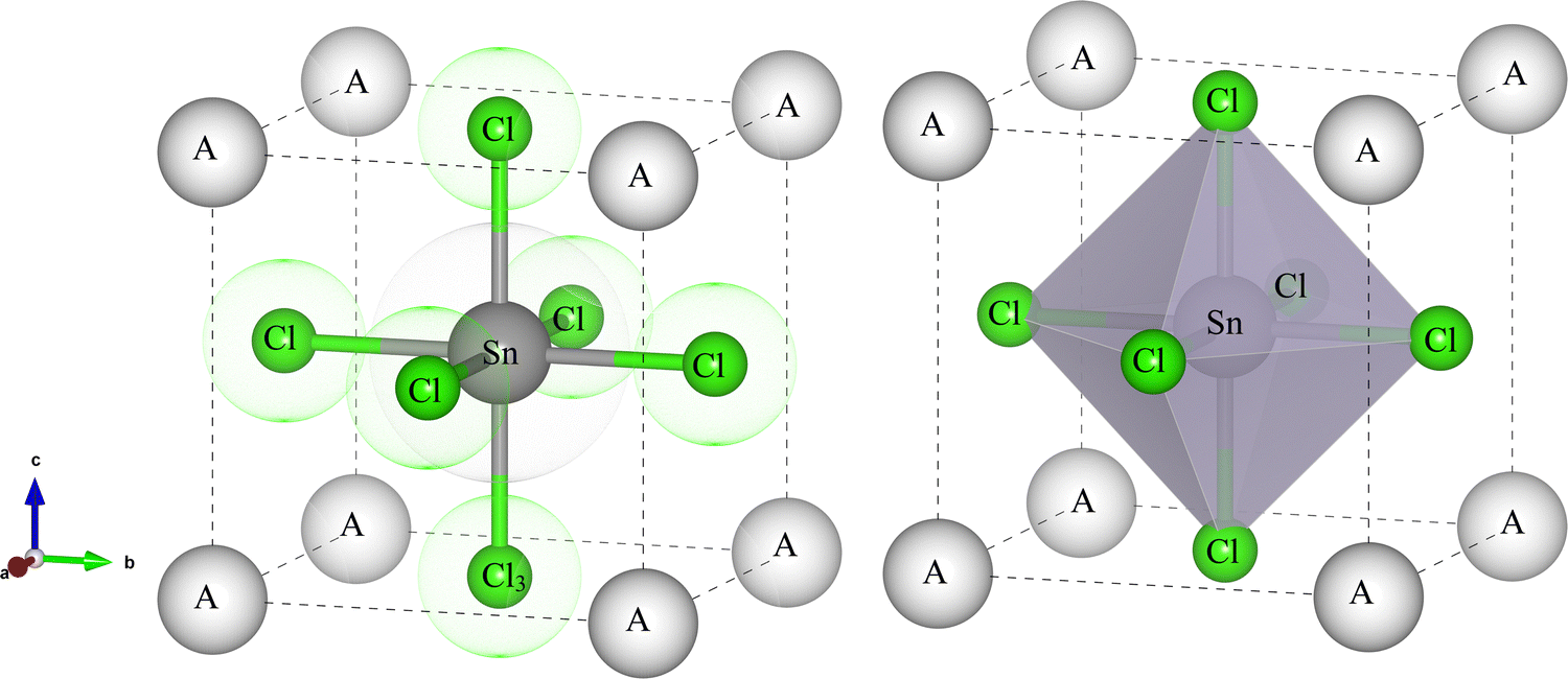 | ||
| Fig. 1 The crystal structure of ASnCl3 (A = Ga, In, and Tl). | ||
The analysis of the materials' structural properties provides a great comprehensive understanding of how pressure influences the physical and other similar properties of GaSnCl3, InSnCl3, and TlSnCl3. This understanding is very important for their potential use in advanced materials and optoelectronic devices. Table 1 illustrates the lattice parameters, unit cell volumes and the formation enthalpy of the compounds GaSnCl3, InSnCl3, and TlSnCl3.
| Compound | Calculated data | Pressure (GPa) | |||||
|---|---|---|---|---|---|---|---|
| 0 | 2 | 3 | 5 | 6 | 8 | ||
| GaSnCl3 | a (Å) | 5.554 | 5.419 | 5.365 | 5.271 | 5.232 | 5.161 |
| V (Å3) | 171.346 | 159.181 | 154.458 | 146.457 | 143.232 | 137.515 | |
| ΔEf (eV per atom) | −3.338 | −2.928 | −2.733 | −2.357 | −2.177 | −1.827 | |
| Band gap (eV) | 0.248 | 0 | 0 | 0 | 0 | 0 | |
| InSnCl3 | a (Å) | 5.568 | 5.434 | 5.378 | 5.287 | 5.250 | 5.178 |
| V (Å3) | 172.623 | 160.481 | 155.619 | 147.840 | 144.708 | 138.891 | |
| ΔEf (eV per atom) | −3.303 | −2.888 | −2.691 | −2.313 | −2.130 | −1.777 | |
| Band gap (eV) | 0.690 | 0.115 | 0 | 0 | 0 | 0 | |
| TlSnCl3 | a (Å) | 5.573 | 5.439 | 5.385 | 5.293 | 5.253 | 5.184 |
| V (Å3) | 173.146 | 160.909 | 156.189 | 148.303 | 144.989 | 139.352 | |
| ΔEf (eV per atom) | −3.425 | −3.010 | −2.812 | −2.432 | −2.249 | −1.894 | |
| Band gap (eV) | 0.878 | 0.300 | 0.044 | 0 | 0 | 0 | |
The compounds were subjected to hydrostatic pressures ranging from 0 to 8 GPa. The lattice parameter of the GaSnCl3 reduces from 5.554 Å at ambient pressure to 5.161 Å at 8 GPa. Similarly, the lattice parameters reduced from 5.568 Å to 5.178 Å, and from 5.573 Å to 5.184 Å for the compounds InSnBr3 and TlSnCl3 respectively. The crystal lattice is compressed under high pressure, and this results in a compact arrangement of atoms.82 The substitution of the ‘A’ atom position by different sizes eventually affects the lattice constants and volumes by demonstrating the octahedral factor effect due to the periodic pattern of the size of the atoms. The structural properties are influenced by the size of the A site ion; compounds with larger A site ions exhibit higher lattice constants and atomic volumes.67
The volume of the unit cell also decreases after applying hydrostatic pressure up to 8 GPa. The volume of GaSnCl3 decreases from 171.346 Å3 to 137.515 Å3, InSnBr3 from 172.623 Å3 to 138.891 Å3 and TlSnCl3 from 173.146 Å3 to 139.352 Å3 at 8 GPa applied pressure. The relationship between energy and volume is depicted using the Birch–Murnaghan equation of state, demonstrating that energy decreases with decreasing unit cell volume until reaching a minimum at the ground-state energy. Murnaghan's equation of state is as follows:
 | (1) |
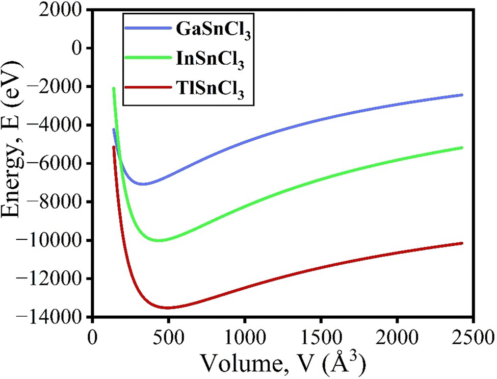 | ||
| Fig. 2 The total energy as a function of unit cell volume of the cubic ASnCl3 (A = Ga, In, Tl). | ||
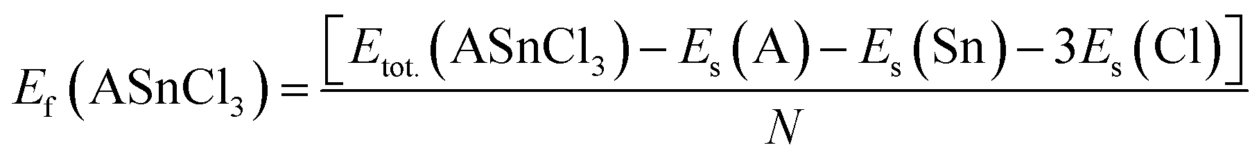
The formation enthalpy of these compounds was calculated using the formula:
 | (2) |
The tolerance factor (t) of these compounds is calculated by using the formula stated below:
 | (3) |
| Ref. | Compound | Band gap (eV) | Lattice constants (Å) | Volume (Å3) | Function |
|---|---|---|---|---|---|
| 61 | NaSnCl3 | 1.36 | 5.598 | 175.447 | HSE06 |
| KSnCl3 | 1.47![[thin space (1/6-em)]](https://www.rsc.org/images/entities/char_2009.gif) |
5.631 | 178.574 | ||
| NaSnCl3 | 0.71 | 5.598 | 175.447 | PBE | |
| KSnCl3 | 0.78 | 5.631 | 178.574 | ||
| NaSnCl3 | 1.04 | 5.598 | 175.447 | RPBE | |
| KSnCl3 | 1.10 | 5.631 | 178.574 | ||
| 65 | KSnCl3 | 0.91 | 5.58 | 173.80 | GGA-PBE |
| 84 | CsSnCl3 | 0.55 | 5.510 | — | PBESol |
| 1.4 | 5.750 | — | rPBE | ||
| 2.91 | 5.563 | — | GW | ||
| 85 | CsSnCl3 | 2.8 | 5.620 | — | Experimental |
| CsSnBr3 | 2.0 | 5.870 | — | ||
| CsSnI3 | 1.3 to 1.4 | 6.230 | — | ||
| 86 | CsSnCl3 | 3.0 | 5.560 | — | Experimental |
| CsSnBr3 | 1.7 to 2.1 eV | 5.804 | — | ||
| 54 | CsSnCl3 | 0.943 | 5.61 | 176.56 | GGA-PBE |
| 87 | RbSnCl3 | 0.88 | 5.596 | — | GGA-PBE |
| RbSnBr3 | 0.61 | 5.891 | — | ||
| KSnCl3 | 0.89 | 5.596 | — | ||
| KSnBr3 | 0.57 | 5.873 | — | ||
| 88 | RbSnCl3 | 0.878 | 5.581 | — | GGA-PBE |
| RbSnBr3 | 0.556 | 5.853 | — | ||
| RbSnI3 | 0.383 | 6.249 | — | ||
| 89 | FrSnCl3 | 1.050 | 5.64 | — | GGA-PBE |
| FrSnBr3 | 0.670 | 5.90 | — | ||
| FrSnI3 | 0.420 | 6.27 | — | ||
| 67 | FrSnCl3 | 1.046 | 5.645 | 179.855 | GGA-PBE |
| FrSnBr3 | 0.675 | 5.906 | 206.038 | ||
| FrSnI3 | 0.485 | 6.299 | 249.927 | ||
| 20 | TlGeCl3 | 0.910 | 5.262 | 145.658 | GGA-PBE |
| TlGeBr3 | 0.570 | 5.521 | 168.246 | ||
| TlGeI3 | 0.420 | 5.897 | 205.024 | ||
| TlSnCl3 | 0.880 | 5.573 | 173.073 | ||
| TlSnBr3 | 0.520 | 5.826 | 197.788 | ||
| TlSnI3 | 0.300 | 6.203 | 238.711 | ||
| This work | GaSnCl3 | 0.248 | 5.554 | 171.346 | GGA-PBE |
| InSnCl3 | 0.690 | 5.568 | 172.623 | ||
| TlSnCl3 | 0.878 | 5.573 | 173.146 | ||
| GaSnCl3 | 0.000 | 5.435 | 160.564 | GGA-PBESol | |
| InSnCl3 | 0.078 | 5.443 | 161.263 | ||
| TlSnCl3 | 0.281 | 5.451 | 161.984 | ||
| GaSnCl3 | 0.000 | 5.486 | 165.120 | m-GGA-RSCAN | |
| InSnCl3 | 0.455 | 5.501 | 166.512 | ||
| TlSnCl3 | 0.647 | 5.499 | 166.292 |
GaSnCl3 and InSnCl3 exhibit similar or more compact parameters of lattice constants and unit cell volume compared to other compounds. The lattice constants and volumes of InSnCl3 are smaller than those of the experimentally synthesized compounds CsSnCl3 and CsSnBr3.85 This illustrates that the compounds ASnCl3 (A = Ga, In and Tl) are more stable and less prone to expansion under hydrostatic applied pressure conditions. The compound TlSnCl3 exhibits a band gap of 0.880 eV69 which is closer to this study with a value of 0.878 eV. Our results provide competitive values that align well with existing data with more precise measurements that can be beneficial for practical applications.
Electronic properties
Investigating the electronic properties is crucial for understanding the overall behavior of InSnCl3, GaSnCl3, and TlSnCl3. The electronic band structures and density of states (DOS) were analyzed using the PBE functional within the GGA approximation, emphasizing the high symmetrical directions of the Brillouin zone. The band gap values and DOS for these compounds under hydrostatic pressure ranging from 0 to 8 GPa are presented in Fig. 3 and 4, respectively. The range for the valence band to conduction band is −30 eV to +30 eV and 0 eV represents the Fermi level (EF).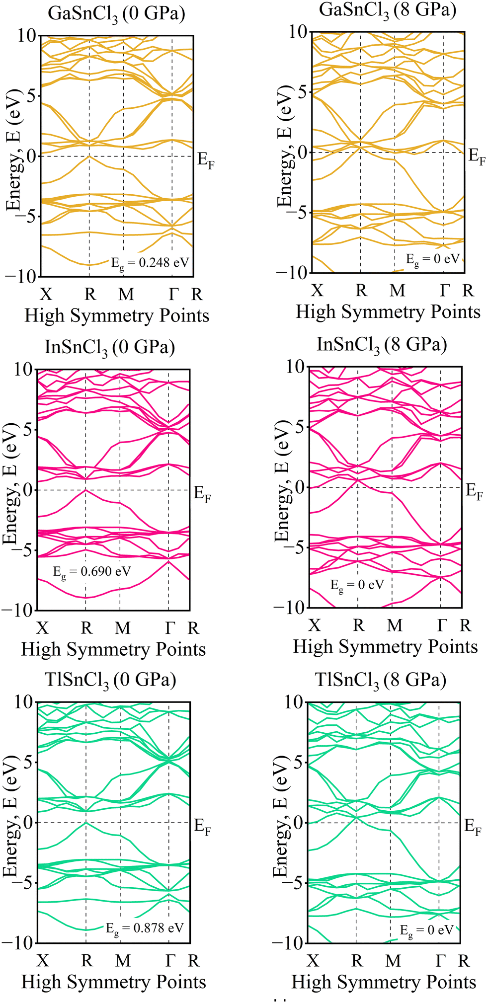 | ||
| Fig. 3 Band structure of ASnCl3 (A = Ga, In, and Tl) under pressure. | ||
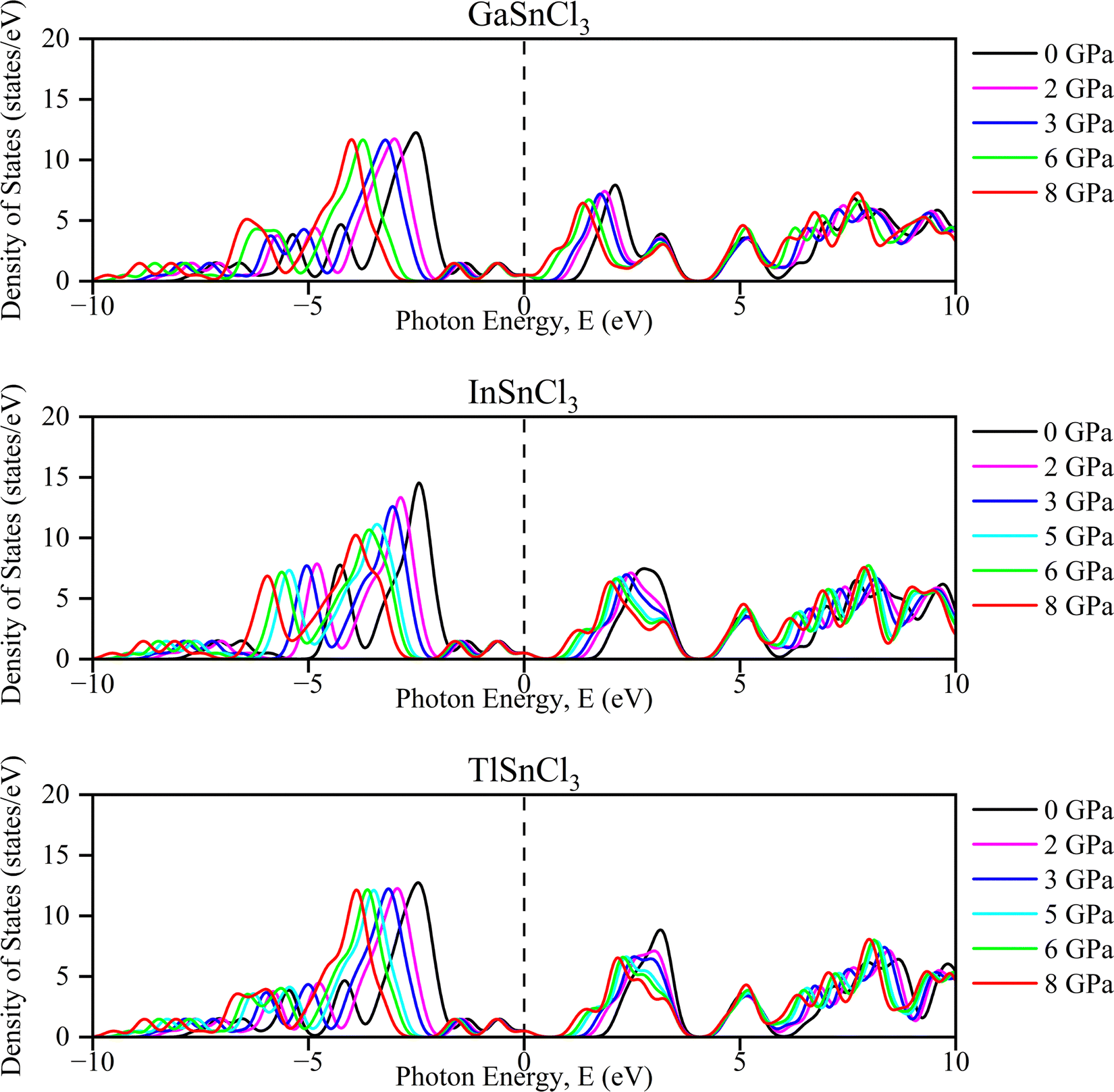 | ||
| Fig. 4 Total density of states (TDOS) of ASnCl3 (A = Ga, In, and Tl) under pressure. | ||
The band gap represents the energy difference between the conduction and valence bands. The observed materials exhibit a direct bandgap because of the high symmetry of the crystal structure. As pressure increases, the band gap decreases for all InSnCl3, GaSnCl3, and TlSnCl3 compounds. Larger atoms at the A sites result in smaller band gaps. Under high pressures up to 8 GPa the compounds become conductive. Fig. 3 shows that GaSnI3 and TlSnI3 exhibit conductive properties at 2 GPa, and InSnCl3 requires 5 GPa to achieve similar conductivity.
At 0 GPa, the DOS of GaSnCl3 around the Fermi level exhibits a small bandgap (no states around 0 eV), indicating a semiconducting nature at ambient pressure. The states below the Fermi level are dense from −10 eV to around −3 eV, which indicates the valence band. There is a clear separation of the conduction band, which starts slightly above 1 eV. With increasing pressure of GaSnCl3 from 2 GPa to 8 GPa, the bandgap narrows as indicated by the states moving closer to the Fermi level, particularly at 2 GPa and 3 GPa. At higher pressures (6 GPa and 8 GPa), the gap diminishes significantly, and states near the Fermi level begin to appear, indicating a transition towards a more metallic character. The increased states around 0 eV suggest that GaSnCl3 may become conductive at these higher pressures.
At 0 GPa, InSnCl3 also exhibits a noticeable bandgap around the Fermi level, although smaller than GaSnCl3, suggesting it has semiconducting properties at ambient pressure. The valence band states are concentrated between −10 eV to about −2 eV, with a well-defined gap separating the conduction band. With increasing pressure of InSnCl3, the bandgap narrows progressively. By 3 GPa and beyond, states around the Fermi level begin to appear, particularly at 6 GPa and 8 GPa, where the DOS plot shows significant electronic states near and at the Fermi level. This behavior implies a pressure-induced semiconducting-to-metallic transition, like GaSnCl3, but the transition occurs more gradually in InSnCl3.
At 0 GPa, TlSnCl3 demonstrates a bandgap around the Fermi level, showing its semiconducting nature. The valence band is more widespread, extending from −10 eV to approximately −1.5 eV. The conduction band starts above the gap, at about 1.5 eV. As pressure increases, the bandgap narrows similarly to the other two compounds. However, the transition seems more rapid in TlSnCl3, with states appearing near the Fermi level as early as 3 GPa. At 5 GPa and 6 GPa, the DOS around the Fermi level increases significantly, suggesting that TlSnCl3 undergoes a faster transition to a metallic state compared to GaSnCl3 and InSnCl3. At 8 GPa, the Fermi level intersects several states, indicating strong metallic behavior.
The partial density of states (PDOS) of InSnCl3, GaSnCl3, and TlSnCl3 at 0 to 8 GPa are illustrated in Fig. 5 which range from −16 eV to +16 eV. The significant peaks are observed below the Fermi level between −5 eV and 0 eV where the maximum peak is observed by the s-orbital. In the 5 eV energy range, the p-orbital and d-orbital show significant contributions. Above the Fermi level, fewer states are available, which can be observed from the smaller peaks primarily between 0 eV and 5 eV, which are typical of non-metallic or semiconductor materials states. The contribution of f-orbitals is quite low for visualization. These observations demonstrate that the energies below the Fermi level correspond to bonding states, while there is the presence of flat PDOS. This detailed orbital analysis helps in understanding the electronic properties and potential semiconductor and non-metallic material-based applications.
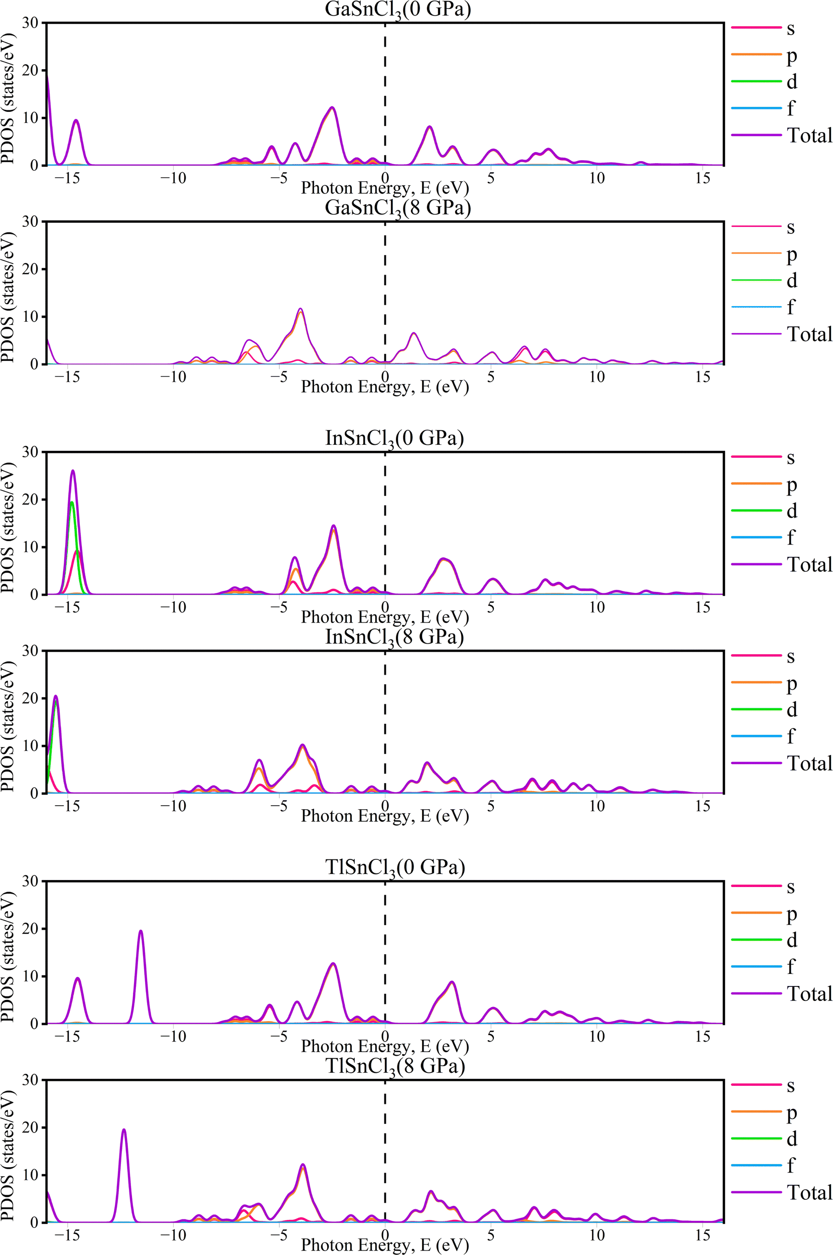 | ||
| Fig. 5 The partial density of states (PDOS) of ASnCl3 (A = Ga, In, and Tl) under pressure. | ||
Charge density
The charge density for ASnCl3 (A = Ga, In, and Tl) shows irregular charge density lines, which indicates the bonding between atoms. The effect of hydrostatic pressure up to 8 GPa on charge distribution was investigated for the compounds GaSnCl3, InSnCl3 and TlSnCl3. Fig. 6 shows the change in the spherical charge density lines and elliptical lines around the atoms Ga, In and Tl with respect to Cl and Sn atoms along the (100) plane and (200) plane respectively. The electron density is shown with a scale on the right side where blue indicates lower electron density and red indicates higher electron density.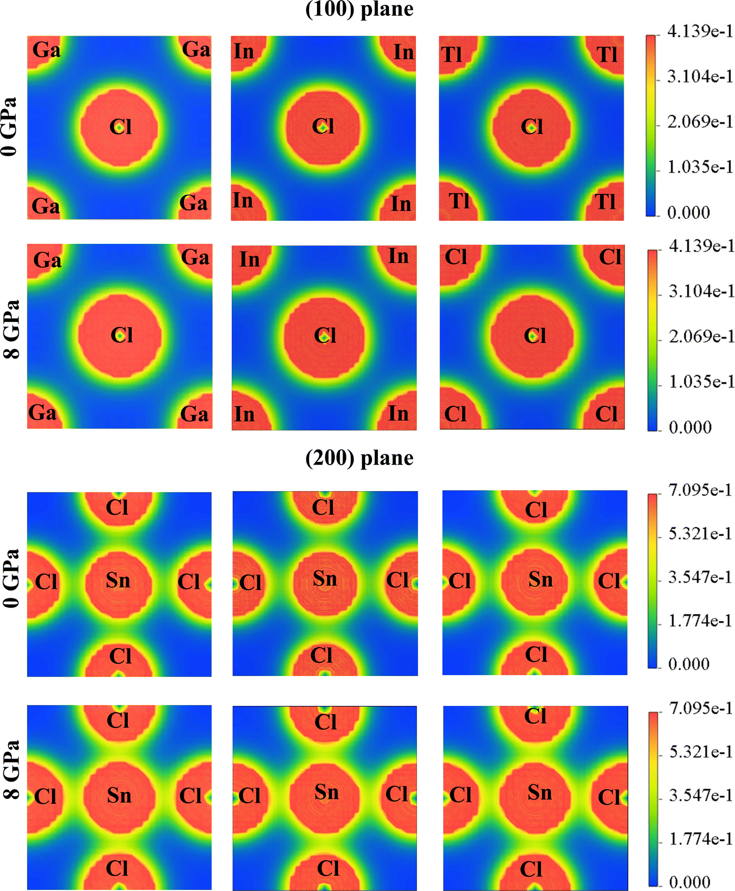 | ||
| Fig. 6 Charge density of ASnCl3 (A = Ga, In, and Tl) for pressures of 0 GPa and 8 GPa. | ||
The compounds ASnCl3 (A = Ga, In, and Tl) exhibit a covalent nature between “A” site atoms and the Cl atom which signifies the hardness nature of the compounds. The local field surrounding the A (Ga, In and Tl) atoms and Cl atoms represents the hybridization among the atomic states. The atoms with the highest electronegativity charges are attracted by most surrounding charges. The stronger covalent bond is observed at Sn–Cl bonding and A–Cl bonding depicts ionic bonds which are illustrated in Fig. 6. The surrounding area of the atoms also demonstrates that the covalent bonds between Sn–Cl are weaker compared to the ionic bonds between A–Cl (A = Ga, In, and Tl). After increasing pressure up to 8 GPa, the bonding between Ga/In/Tl and Cl atoms grows within more surrounding areas and the charge shows more elliptical contours around Sn–Cl atoms in the (200) plane.
The chemical bonding characteristics of RbSnX3 (X = Cl, Br) compounds from analyzing charge density mapping were investigated by Rashid et al. (2022).88 This article shows that the bonding between Rb and Cl/Br atoms belongs to strong ionic bonding compared to the covalent bonding between Sn and Cl/Br atoms at 0 GPa. On increasing pressure up to 10 GPa, the study revealed that the overlapping of charge density along the (100) plane and (200) plane increased compared to the 0 GPa mapping. This analysis reveals the electronic bond nature between the atoms in a compound and the impact of different atoms on the electronic properties and charge density mapping.
Optical properties
The optical properties of the ASnCl3 (A = Ga, In, and Tl) compounds provide a deep understanding of the electronic structure and density of states. The optical properties of materials such as conductivity, dielectric function, absorption, refractive index, and loss function also help in investigating material behaviors and reveal the interactions with the electromagnetic radiation, and are included in this section. | ||
| Fig. 7 Calculated pressure-induced spectra of absorption (α) for ASnCl3 (A = Ga, In, and Tl). | ||
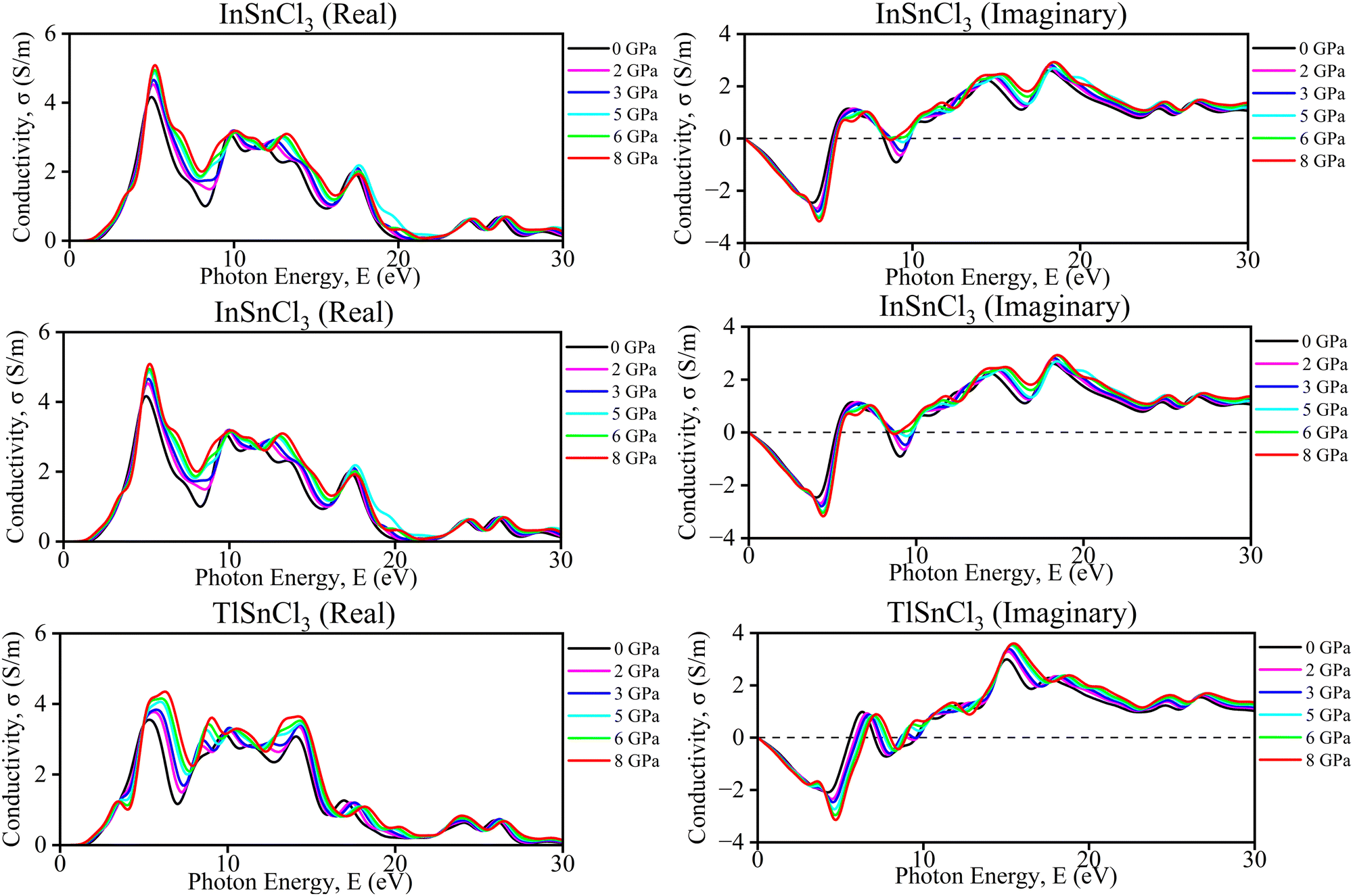 | ||
| Fig. 8 Calculated pressure-induced imaginary and real spectra of optical conductivity (σ) for ASnCl3 (A = Ga, In, and Tl). | ||
The graphs provide the imaginary and real components of the conductivity (σ) for InSnCl3 as a function of photon energy (E) in electron volts (eV) under different hydrostatic pressures ranging from 0, 2, 3, 5, 6, and 8 GPa. The observation from the imaginary conductivity graph shows oscillatory behavior with both positive and negative values which also indicates the energy storage and dispersion characteristics for increasing amplitude in the higher pressure's oscillation. On the other hand, the real conductivity graph represents generally positive values with distinct peaks at specific photon energies revealing an actual conducting behavior and trend of increasing magnitude with higher pressure. Each graph reveals that increasing pressures can affect the materials' conductivity, where higher pressures enhance both reactive and resistive properties of InSnCl3 by reflecting a complex interplay between the materials’ increased pressure and photon energies in determining the materials’ electrical properties.
For TlSnCl3, the real and imaginary components of the conductivity (σ) as a function of photon energy (E) are shown in Fig. 8. The real part of conductivity increased with increasing pressure up to 8 GPa. The highest peak of the real part of conductivity is observed in the ultraviolet range of this curve. Increasing pressure shifts both the real and imaginary parts, but the overall patterns remain consistent. The real conductivity values are generally higher than the imaginary ones, indicating a more significant energy dissipation component in the material's response. Both graphs together demonstrate how TlSnCl3 conductivity, in terms of energy loss (real part) and stored energy (imaginary part), varies with photon energy and applied pressure.
| ε(ω) = ε1(ω) + iε2(ω) | (4) |
 | (5) |
 | (6) |
We analyzed optical characteristics such as absorption coefficient, calculated from ε1(ω) and ε2(ω). ASnCl3 (A = Ga, In, and Tl) molecules are isotropic and homogenous, according to our research.
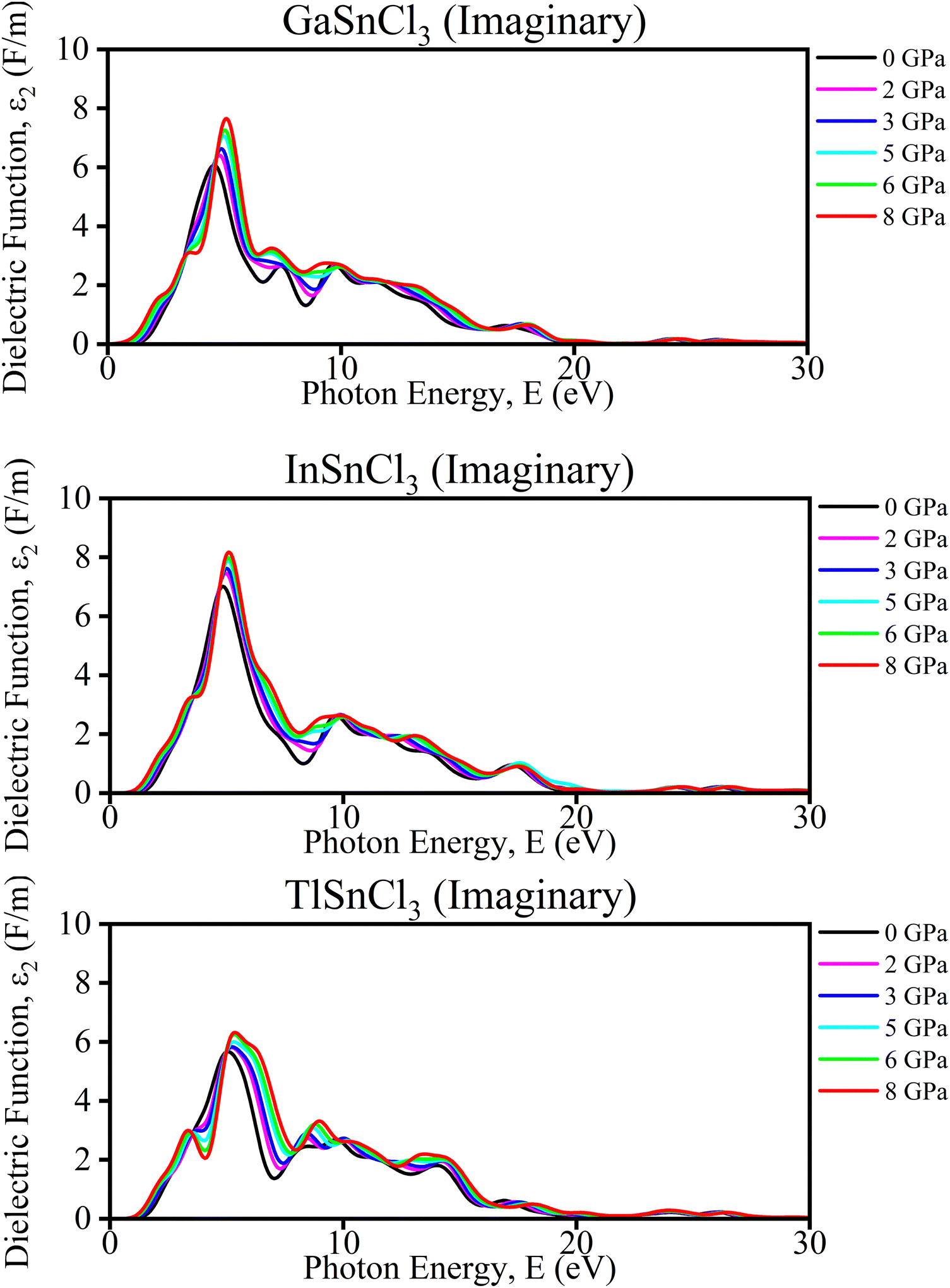
Imaginary part of the dielectric function. The analysis of TlSnCl3, GaSnCl3, and InSnCl3 under pressures from 0 to 8 GPa reveals several significant changes and benefits. As pressure increases, the main peak intensity of the dielectric function generally rises for all compounds, indicating enhanced optical absorption and dielectric response. Peaks also broaden slightly, suggesting a wider range of electronic transitions, and shift towards higher energies, reflecting changes in the electronic band structure. Higher pressures smooth out finer spectral features, particularly noticeable in the 8–15 eV range, while the dielectric function increases at lower energies (0–5 eV), potentially indicating improved conductivity or polarizability in Fig. 9.
 | ||
| Fig. 9 Calculated pressure induced imaginary spectra of dielectric function (ε) for ASnCl3 (A = Ga, In, and Tl). | ||
These pressure-induced changes offer several benefits. The ability to tune the optical and electronic properties through pressure adjustments provides valuable control over material characteristics. Increased peak intensities could enhance light absorption, which is beneficial for photovoltaic applications. The shift in peaks suggests that pressure can be used for bandgap engineering, crucial for semiconductor applications. The improved low-energy response may lead to better electrical conductivity at higher pressures. Overall, understanding these pressure effects aids in designing materials with specific optical and electronic properties for a variety of applications.
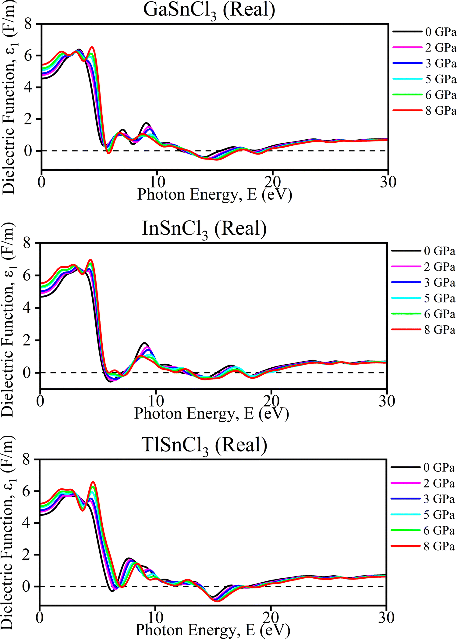
Real part of the dielectric function. The graphs (Fig. 10) illustrate the real part of the dielectric function (ε1) and conductivity (σ) as a function of photon energy for InSnCl3, TlSnCl3, and GaSnCl3 under varying pressures from 0 GPa to 8 GPa. For the dielectric function (ε1), each material displays a prominent peak around 4–6 eV, which gradually decreases as photon energy increases. As pressure rises, these peak positions shift slightly, and the overall value of ε1 diminishes, particularly around the initial peak. This effect is more noticeable in TlSnCl3, where the ε1 values decrease significantly with pressure compared to InSnCl3 and GaSnCl3. Regarding conductivity (σ), multiple peaks appear between 0 eV and 30 eV, representing different optical transitions in Fig. 10. With increasing pressure, these peak positions also shift slightly, and their magnitudes vary, although not as drastically as in the dielectric function.
 | ||
| Fig. 10 Calculated pressure induced real spectra of dielectric function (ε) for ASnCl3 (A = Ga, In, and Tl). | ||
These pressure-induced changes offer several benefits. The ability to tune the optical properties through pressure adjustments is advantageous for applications like photo detectors and solar cells. Understanding how pressure affects these properties enhances insights into material stability under different conditions, essential for high-pressure environment applications. Furthermore, the shift in peaks suggests potential for engineering specific electronic band structures, making these materials suitable for various electronic and photonic applications, depending on the desired optical response. Overall, the pressure dependence of the dielectric function and conductivity highlights the potential for precise control of these materials' optical properties, enabling their use in advanced technological applications.
Such a negative dielectric constant indicates the presence of metallic or plasmonic behavior, which can significantly affect the material's optoelectronic properties, making it suitable for applications that leverage these unique characteristics.69
Islam and Hossain et al. in 2020 observed that increasing pressure on CsSnCl3 perovskites leads to a rise in the static peak of dielectric constant which indicates a reduction in charge carrier recombination rate and enhanced efficiency of optoelectronic devices. The imaginary part of the dielectric function increases significantly with pressure that shifts to lower energy regions, suggesting an increase in absorption and transparency in high energy regions above 26 eV.38
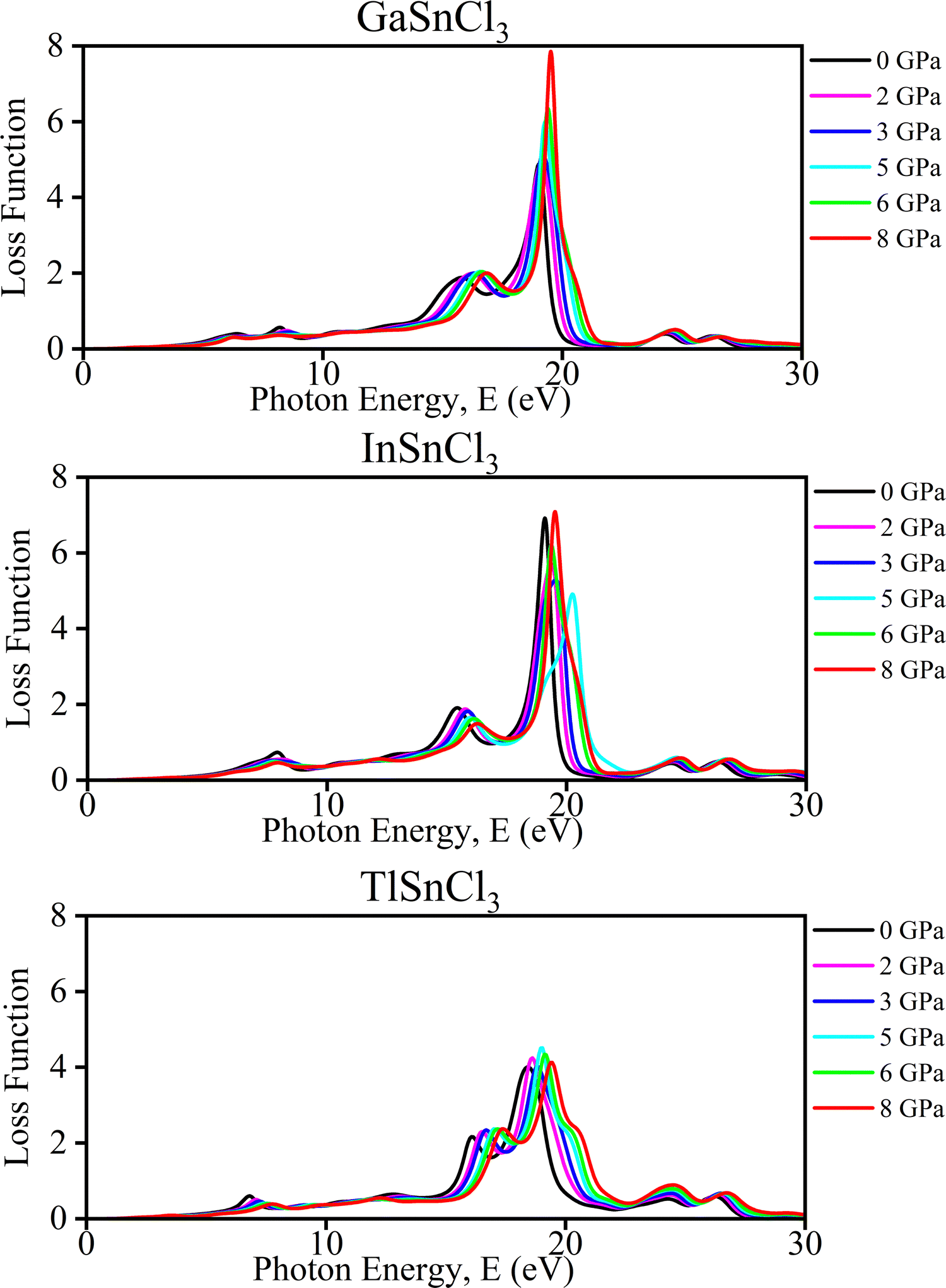 | ||
| Fig. 11 Calculated pressure-induced spectra of loss function of ASnCl3 (A = Ga, In, and Tl). | ||
These changes offer several benefits. The ability to tune the electronic and optical properties through pressure makes these materials suitable for applications requiring specific photon energy responses, such as in optoelectronics or sensor technologies. Understanding how these materials behave under pressure provides valuable insight into developing new materials with desirable properties for high-pressure environments.
 | ||
| Fig. 12 Calculated pressure induced spectra of the refractive index (n1) of ASnCl3 (A = Ga, In, and Tl). | ||
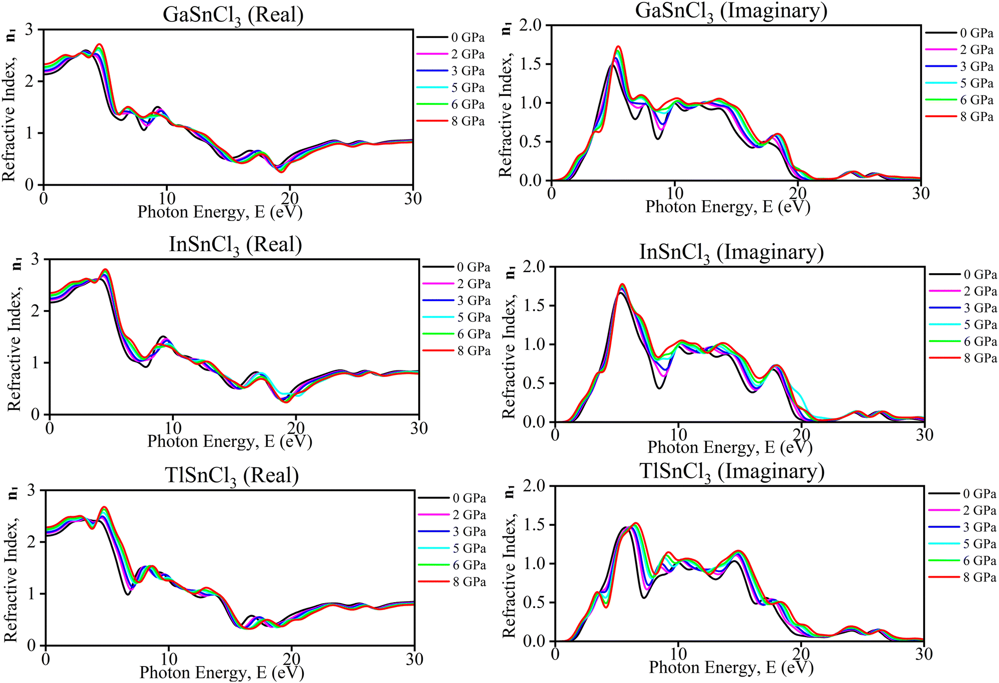
These observations offer several benefits. Understanding the changes in refractive index with pressure aids in designing materials for specific optical applications, such as pressure sensors and adaptive optical devices. The ability to tune the optical properties by applying pressure allows for dynamic control over material behavior, making these materials suitable for devices requiring adjustable optical properties. Insights from these graphs can inform the development of optoelectronic devices, like lasers and photodetectors, which demand precise control over light–matter interactions under varying environmental conditions. Additionally, examining the impact of pressure on these materials provides information about their structural stability, essential for long-term use in high-pressure environments. Overall, these graphs offer valuable data for optimizing materials for advanced optical and electronic systems. Mitro et al. in 2022 highlighted that increasing pressure on RbGeX3 perovskites (X = Cl, Br) results in a higher static refractive index, indicating greater light absorption potential. This suggests enhanced suitability for optoelectronic and photovoltaic device applications, generating considerable interest among researchers.90 Applying pressure makes certain materials better at absorbing photons in a specific energy range. Photo detectors, solar cells, and optical sensors need this property to absorb light.
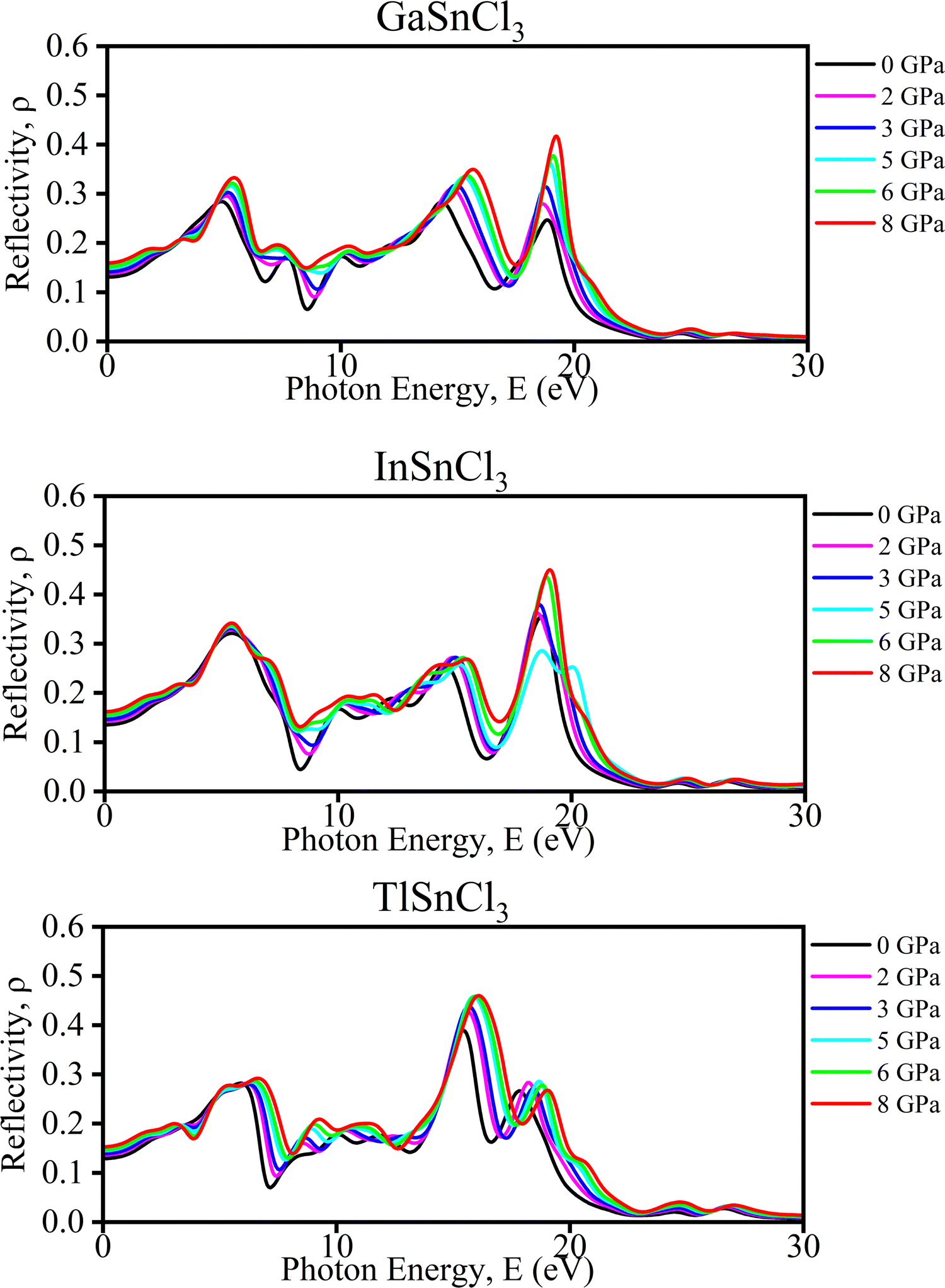 | ||
| Fig. 13 Calculated pressure induced spectra of the reflectivity (ρ) of ASnCl3 (A = Ga, In, and Tl). | ||
Haq et al. in 2021 illustrated that increasing pressure on KCaCl3 perovskites results in a rise in reflectivity in the low-energy region which decreases photovoltaic efficiency. While in the high-energy zone, the material's reflectivity increases suggesting better results for solar heating reduction.91 Although it stays in the infrared region and grows somewhat for all compounds, the range of the maximum peak is slightly affected by induced pressure. Due to the low reflectivity values in the low-energy range, ASnCl3 shows promising candidate for solar cell application, even under pressure. Additionally, these compounds are recommended for use as covering materials to reduce solar heating, owing to their higher reflectivity values in the high-energy range.92
Mechanical properties
Table 3 presents the elastic stiffness constants matrix Cij for the compounds GaSnCl3, InSnBr3, and TlSnCl3 calculated under different pressures (0, 2, 3, 5, 6, and 8 GPa). These constants, C11, C12, and C44, characterize the compounds' mechanical properties and how they change with pressure.| Ref. | Compound | Elastic constants | Pressure (GPa) | |||||
|---|---|---|---|---|---|---|---|---|
| 0 | 2 | 3 | 5 | 6 | 8 | |||
| This work | GaSnCl3 | C 11 | 51.251 | 69.263 | 77.823 | 95.920 | 103.910 | 119.945 |
| C 12 | 8.441 | 11.189 | 12.416 | 15.035 | 16.196 | 18.849 | ||
| C 44 | 1.882 | 0.351 | −0.303 | −1.371 | −1.960 | −3.180 | ||
| C 12–C44 | 6.559 | 10.838 | 12.719 | 16.406 | 18.156 | 22.029 | ||
| InSnCl3 | C 11 | 51.962 | 70.081 | 79.289 | 96.167 | 104.146 | 120.172 | |
| C 12 | 9.345 | 11.942 | 13.534 | 16.243 | 17.733 | 20.372 | ||
| C 44 | 3.103 | 2.240 | 1.780 | 0.850 | 0.397 | −0.599 | ||
| C 12–C44 | 6.242 | 9.702 | 11.754 | 15.393 | 17.336 | 20.971 | ||
| TlSnCl3 | C 11 | 51.204 | 69.761 | 78.687 | 95.862 | 104.107 | 119.799 | |
| C 12 | 9.017 | 12.137 | 13.660 | 16.552 | 17.976 | 20.832 | ||
| C 44 | 3.308 | 2.420 | 2.054 | 1.254 | 0.832 | −0.015 | ||
| C 12–C44 | 5.763 | 9.717 | 11.606 | 15.298 | 17.144 | 20.847 | ||
| 70 | TlSnCl3 | C 11 | 51.52 | — | — | — | — | — |
| C 12 | 8.81 | — | — | — | — | — | ||
| C 44 | 3.38 | — | — | — | — | — | ||
| C 12–C44 | 5.43 | — | — | — | — | — | ||
| TlSnBr3 | C 11 | 45.44 | — | — | — | — | — | |
| C 12 | 6.78 | — | — | — | — | — | ||
| C 44 | 2.89 | — | — | — | — | — | ||
| C 12–C44 | 3.89 | — | — | — | — | — | ||
| TlSnI3 | C 11 | 37.99 | — | — | — | — | — | |
| C 12 | 4.39 | — | — | — | — | — | ||
| C 44 | 2.66 | — | — | — | — | — | ||
| C 12–C44 | 1.73 | — | — | — | — | — | ||
For GaSnCl3, the longitudinal stiffness constant C11 increases significantly from 51.25 at 0 GPa to 119.95 at 8 GPa which indicates enhanced resistance to deformation with increasing pressure. The transverse stiffness constant C12 rose from 8.44 to 18.85 while the shear stiffness constant C44 decreased from 1.88 to −3.18 depicting that the shear stability of the compound decreased after increasing pressure. Similarly, InSnCl3 shows increments from 51.96 to 120.17 and from 9.35 to 20.37 for the C11 and C12 matrix across the same applied pressure range from 0 to 8 GPa. But C44 decreased from 3.10 to normal pressure and reached −0.60 at 8 GPa applied pressure which indicates the reduced shear resistance with the increase of pressure. The matrix C11 and C12 also grew from 51.20 to 119.80 and from 9.02 to 20.83 respectively, for the compound TlSnCl3. On the other hand, the value of C44 decreases from 3.31 to −0.02 which indicates the diminishing shear stability of this compound.
Table 4 presents the calculated mechanical properties of three compounds (GaSnCl3, InSnCl3, and TlSnCl3) under varying pressures, measured in gigapascals (GPa). The properties considered are the bulk modulus (B), shear modulus (G), Young's modulus (E), Poisson's ratio (ν), and the ratio of bulk modulus to shear modulus (B/G), though the latter is not provided in the table and would need to be calculated separately. The bulk modulus (B) rises significantly from 22.711 GPa to 52.548 GPa with increasing pressure for GaSnCl3 which indicates the material becomes less compressible. The shear modulus (G) increases a little, then slightly decreases and finally increases to 6.389 GPa. The Young's modulus (E) increases from 17.369 to 18.421 GPa after applying pressure up to 8 GPa. The Poisson's ratio (ν) increases from 0.372 to 0.441 which indicates that the material becomes more ductile under applied pressure.
| Ref. | Compound | Calculated data | Pressure (GPa) | |||||
|---|---|---|---|---|---|---|---|---|
| 0 | 2 | 3 | 5 | 6 | 8 | |||
| This work | GaSnCl3 | B (GPa) | 22.711 | 30.547 | 34.218 | 41.997 | 45.434 | 52.548 |
| G (GPa) | 6.327 | 6.203 | 6.195 | 6.507 | 6.499 | 6.389 | ||
| E (GPa) | 17.369 | 17.429 | 17.527 | 18.563 | 18.609 | 18.421 | ||
| ν | 0.372 | 0.404 | 0.414 | 0.426 | 0.431 | 0.441 | ||
| B/G | 3.589 | 4.924 | 5.523 | 6.453 | 6.990 | 8.224 | ||
| InSnCl3 | B (GPa) | 23.550 | 31.321 | 35.452 | 42.884 | 46.537 | 53.639 | |
| G (GPa) | 7.549 | 8.261 | 8.542 | 8.946 | 9.090 | 9.296 | ||
| E (GPa) | 20.462 | 22.782 | 23.721 | 25.093 | 25.603 | 26.366 | ||
| ν | 0.355 | 0.378 | 0.388 | 0.402 | 0.408 | 0.418 | ||
| B/G | 3.119 | 3.791 | 4.150 | 4.793 | 5.114 | 5.769 | ||
| TlSnCl3 | B (GPa) | 23.079 | 31.345 | 35.336 | 42.989 | 46.686 | 53.821 | |
| G (GPa) | 7.707 | 8.399 | 8.761 | 9.331 | 9.548 | 9.879 | ||
| E (GPa) | 20.805 | 23.131 | 24.278 | 26.105 | 26.816 | 27.929 | ||
| ν | 0.349 | 0.377 | 0.385 | 0.398 | 0.404 | 0.413 | ||
| B/G | 2.994 | 3.731 | 4.033 | 4.606 | 4.889 | 5.447 | ||
| 70 | TlSnCl3 | B (GPa) | 22.99 | — | — | — | — | — |
| G (GPa) | 7.81 | — | — | — | — | — | ||
| E (GPa) | 20.82 | — | — | — | — | — | ||
| ν | 0.33 | — | — | — | — | — | ||
| B/G | 2.94 | — | — | — | — | — | ||
For InSnCl3, the bulk modulus (B) increases from 23.550 GPa to 53.639 GPa and the shear modulus (G) increases from 7.549 GPa to 9.296 GPa after applying pressure up to 8 GPa. The Young's modulus (E) also increases from 20.462 GPa to 26.366 GPa, which depicts the enhanced stiffness of the compound. The Poisson's ratio (ν) rises from 0.35519 to 0.418 demonstrating that the ductility of the compound is increased after applying pressure. TlSnCl3 exhibits that the bulk modulus (B) has increased from 23.079 GPa to 53.821 GPa and the shear modulus (G) from 7.707 GPa to 9.879 GPa. Also, the Young's modulus (E) increases from 20.805 GPa to 27.929 GPa which demonstrates improved rigidity under pressure. The Poisson's ratio (ν) also increases from 0.349 to 0.413 showing that the material becomes more ductile as pressure is applied.
Anisotropic properties
The anisotropy of the elastic moduli of ASnCl3 (A = Ga, of, and Tl) compounds was demonstrated by three-dimensional surface constructions (3D contour plots) and their corresponding two-dimensional projections (2D contour plots), generated using the ELATE program,69 which used calculated values of the elastic constant Cij. In an isotropic crystal, such representations are often shown as flawless spheres in three-dimensional space. For anisotropic materials like ASnCl3 (where A = Ga, In, and Tl), the three-dimensional surfaces diverge from a spherical configuration, signifying varying mechanical characteristics across distinct crystallographic orientations.93The subsequent formulas delineate the equations for the shear anisotropic components,
 | (7) |
 | (8) |
 | (9) |
 | (10) |
 | (11) |
Fig. 14–16 illustrate the 3D anisotropy contour plots for the Young's modulus (E, in GPa), shear modulus (G, in GPa), and Poisson's ratio (ν) of the ASnCl3 (A = Ga, In, and Tl) composites. These plots visually highlight the amount of elastic anisotropy present in these materials. Anisotropy is evident in the non-spherical morphology of the three-dimensional surface, which exhibits directional dependence of the elastic properties within the crystal lattice.
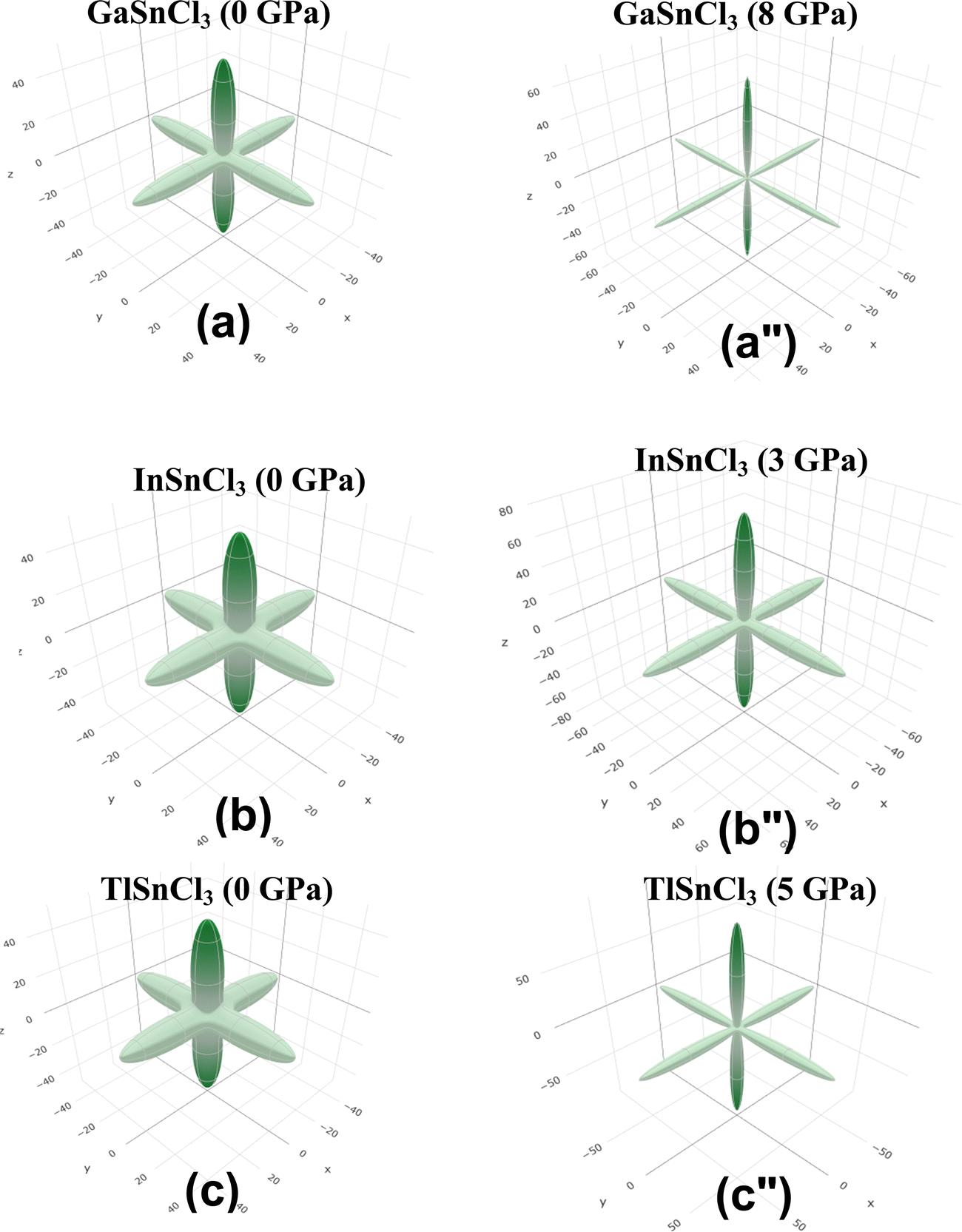 | ||
| Fig. 14 Young's modulus of (a) and (a′′) GaSnCl3, (b) and (b′′) InSnCl3, and (c) and (c′′) TlSnCl3. | ||
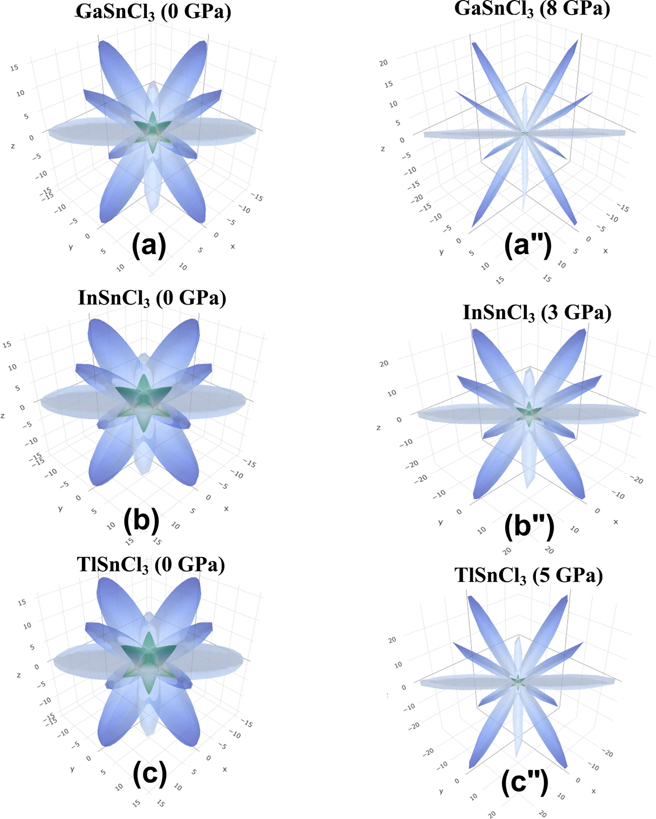 | ||
| Fig. 15 Shear modulus of (a) and (a′′) GaSnCl3, (b) and (b′′) InSnCl3, and (c) and (c′′) TlSnCl3. | ||
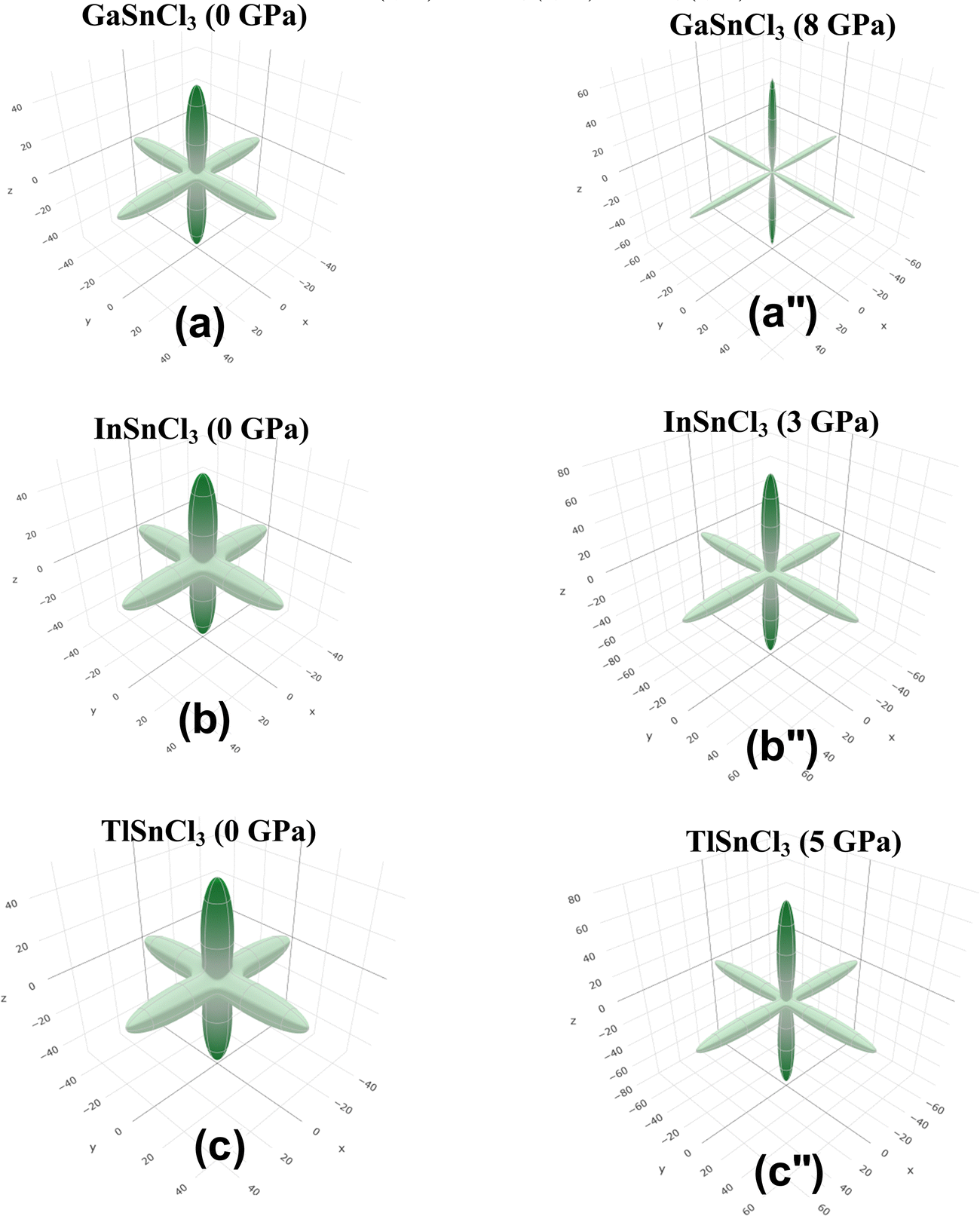 | ||
| Fig. 16 Poisson's ratio of (a) and (a′′) GaSnCl3, (b) and (b′′) InSnCl3, and (c) and (c′′) TlSnCl3. | ||
This analysis involves the calculation and plotting of minimum and maximum values of Young's modulus, shear modulus and Poisson's ratio for ASnCl3 (A = Ga, In, and Tl) compounds in different crystallographic orientations. These values are presented in Table 4 to understand these parameters (v > G > E). The ranking of the three properties, Poisson's ratio (ν), shear modulus (G), and Young's modulus (E), reveals that Poisson's ratio exhibits the highest level of anisotropy, followed by shear modulus, and finally Young's modulus. The 3D illustrations are significant for understanding the variations in elastic properties of the compounds ASnCl3 (A = Ga, In, and Tl) with distinct crystal lattice orientations.
Magnetic properties
A crystal lattice demonstrates diamagnetic properties when two spins are aligned in opposite directions, thus cancelling out each other's spin. Upon examining the graph of the band structure in Fig. 17, it is evident that the ‘α’ and ‘β’ lines overlap with each other. They lie on the same line and, even after rising hydrostatic pressures, they remain in the same overlaid locations. The electron densities of the ASnCl3 (A = Ga, In, and Tl) combination, where almost all of them span a range from −10 eV to 10 eV, are shown in Fig. 18. The ‘α’ and ‘β’ lines correspond to the electron spins, with ‘α’ representing the positive spin and ‘β’ representing the negative spin. The ‘α’ line indicates an upward spin, while the ‘β’ line indicates a downward spin. These two lines exhibit perfect symmetry and are exact reflections of one another. According to the results, the compounds exhibit diamagnetic characteristics when subjected to a magnetic field.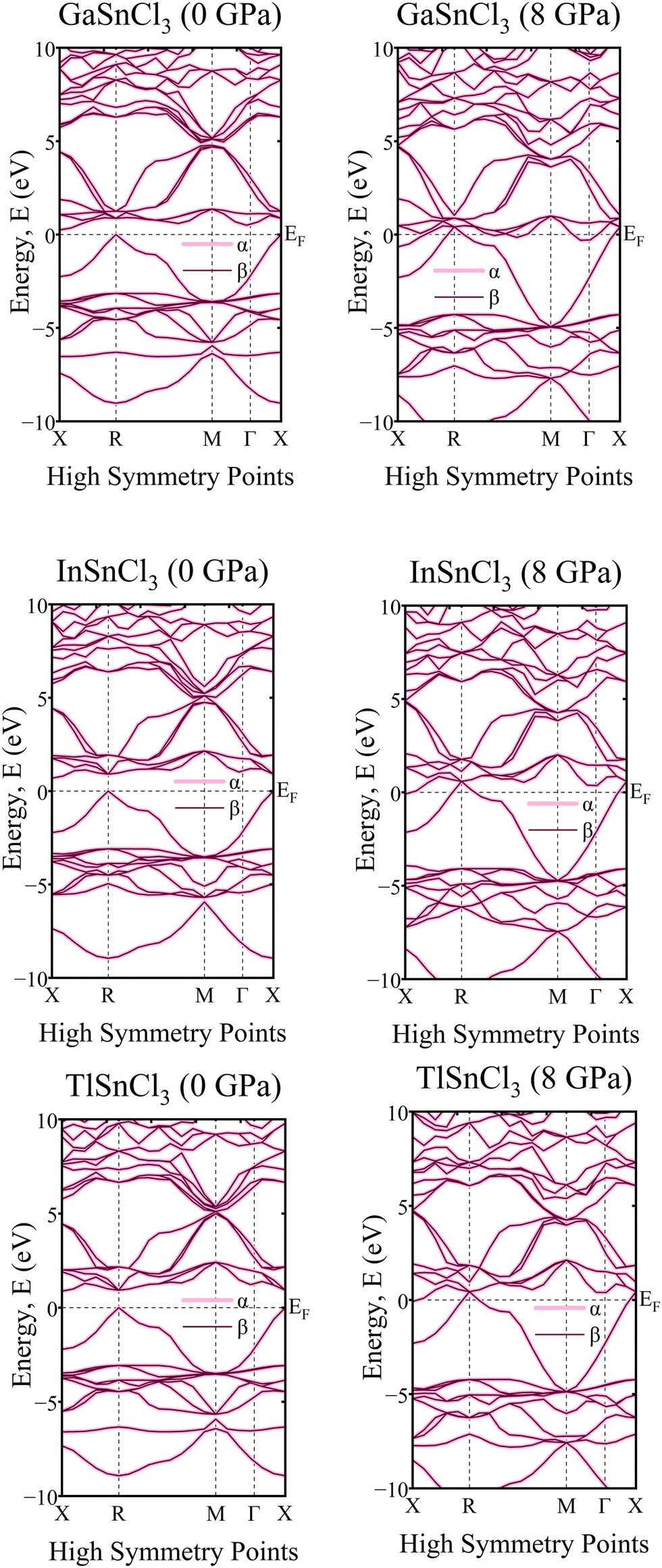 | ||
| Fig. 17 Calculated band structure of ASnCl3 (A = Ga, In, and Tl) with spin-up and spin down channels calculated. | ||
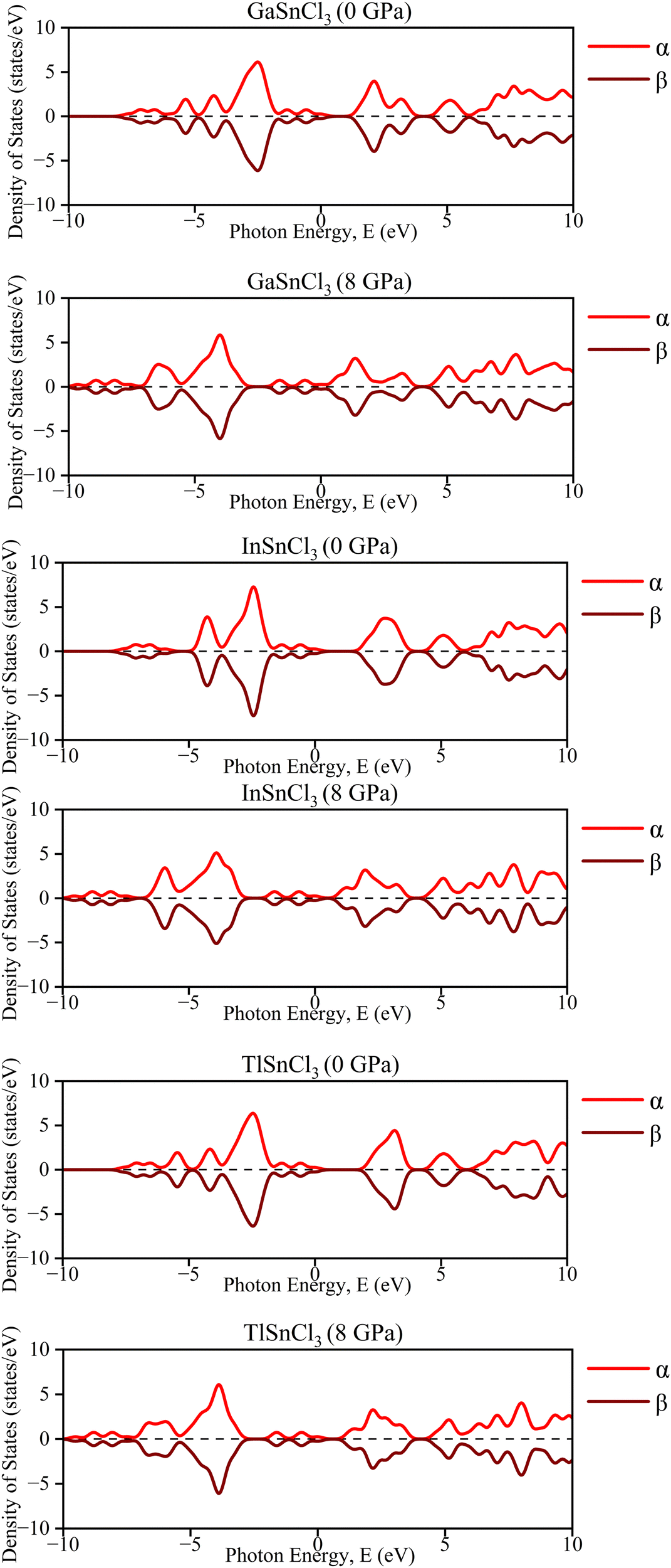 | ||
| Fig. 18 Calculated DOS of ASnCl3 (A = Ga, In, and Tl) with spin-up and down channels. | ||
In the density of states graphs, the number of electrons that may occupy a given state is shown vertically, while their energy level is shown horizontally. Positive DOS refers to states occupied by electrons, whereas negative DOS refers to states filled by holes. As the pressure varies from 0 GPa to 8 GPa, the energy levels of the compounds ASnCl3 (A = Ga, In, and Tl) show negligible fluctuation in the highest peak, but they stay constant across the α and β states of the material. Therefore, the compounds' diamagnetic behavior is unaffected by the application of pressure. No matter how much pressure is applied, the material's magnetic properties will not change.
Thermal properties
A material's thermal properties, which include heat conduction, expansion, and phase transitions, determine temperature changes. Transverse velocity (Vt) denotes the speed at which shear waves, or transverse waves, travel through the materials, moving perpendicular to the direction of propagation. Longitudinal velocity (Vl) denotes the speed at which compressional or longitudinal waves travel, moving in the same direction as the wave's propagation. The mean sound velocity (Vm) is the average velocity at which both transverse and longitudinal waves travel, moving in the velocity at which both transverse and longitudinal sound waves pass through the materials.95 The parameters can be expressed in meters per second (m s−1), with θD denoting the Debye temperature, which is defined as the highest temperature at which the specific heat capacity remains invariant.95 The material's lowest limit of heat conduction is denoted by the minimum thermal conductivity (Kmin), which is mainly determined by phonon transport.96 The phonon thermal conductivity (Kph) refers to the measure of how efficiently heat is transferred through a material via lattice vibrations.79 These two parameters are expressed in watts per meter per kelvin (W m−1 K−1).
Table 5 provides a comprehensive comparison of the thermal properties of the compounds GaSnCl3, InSnCl3, and TlSnCl3 for different applied pressures. For transverse sound velocity (Vt), InSnCl3 generally has the highest values, peaking at 48532.53 m s−1 at 3 GPa, while GaSnCl3Vt decreases from 47061.72 m s−1 at 0 GPa to 42366.7 m s−1 at 8 GPa. TlSnCl3 shows a steady increase in Vt from 43258.14 m s−1 to 43939.8 m s−1 across the pressure range. The longitudinal sound velocity (Vl) increases for all compounds with pressure. TlSnCl3 exhibits the highest Vl at higher pressures, rising from 370646.4 m s−1 at 0 GPa to 585500.4 m s−1 at 8 GPa. In comparison, GaSnCl3 has the lowest Vl, increasing from 298303.7 m s−1 to 466234.6 m s−1 over the same pressure range.
| Compound | Pressure | This work | ||||||
|---|---|---|---|---|---|---|---|---|
| ρ | V t | V l | V m | θ D | K min | K ph | ||
| GaSnCl3 | 0 | 2.85685 | 47061.72 |
298303.7 |
12442.83 |
114.05484 | 0.0162 | 0.968 |
| 2 | 3.07518 | 44912.93 |
345504.8 |
11878.13 |
111.58439 | 0.0163 | 0.653 | |
| 3 | 3.16914 | 44213.66 |
366908.9 |
11694.06 |
110.9629 | 0.0164 | 0.577 | |
| 5 | 3.34227 | 44125.27 |
411542.6 |
11671.69 |
112.7318 | 0.0169 | 0.528 | |
| 6 | 3.41752 | 43608.31 |
429986.7 |
11535.31 |
112.2445 | 0.0170 | 0.489 | |
| 8 | 3.55960 | 42366.7 |
466234.6 |
11207.42 |
110.5448 | 0.0169 | 0.414 | |
| InSnCl3 | 0 | 3.26950 | 48053.36 |
331528.8 |
12706.88 |
116.1872 | 0.0165 | 1.377 |
| 2 | 3.51669 | 48470.21 |
385862 |
12819.38 |
120.0984 | 0.0175 | 1.205 | |
| 3 | 3.62657 | 48532.53 |
412161.4 |
12836.61 |
121.4995 | 0.0179 | 1.129 | |
| 5 | 3.81740 | 48410.34 |
457432.1 |
12805.24 |
123.2923 | 0.0184 | 1.015 | |
| 6 | 3.90020 | 48277.6 |
478309 |
12770.46 |
123.8401 | 0.0187 | 0.965 | |
| 8 | 4.06335 | 47832.31 |
517998.5 |
12653.18 |
124.3904 | 0.0190 | 0.875 | |
| TlSnCl3 | 0 | 4.1186 | 43258.14 |
370646.4 |
11441.64 |
104.5130 | 0.0148 | 1.328 |
| 2 | 4.43180 | 43533.65 |
434218.8 |
11515.63 |
107.7903 | 0.0157 | 1.120 | |
| 3 | 4.56571 | 43806.5 |
463329 |
11588.11 |
109.5506 | 0.0161 | 1.077 | |
| 5 | 4.80816 | 44054.04 |
516258.9 |
11654.03 |
112.0903 | 0.0167 | 1.000 | |
| 6 | 4.91842 | 44060.03 |
540592.6 |
11655.77 |
112.95749 | 0.0170 | 0.963 | |
| 8 | 5.1170 | 43939.8 |
585500.4 |
11624.2 |
114.14765 | 0.0174 | 0.895 | |
Mean sound velocity (Vm) generally decreases with pressure for all compounds, with GaSnCl3 showing the most significant decrease from 12442.83 m s−1 at 0 GPa to 11207.42 m s−1 at 8 GPa. In contrast, InSnCl3 and TlSnCl3 exhibit smaller decreases, with InSnCl3 maintaining the highest Vm throughout. The Debye temperature (D) increases with pressure for InSnCl3 and TlSnCl3, with InSnCl3 having the highest θD, rising from 116.19 K at 0 GPa to 124.39 K at 8 GPa. GaSnCl3D slightly decreases from 114.05 K to 110.54 K, indicating a different response to pressure compared to the other compounds. Minimum thermal conductivity (Kmin) increases slightly for all compounds, with InSnCl3 showing the highest increase from 0.01655 W m−1 K−1 at 0 GPa to 0.01905 W m−1 K−1 at 8 GPa. TlSnCl3 and GaSnCl3 also see increases, though at lower rates. Phonon thermal conductivity (Kph) decreases for all compounds as pressure increases, with InSnCl3 showing the highest initial value of 1.37781 W m−1 K−1 at 0 GPa, which decreases to 0.87508 W m−1 K−1 at 8 GPa. GaSnCl3 shows a more significant decrease, from 0.96832 W m−1 K−1 to 0.41429 W m−1 K−1, indicating a more pronounced reduction in thermal conductivity under pressure.
Phonon analysis
The phonon dispersion curves for GaSnCl3, InSnCl3, and TlSnCl3 provide insights into the vibrational dynamics of these lead-free tin-based halide perovskites, as observed along high-symmetry points in the Brillouin zone (X, R, M, G, and back to R). These curves represent the variation in phonon frequencies (in cm−1) across the Brillouin zone, reflecting the stability and lattice dynamics of the materials. The absence of negative frequencies across all three compounds in Fig. 19 confirms their dynamical stability, indicating that the lattice structures are mechanically stable under ambient conditions. The dispersion plots feature three acoustic branches that start from the gamma (G) point at zero frequency, consistent with translational invariance, and numerous optical branches at higher frequencies, arising from the vibrations of individual atomic sublattices.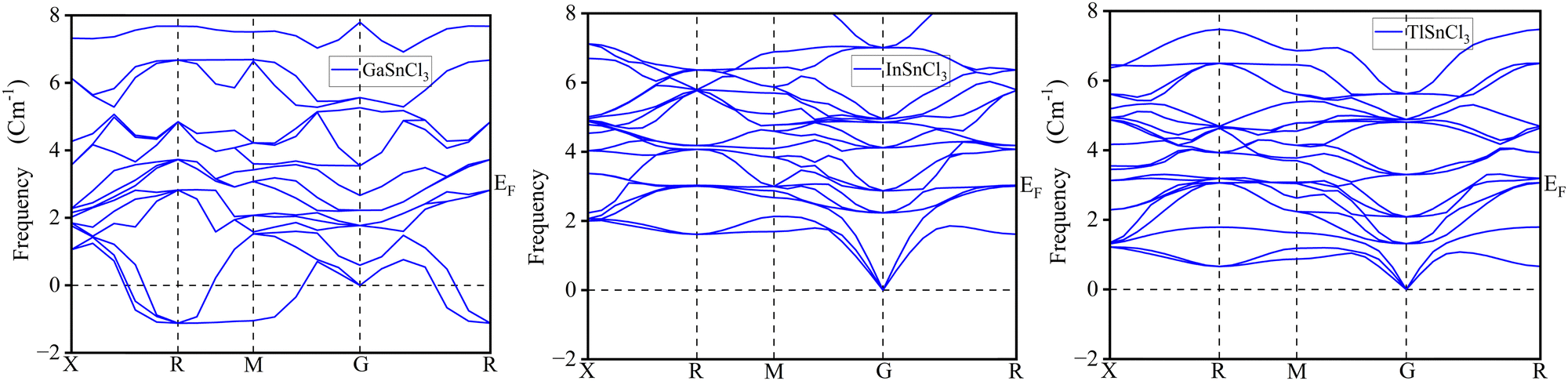 | ||
| Fig. 19 Phonon dispersion curves of GaSnCl3, InSnCl3, and TlSnCl3 perovskites. | ||
For GaSnCl3, the dispersion curves show a distinct separation between the acoustic and optical branches, with the highest optical modes reaching approximately 8 cm−1. This separation suggests a clear distinction in the vibrational modes contributed by the lighter and heavier atoms in the structure. In comparison, the dispersion curves for InSnCl3 and TlSnCl3 exhibit similar frequency ranges but with slightly less pronounced separation between the acoustic and optical branches. The optical branches in InSnCl3 and TlSnCl3 are more distributed, which could be attributed to differences in atomic masses and bonding characteristics within these compounds. The transitions between high-symmetry points, such as X to R, R to M, and M to G, reveal detailed vibrational properties, including mode softening and coupling. These characteristics influence the thermal and mechanical properties of the materials, essential for their application in optoelectronics.
Population analysis
Table 6 provides a detailed analysis of the electronic structure and charge distribution for the compounds GaSnCl3, InSnBr3, and TlSnCl3. This analysis is conducted under two different pressure conditions (0 and 8 GPa) and examines parameters such as charge spilling, Mulliken atomic populations, and charges determined by both Mulliken and Hirshfeld methods.| Compound | Pressure | Charge spilling (%) | Species | Mulliken atomic populations | Mulliken charge | Hirshfeld charge | ||||
|---|---|---|---|---|---|---|---|---|---|---|
| s | p | d | f | Total | ||||||
| GaSnCl3 | 0 | 0.18 | Ga | 1.98 | 0.30 | 10.00 | 0.00 | 12.28 | 0.72 | 0.51 |
| Sn | 1.91 | 1.24 | 10.00 | 0.00 | 13.15 | 0.85 | 0.27 | |||
| Cl | 1.96 | 5.56 | 0.00 | 0.00 | 7.52 | −0.52 | −0.26 | |||
| 8 | 0.24 | Ga | 1.99 | 0.38 | 10.00 | 0.00 | 12.37 | 0.63 | 0.43 | |
| Sn | 1.78 | 1.42 | 10.00 | 0.00 | 13.20 | 0.80 | 0.16 | |||
| Cl | 1.95 | 5.52 | 0.00 | 0.00 | 7.47 | −0.47 | −0.20 | |||
| InSnIn3 | 0 | 0.18 | In | 1.97 | 0.31 | 10.00 | 0.00 | 12.28 | 0.72 | 0.47 |
| Sn | 1.91 | 1.24 | 10.00 | 0.00 | 13.15 | 0.85 | 0.28 | |||
| Cl | 1.96 | 5.56 | 0.00 | 0.00 | 7.52 | −0.52 | −0.25 | |||
| 8 | 0.23 | In | 1.97 | 0.40 | 10.00 | 0.00 | 12.37 | 0.63 | 0.38 | |
| Sn | 1.80 | 1.42 | 10.00 | 0.00 | 13.21 | 0.79 | 0.17 | |||
| Cl | 1.95 | 5.52 | 0.00 | 0.00 | 7.47 | −0.47 | −0.19 | |||
| TlSnCl3 | 0 | 0.15 | Tl | 3.97 | 6.30 | 10.00 | 0.00 | 20.28 | 0.72 | 0.47 |
| Sn | 1.91 | 1.24 | 10.00 | 0.00 | 13.15 | 0.85 | 0.29 | |||
| Cl | 1.96 | 5.56 | 0.00 | 0.00 | 7.52 | −0.52 | −0.25 | |||
| 8 | 0.19 | Tl | 3.96 | 6.39 | 10.00 | 0.00 | 20.35 | 0.65 | 0.39 | |
| Sn | 1.80 | 1.42 | 10.00 | 0.00 | 13.22 | 0.78 | 0.18 | |||
| Cl | 1.95 | 5.52 | 0.00 | 0.00 | 7.48 | −0.48 | −0.19 | |||
The pressure applied in the analysis affects the electronic structure of the compounds, with values provided for 0 and 8 units. Charge spilling refers to the percentage of electron charge not accounted for in Mulliken population analysis, with lower values (below 0.25%) indicating more reliable results. The species column identifies the atom in the compound, while Mulliken atomic populations describe the distribution of electrons across various atomic orbitals (s, p, d, f). The total column sums these orbital populations, measuring each atom's total electron count. The Mulliken charge is the net charge on an atom where a positive value represents electron lost and negative value represents electron gain. Also, the Hirshfeld charge shows the perspective on atomic charge distribution.
At normal ambient pressure, GaSnCl3 shows contribution of the d orbitals with both Ga and Sn atoms, with Mulliken charges of +0.72 and +0.85 respectively. These two orbitals showed partial positive contributions while the Cl atom exhibits −0.52 Mulliken charge as this atom gained electrons. When hydrostatic pressure was applied up to 8 GPa, the Mulliken charge for Ga and Sn atoms decreased to +0.63 and +0.80 respectively, which enhanced the electronic density stability. For InSnCl3 perovskite, the In, Sn and Cl atoms show Mulliken charges of +0.72, +0.85 and −0.52 with Hirshfeld charges of +0.47, +0.28 and −0.25 respectively at 0 GPa pressure. With 8 GPa applied pressure, the charge distribution reduced the positive Mulliken charges for In and Sn, and increased them for Cl which indicates enhanced electronic stability. Similarly, Mulliken and Hirshfeld charges were reduced for Tl and Sn atoms but increased for Cl atoms in the TlSnCl3 perovskite after 8 GPa applied pressure. The low charge density demonstrates the accuracy of the Mulliken charges. Furthermore, increasing pressure results in covalent interaction between atoms and increased stability of the compounds.
Conclusion
This research study offers a brief and comprehensive analysis of the characteristics and attributes of ASnCl3 (A = Ga, In, Tl) perovskites, with Cl as the substituent. The investigation employs density functional theory (DFT) calculations utilizing the CASTEP algorithm. When the hydrostatic pressure reached 8 GPa, the ASnCl3 compound (where, A can be Ga, In, or Tl) saw a decrease in its lattice properties and unit cell volume. The inherent stability of all compounds confirms their mechanical stability. During the mechanical examination, it was shown that ASnCl3 (where A represents Ga, In, or Tl) exhibit greater stiffness and more pronounced elastic anisotropy compared to the other compounds. Analysis of the electronic band structure at 0 GPa indicates that the compound demonstrates semiconductor properties, with a direct band gap observed along specific crystallographic orientations. As the pressure decreases progressively, the band gap increases, resulting in the compound transitioning to a conductive state at various gigapascals (GPa). Through the analysis of increasing pressure based on the analysis of Pugh's ratio and Poisson's ratio, it is shown that ASnCl3 compounds (where, A represents Ga, In, Tl) are inclined towards increased ductility. These materials have the potential to be useful in circumstances where a high level of ductility is necessary for practical application. Upon optical investigation, it was shown that ASnCl3 compounds (where, A represents Ga, In, or Tl) exhibited higher absorptivity, photoconductivity, and loss function in the ultraviolet (UV) region compared to the other compounds. The Mulliken atomic population and Hirshfeld charge analyses demonstrated significant alterations in atomic populations under pressure, particularly for Sn and Cl atoms. This suggests the possibility of modifiable electrical properties. The compounds exhibited diamagnetic characteristics, providing additional evidence for the suitability of ASnCl3 (A = Ga, In, Tl) as an environmentally friendly inorganic perovskite material for high-performance solar cells and diverse optoelectronic applications, especially in devices that are responsive to ultraviolet radiation.Author contributions
Md Ratul Hasan contributed to methodology, data curation, and formal analysis, writing the original draft; Imtiaz Ahamed Apon contributed to formal analysis, conceptualization, formal analysis, writing the original draft and reviewing and editing of the manuscript; Md. Mafidul Islam, Asab Uzzaman Azad, and Md. Solayman contributed to data curation, reviewing and editing of the manuscript; Md. Salman Haque helped with supervision and formal analysis throughout the whole research project.Compliance with ethical standards
All procedures were performed following ethical standards.Data availability
The data that support the findings of this study are available on request from the corresponding author.Conflicts of interest
The authors declare that they have no competing interests.Acknowledgements
We declare that this research is not supported or funded by any organization or individual.References
- E. A. Katz, Perovskite: Name Puzzle and German-Russian Odyssey of Discovery, Helv. Chim. Acta, 2020, 103, e2000061, DOI:10.1002/hlca.202000061.
- T. Leijtens, G. E. Eperon, N. K. Noel, S. N. Habisreutinger, A. Petrozza and H. J. Snaith, Stability of Metal Halide Perovskite Solar Cells, Adv. Energy Mater., 2015, 5, 1500963, DOI:10.1002/aenm.201500963.
- N. Erum and M. A. Iqbal, Ab initio study of high dielectric constant oxide-perovskites: perspective for miniaturization technology, Mater. Res. Express, 2017, 4, 025904, DOI:10.1088/2053-1591/aa5d8d.
- D. Zhang, S. W. Eaton, Y. Yu, L. Dou and P. Yang, Solution-Phase Synthesis of Cesium Lead Halide Perovskite Nanowires, J. Am. Chem. Soc., 2015, 137, 9230–9233, DOI:10.1021/jacs.5b05404.
- M. Saiduzzaman, T. Takei, S. Yanagida, N. Kumada, H. Das, H. Kyokane, S. Wakazaki, M. Azuma, C. Moriyoshi and Y. Kuroiwa, Hydrothermal Synthesis of Pyrochlore-Type Pentavalent Bismuthates Ca2Bi2O7 and Sr2Bi2O7, Inorg. Chem., 2019, 58, 1759–1763, DOI:10.1021/acs.inorgchem.8b03596.
- M. Saiduzzaman, H. Yoshida, T. Takei, S. Yanagida, N. Kumada, M. Nagao, H. Yamane, M. Azuma, M. H. K. Rubel, C. Moriyoshi and Y. Kuroiwa, Hydrothermal Synthesis and Crystal Structure of a (Ba0.54K0.46)4Bi4O12 Double-Perovskite Superconductor with Onset of the Transition Tc ∼ 30 K, Inorg. Chem., 2019, 58, 11997–12001, DOI:10.1021/acs.inorgchem.9b01768.
- C. Gómez-Solís, J. Oliva, L. A. Diaz-Torres, J. Bernal-Alvarado, V. Reyes-Zamudio, A. Abidov and L. M. Torres-Martinez, Efficient photocatalytic activity of MSnO3 (M: Ca, Ba, Sr) stannates for photoreduction of 4-nitrophenol and hydrogen production under UV light irradiation, J. Photochem. Photobiol., A, 2019, 371, 365–373, DOI:10.1016/j.jphotochem.2018.11.039.
- W. Dong, B. Li, Y. Li, X. Wang, L. An, C. Li, B. Chen, G. Wang and Z. Shi, General Approach to Well-Defined Perovskite MTiO 3 (M = Ba, Sr, Ca, and Mg) Nanostructures, J. Phys. Chem. C, 2011, 115, 3918–3925, DOI:10.1021/jp110660v.
- V. V. Lemanov, A. V. Sotnikov, E. P. Smirnova, M. Weihnacht and R. Kunze, Perovskite CaTiO3 as an incipient ferroelectric, Solid State Commun., 1999, 110, 611–614, DOI:10.1016/S0038-1098(99)00153-2.
- J. Jia, S. Guo, S. Yan, F. Cao, C. Yao, X. Dong and G. Wang, Simultaneous large pyroelectric response and high depolarization temperature in sodium bismuth titanate-based perovskites, Appl. Phys. Lett., 2019, 114, 032902, DOI:10.1063/1.5063318.
- K. Wieczorek, A. Ziebiniska, Z. Ujma, K. Szot, M. Górny, I. Franke, J. Koperski, A. Soszyński and K. Roleder, Electrostrictive and Piezoelectric Effect in BaTiO3 and PbZrO3, Ferroelectrics, 2006, 336, 61–67, DOI:10.1080/00150190600695743.
- R. M. Kusters, J. Singleton, D. A. Keen, R. McGreevy and W. Hayes, Magnetoresistance measurements on the magnetic semiconductor Nd0.5Pb0.5MnO3, Phys. B, 1989, 155, 362–365, DOI:10.1016/0921-4526(89)90530-9.
- L. M. Feng, L. Q. Jiang, M. Zhu, H. B. Liu, X. Zhou and C. H. Li, Formability of ABO3 cubic perovskites, J. Phys. Chem. Solids, 2008, 69, 967–974, DOI:10.1016/j.jpcs.2007.11.007.
- H. Hayashi, Structural consideration on the ionic conductivity of perovskite-type oxides, Solid State Ionics, 1999, 122, 1–15, DOI:10.1016/S0167-2738(99)00066-1.
- A. Oleaga, A. Salazar and D. Skrzypek, Critical behaviour of magnetic transitions in KCoF3 and KNiF3 perovskites, J. Alloys Compd., 2015, 629, 178–183, DOI:10.1016/j.jallcom.2014.12.237.
- M. Awais Rehman, J. Ur Rehman and M. Bilal Tahir, A DFT study of structural, electronic, optical, mechanical, thermoelectric, and magnetic properties of Pb-halide perovskites LiPbX3 (X = Cl, Br, and I) for photovoltaic applications, Comput. Theor. Chem., 2023, 1223, 114085, DOI:10.1016/j.comptc.2023.114085.
- M. U. Ghani, M. Sagir, M. B. Tahir and S. Ullah, Evaluation of structural, electronic, optical, mechanical, and thermodynamic properties of LiXCl3 (X = Sn, Pb) for solar cell applications: first-principles approach, Opt. Quantum Electron., 2024, 56, 1292, DOI:10.1007/s11082-024-07212-x.
- Y. Selmani, H. Labrim and L. Bahmad, Structural, optoelectronic and thermoelectric properties of the new perovskites LiMCl3 (M = Pb or Sn): a DFT study, Opt. Quantum Electron., 2024, 56, 1416, DOI:10.1007/s11082-024-07319-1.
- A. R. Fajarini Sidik, P. Pitriana and H. Aliah, Absorbance Optical Properties Calculation of ABX3 (A = Cs, Li; B = Pb; X = I, Br, Cl) Cubic Phase Using Density Functional Theory (DFT) Method, KLS, 2024, 275–283, DOI:10.18502/kls.v8i1.15591.
- S. Khan, N. Mehmood, R. Ahmad, A. Kalsoom and K. Hameed, Analysis of structural, elastic and optoelectronic properties of indium-based halide perovskites InACl3 (A = Ge, Sn, Pb) using density functional theory, Mater. Sci. Semicond. Process., 2022, 150, 106973, DOI:10.1016/j.mssp.2022.106973.
- R. Nie, R. R. Sumukam, S. H. Reddy, M. Banavoth and S. I. Seok, Lead-free perovskite solar cells enabled by hetero-valent substitutes, Energy Environ. Sci., 2020, 13, 2363–2385, 10.1039/D0EE01153C.
- M. Llanos, R. Yekani, G. P. Demopoulos and N. Basu, Alternatives assessment of perovskite solar cell materials and their methods of fabrication, Renewable Sustainable Energy Rev., 2020, 133, 110207, DOI:10.1016/j.rser.2020.110207.
- N. H. Linh, N. H. Tuan, D. D. Dung, P. Q. Bao, B. T. Cong and L. T. H. Thanh, Alkali metal-substituted bismuth-based perovskite compounds: a DFT study, J. Sci.: Adv. Mater. Dev., 2019, 4, 492–498, DOI:10.1016/j.jsamd.2019.06.005.
- G. Murtaza, I. Ahmad and A. Afaq, Shift of indirect to direct bandgap in going from K to Cs in MCaF3 (M = K, Rb, Cs), Solid State Sci., 2013, 16, 152–157, DOI:10.1016/j.solidstatesciences.2012.10.002.
- M. R. Molla, M. Saiduzzaman, T. I. Asif, W. A. Dujana and K. M. Hossain, Electronic phase transition from semiconducting to metallic in cubic halide CsYbCl3 perovskite under hydrostatic pressure, Phys. B, 2022, 630, 413650, DOI:10.1016/j.physb.2021.413650.
- B. Wu, W. Ning, Q. Xu, M. Manjappa, M. Feng, S. Ye, J. Fu, S. Lie, T. Yin, F. Wang, T. W. Goh, P. C. Harikesh, Y. K. E. Tay, Z. X. Shen, F. Huang, R. Singh, G. Zhou, F. Gao and T. C. Sum, Strong self-trapping by deformation potential limits photovoltaic performance in bismuth double perovskite, Sci. Adv., 2021, 7, eabd3160, DOI:10.1126/sciadv.abd3160.
- Z. Lan, J. Meng, K. Zheng and I. E. Castelli, Exploring the Intrinsic Point Defects in Cesium Copper Halides, J. Phys. Chem. C, 2021, 125, 1592–1598, DOI:10.1021/acs.jpcc.0c11216.
- D. Moghe, L. Wang, C. J. Traverse, A. Redoute, M. Sponseller, P. R. Brown, V. Bulović and R. R. Lunt, All vapor-deposited lead-free doped CsSnBr3 planar solar cells, Nano Energy, 2016, 28, 469–474, DOI:10.1016/j.nanoen.2016.09.009.
- S. J. Clark, C. D. Flint and J. D. Donaldson, Luminescence and electrical conductivity of CsSnBr3, and related phases, J. Phys. Chem. Solids, 1981, 42, 133–135, DOI:10.1016/0022-3697(81)90072-X.
- J.-C. Zheng, C. H. A. Huan, A. T. S. Wee and M. H. Kuok, Electronic properties of CsSnBr3: studies by experiment and theory, Surf. Interface Anal., 1999, 28, 81–83, DOI:10.1002/(SICI)1096-9918(199908)28:1
![[double bond splayed right]](https://www.rsc.org/images/entities/char_e00a.gif) 81::AID-SIA623
81::AID-SIA623![[double bond splayed left]](https://www.rsc.org/images/entities/char_e009.gif) 3.0.CO;2-D.
3.0.CO;2-D. - L. Huang and W. R. L. Lambrecht, Electronic band structure, phonons, and exciton binding energies of halide perovskites CsSnCl3, CsSnBr3, and CsSnI3, Phys. Rev. B: Condens. Matter Mater. Phys., 2013, 88, 165203, DOI:10.1103/PhysRevB.88.165203.
- M. Houari, B. Bouadjemi, S. Haid, M. Matougui, T. Lantri, Z. Aziz, S. Bentata and B. Bouhafs, Semiconductor behavior of halide perovskites AGeX3 (A = K, Rb and Cs; X = F, Cl and Br): first-principles calculations, Indian J. Phys., 2020, 94, 455–467, DOI:10.1007/s12648-019-01480-0.
- M. I. Kholil, M. T. H. Bhuiyan, M. A. Rahman, M. S. Ali and M. Aftabuzzaman, Influence of molybdenum and technetium doping on visible light absorption, optical and electronic properties of lead-free perovskite CsSnBr3 for optoelectronic applications, RSC Adv., 2021, 11, 2405–2414, 10.1039/D0RA09853A.
- R. Yadav, A. Srivastava, J. A. Abraham, R. Sharma and S. A. Dar, First-principles calculations to investigate structural, electronic, thermoelectric, and optical properties of heavy thallium perovskite TlPbX3 (X = Cl, Br, I), Mater. Sci. Eng., B, 2022, 283, 115781, DOI:10.1016/j.mseb.2022.115781.
- M. Tyagi, M. Zhuravleva and C. L. Melcher, Theoretical and experimental characterization of promising new scintillators: Eu2+ doped CsCaCl3 and CsCaI3, J. Appl. Phys., 2013, 113, 203504, DOI:10.1063/1.4807401.
- J. Grimm, J. F. Suyver, E. Beurer, G. Carver and H. U. Güdel, Light-Emission and Excited-State Dynamics in Tm2+ Doped CsCaCl3, CsCaBr3, and CsCaI3, J. Phys. Chem. B, 2006, 110, 2093–2101, DOI:10.1021/jp055930p.
- Z. Md and A. K. M. Rahaman, Akther Hossain, Effect of metal doping on the visible light absorption, electronic structure and mechanical properties of non-toxic metal halide CsGeCl3, RSC Adv., 2018, 8, 33010–33018, 10.1039/C8RA06374E.
- J. Islam and A. K. M. A. Hossain, Narrowing band gap and enhanced visible-light absorption of metal-doped non-toxic CsSnCl3 metal halides for potential optoelectronic applications, RSC Adv., 2020, 10, 7817–7827, 10.1039/C9RA10407K.
- Md. A. Rahman, F. Mostari, Md. Z. Hasan, A. Irfan, Md. F. Rahman, M. J. Hosain, S. C. Mouna, I. A. Chowdhury, Md Rasheduzzaman and M. S. H. Choudhury, First principles study on the structural, elastic, electronic, optical and thermal properties of lead-free perovskites CsCaX3 (X = F, Cl, Br), Phys. B, 2023, 669, 415260, DOI:10.1016/j.physb.2023.415260.
- Z. Jellil and H. Ez-Zahraouy, Pressure-induced band gap engineering and enhanced optoelectronic properties of non-toxic Ca-based perovskite CsCaCl3: insights from density functional theory, Comput. Condens. Matter, 2024, 38, e00879, DOI:10.1016/j.cocom.2024.e00879.
- A. M. Asiri, M. K. Shahzad, S. Hussain, K. Zhu, S. B. Khan, K. A. Alamry, S. Y. Alfifi and H. M. Marwani, Analysis of XGaO3 (X = Ba and Cs) cubic based perovskite materials for photocatalytic water splitting applications: a DFT study, Heliyon, 2023, 9, e14112, DOI:10.1016/j.heliyon.2023.e14112.
- V. Shivhare, S. A. Khandy and D. C. Gupta, Probing the structural, mechanical, phonon, thermal, and transport properties of magnetic halide perovskites XTiBr3 (X = Rb, Cs) through ab-initio results, Sci. Rep., 2023, 13, 9115, DOI:10.1038/s41598-023-34047-5.
- M. Rashid, N. A. Noor, B. Sabir, S. Ali, M. Sajjad, F. Hussain, N. U. Khan, B. Amin and R. Khenata, Ab initio study of fundamental properties of ternary ZnO1−xSx alloys by using special quasi-random structures, Comput. Mater. Sci., 2014, 91, 285–291, DOI:10.1016/j.commatsci.2014.04.032.
- M. Hassan, I. Arshad and Q. Mahmood, Computational study of electronic, optical and thermoelectric properties of X3PbO (X = Ca, Sr, Ba) anti-perovskites, Semicond. Sci. Technol., 2017, 32, 115002, DOI:10.1088/1361-6641/aa8afe.
- S. S. A. Gillani, R. Ahmad, M. Rizwan, M. Rafique, G. Ullah, C. B. Cao and H. B. Jin, Effect of magnesium doping on band gap and optical properties of SrZrO3 perovskite: a first-principles study, Optik, 2019, 191, 132–138, DOI:10.1016/j.ijleo.2019.05.099.
- S. S. A. Gillani, R. Ahmad, I. Zeba, Islah-u-din, M. Rizwan, M. Rafique, M. Shakil, S. Jabbar and M. Siddique, Structural stability of SrZrO3 perovskite and improvement in electronic and optical properties by Ca and Ba doping for optoelectronic applications: a DFT approach, Philos. Mag., 2019, 99, 3133–3145, DOI:10.1080/14786435.2019.1663955.
- M. Saiduzzaman, T. Takei and N. Kumada, Hydrothermal magic for the synthesis of new bismuth oxides, Inorg. Chem. Front., 2021, 8, 2918–2938, 10.1039/D1QI00337B.
- N. A. Noor, M. Rashid, S. M. Alay-e-Abbas, M. Raza, A. Mahmood, S. M. Ramay and G. Murtaza, Shift of indirect to direct bandgap and thermoelectric response of the cubic BiScO3 via DFT-mBJ studies, Mater. Sci. Semicond. Process., 2016, 49, 40–47, DOI:10.1016/j.mssp.2016.03.014.
- A. Batool, M. A. Faridi, Q. Mahmood, B. Ul Haq, A. Laref and S. E. Awan, The pressure-induced indirect to direct bandgap transition and thermoelectric response in SrTiO3: an ab initio study, J. Phys. Chem. Solids, 2018, 123, 70–75, DOI:10.1016/j.jpcs.2018.07.008.
- N. A. Noor, M. Rashid, G. M. Mustafa, M. I. Khan, A. Mahmood and S. M. Ramay, Study of pressure induced physical properties of ZnZrO3 perovskite using density functional theory, Chem. Phys. Lett., 2020, 753, 137601, DOI:10.1016/j.cplett.2020.137601.
- M. Yaseen, M. K. Butt, A. Ashfaq, J. Iqbal, M. M. Almoneef, Misbah, M. Iqbal, A. Murtaza and A. Laref, Phase transition and thermoelectric properties of cubic KNbO3 under pressure: DFT approach, J. Mater. Res. Technol., 2021, 11, 2106–2113, DOI:10.1016/j.jmrt.2021.02.017.
- M. Yaseen, H. Shafiq, J. Iqbal, Misbah, F. Batool, A. Murtaza, M. Iqbal, H. Althib, S. M. Ramay and A. Mahmood, Pressure induced electronic, optical and thermoelectric properties of cubic SrZrO3: DFT investigation, Phys. B, 2021, 612, 412626, DOI:10.1016/j.physb.2020.412626.
- N. A. Noor, Q. Mahmood, M. Rashid, B. Ul Haq and A. Laref, The pressure-induced mechanical and optoelectronic behavior of cubic perovskite PbSnO3 via ab initio investigations, Ceram. Int., 2018, 44, 13750–13756, DOI:10.1016/j.ceramint.2018.04.217.
- J. Islam and A. K. M. A. Hossain, Semiconducting to metallic transition with outstanding optoelectronic properties of CsSnCl3 perovskite under pressure, Sci. Rep., 2020, 10, 14391, DOI:10.1038/s41598-020-71223-3.
- M. I. Kholil and M. T. H. Bhuiyan, Effects of pressure on narrowing the band gap, visible light absorption, and semi-metallic transition of lead-free perovskite CsSnBr3 for optoelectronic applications, J. Phys. Chem. Solids, 2021, 154, 110083, DOI:10.1016/j.jpcs.2021.110083.
- M. A. Islam, Md. Z. Rahaman and S. K. Sen, A comparative study of hydrostatic pressure treated environmentally friendly perovskites CsXBr3 (X = Ge/Sn) for optoelectronic applications, AIP Adv., 2021, 11, 075109, DOI:10.1063/5.0057287.
- M. A. Islam, J. Islam, M. N. Islam, S. K. Sen and A. K. M. A. Hossain, Enhanced ductility and optoelectronic properties of environment-friendly CsGeCl3 under pressure, AIP Adv., 2021, 11, 045014, DOI:10.1063/5.0048849.
- Md. S. Hossain, Md. M. Haque Babu, T. Saha, Md. S. Hossain, J. Podder, Md. S. Rana, A. Barik and P. Rani, Pressure induced semiconductor to metal phase transition in cubic CsSnBr3 perovskite, AIP Adv., 2021, 11, 055024, DOI:10.1063/5.0048979.
- Q. A. Akkerman, V. D’Innocenzo, S. Accornero, A. Scarpellini, A. Petrozza, M. Prato and L. Manna, Tuning the Optical Properties of Cesium Lead Halide Perovskite Nanocrystals by Anion Exchange Reactions, J. Am. Chem. Soc., 2015, 137, 10276–10281, DOI:10.1021/jacs.5b05602.
- M. Roknuzzaman, K. Ostrikov, H. Wang, A. Du and T. Tesfamichael, Towards lead-free perovskite photovoltaics and optoelectronics by ab initio simulations, Sci. Rep., 2017, 7, 14025, DOI:10.1038/s41598-017-13172-y.
- T. A. Geleta, D. Behera, N. Bouri, V. J. R. Rivera and F. M. Gonzalo, First principles insight into the study of the structural, stability, and optoelectronic properties of alkali-based single halide perovskite ZSnCl3 (Z = Na/K) materials for photovoltaic applications, J. Comput. Chem., 2024, 45(30), 2574–2586, DOI:10.1002/jcc.27465.
- I. A. Ovi, M. R. Hasan, I. A. Apon and F.-T. Zahra, The structural, magnetic, optoelectronic, and mechanical characteristics of NaGeX3 perovskites under pressure for soler-cell applications, Mater. Res. Express, 2024, 11, 065904, DOI:10.1088/2053-1591/ad594d.
- M. Ullah, R. Neffati, G. Murtaza, S. Khan, M. Haneef and M. W. Ashraf, Pressure induced variations in the optoelectronic response of ASnX3 (A = K, Rb; X = Cl, Br, I) perovskites: a first principles study, Mater. Sci. Semicond. Process., 2022, 150, 106977, DOI:10.1016/j.mssp.2022.106977.
- M. A. Rashid, M. Saiduzzaman, A. Biswas and K. M. Hossain, First-principles calculations to explore the metallic behavior of semiconducting lead-free halide perovskites RbSnX3 (X = Cl, Br) under pressure, Eur. Phys. J. Plus, 2022, 137, 649, DOI:10.1140/epjp/s13360-022-02843-z.
- O. Das, M. Saiduzzaman, K. M. Hossain, I. K. Shuvo, M. M. Rahman, S. Ahmad and S. K. Mitro, First-principles calculations to investigate pressure-driven electronic phase transition of lead-free halide perovskites KMCl3 (M = Ge, Sn) for superior optoelectronic performance, Results Phys., 2023, 44, 106212, DOI:10.1016/j.rinp.2023.106212.
- S. Yalameha, P. Saeidi, Z. Nourbakhsh, A. Vaez and A. Ramazani, Insight into the topological phase and elastic properties of halide perovskites CsSnX3 (X = l, Br, Cl) under hydrostatic pressures, J. Appl. Phys., 2020, 127, 085102, DOI:10.1063/1.5125920.
- I. A. Apon, M. D. Ratul Hasan, I. A. Ovi and Fatema-Tuz-Zahra, Pressure-driven semiconducting to metallic transition in francium tin trihalides perovskite with improved optoelectronic performance: a DFT study, AIP Adv., 2024, 14, 065126, DOI:10.1063/5.0207336.
- M. D. R. Hasan, I. A. Apon, I. A. Ovi and M. S. Haque, Calculations of the mechanical, optoelectronic, and magnetic properties of FrGeX3 (X = Cl, Br, I) under hydrostatic pressures based on first-principles theories, AIP Adv., 2024, 14, 035341, DOI:10.1063/5.0201448.
- J. K. Rony, M. Islam, M. Saiduzzaman, K. M. Hossain, S. Alam, A. Biswas, M. H. Mia, S. Ahmad and S. K. Mitro, TlBX3 (B = Ge, Sn; X = Cl, Br, I): promising non-toxic metal halide perovskites for scalable and affordable optoelectronics, J. Mater. Res. Technol., 2024, 29, 897–909, DOI:10.1016/j.jmrt.2024.01.093.
- R. K. Pingak, S. Bouhmaidi, A. Harbi, L. Setti, F. Nitti, M. Moutaabbid, A. Z. Johannes, N. U. J. Hauwali and M. Z. Ndii, A DFT investigation of lead-free TlSnX3 (X = Cl, Br, or I) perovskites for potential applications in solar cells and thermoelectric devices, RSC Adv., 2023, 13, 33875–33886, 10.1039/D3RA06685A.
- P. Sharma, P. Ranjan and T. Chakraborty, Study of Tl-based perovskite materials TlZX3 (Z = Ge, Sn, Be, Sr; X = Cl, Br, I) for application in scintillators: DFT and TD-DFT approach, Chem. Phys. Impact, 2023, 7, 100344, DOI:10.1016/j.chphi.2023.100344.
- R. K. Pingak, A. Harbi, M. Moutaabbid, A. Z. Johannes, N. U. J. Hauwali, M. Bukit, F. Nitti and M. Z. Ndii, Lead-free perovskites InSnX3 (X = Cl, Br, I) for solar cell applications: a DFT study on the mechanical, optoelectronic, and thermoelectric properties, Mater. Res. Express, 2023, 10, 095507, DOI:10.1088/2053-1591/acf984.
- P. Ch Sahu and N. V. Chandra Shekar, High pressure research on materials: 2. Experimental techniques to study the behaviour of materials under high pressure, Reson, 2007, 12, 49–64, DOI:10.1007/s12045-007-0082-6.
- W. Kim, B. Koo, M. J. Ko and H. Jung, Hot-injection synthesis of lead-free pseudo-alkali metal-based perovskite (TlSnX3) nanoparticles with tunable optical properties, Front. Mater., 2023, 10, 1298188, DOI:10.3389/fmats.2023.1298188.
- H. Yao, F. Zhou, Z. Li, Z. Ci, L. Ding and Z. Jin, Strategies for Improving the Stability of Tin-Based Perovskite (ASnX3) Solar Cells, Adv. Sci., 2020, 7, 1903540, DOI:10.1002/advs.201903540.
- W. Zhuang and J. Song, Thallium in aquatic environments and the factors controlling Tl behavior, Environ. Sci. Pollut. Res., 2021, 28, 35472–35487, DOI:10.1007/s11356-021-14388-2.
- Md. S. Ali, S. Das, Y. F. Abed and M. A. Basith, Lead-free CsSnCl3 perovskite nanocrystals: rapid synthesis, experimental characterization and DFT simulations, Phys. Chem. Chem. Phys., 2021, 23, 22184–22198, 10.1039/D1CP02666F.
- K. Sakamoto, T. Oda, A. Kimura, Y. Takeichi, J. Fujii, R. I. G. Uhrberg, M. Donath and H. W. Yeom, Symmetry induced peculiar Rashba effect on thallium adsorbed Si(1 1 1) surfaces, J. Electron Spectrosc. Relat. Phenom., 2015, 201, 88–91, DOI:10.1016/j.elspec.2014.09.008.
- S. J. Clark, M. D. Segall, C. J. Pickard, P. J. Hasnip, M. I. J. Probert, K. Refson and M. C. Payne, First principles methods using CASTEP, Z. Kristallogr. – Cryst. Mater., 2005, 220, 567–570, DOI:10.1524/zkri.220.5.567.65075.
- D. Vanderbilt, Soft self-consistent pseudopotentials in a generalized eigenvalue formalism, Phys. Rev. B: Condens. Matter Mater. Phys., 1990, 41, 7892–7895, DOI:10.1103/PhysRevB.41.7892.
- J. P. Perdew, K. Burke and M. Ernzerhof, Generalized Gradient Approximation Made Simple, Phys. Rev. Lett., 1996, 77, 3865–3868, DOI:10.1103/PhysRevLett.77.3865.
- Md. S. Islam, Md. A. Rahman and M. S. Ali, Influence of pressure on the different physical features of lead-free double perovskite materials K2SnX6 (X = Cl, and Br): DFT replication, Solid State Commun., 2024, 392, 115652, DOI:10.1016/j.ssc.2024.115652.
- S. A. Khattak, S. M. Wabaidur, A. A. Alothman, M. Husain, M. A. Ali, N. Rahman, I. Ullah, S. Zulfiqar, G. Rooh, T. Khan and G. Khan, DFT study of structural, elastic and optoelectronic characteristics of novel Rb2CaSnX6 (X = Cl, I) double halide perovskites for optoelectronic applications, Opt. Quantum Electron., 2024, 56, 1384, DOI:10.1007/s11082-024-07318-2.
- Md. M. H. Babu, T. Saha, J. Podder, P. Roy, A. Barik and E. Haque, Electronic structure transition of cubic CsSnCl3 under pressure: effect of rPBE and PBEsol functionals and GW method, Heliyon, 2021, 7, e07796, DOI:10.1016/j.heliyon.2021.e07796.
- T. C. Jellicoe, J. M. Richter, H. F. J. Glass, M. Tabachnyk, R. Brady, S. E. Dutton, A. Rao, R. H. Friend, D. Credgington, N. C. Greenham and M. L. Böhm, Synthesis and Optical Properties of Lead-Free Cesium Tin Halide Perovskite Nanocrystals, J. Am. Chem. Soc., 2016, 138, 2941–2944, DOI:10.1021/jacs.5b13470.
- J. Barrett, S. R. A. Bird, J. D. Donaldson and J. Silver, The Mössbauer effect in tin(II) compounds. Part XI. The spectra of cubic trihalogenostannates(II), J. Chem. Soc. A, 1971, 3105–3108, 10.1039/J19710003105.
- K. Khan, J. Sahariya and A. Soni, Structural, electronic and optical modeling of perovskite solar materials ASnX3 (A = Rb, K; X = Cl, Br): first principle investigations, Mater. Chem. Phys., 2021, 262, 124284, DOI:10.1016/j.matchemphys.2021.124284.
- Md. H. Rahman, Md Jubair, Md. Z. Rahaman, Md. S. Ahasan, K. (Ken) Ostrikov and M. Roknuzzaman, RbSnX3 (X = Cl, Br, I): promising lead-free metal halide perovskites for photovoltaics and optoelectronics, RSC Adv., 2022, 12, 7497–7505, 10.1039/D2RA00414C.
- N. Hasan, M. Arifuzzaman and A. Kabir, Structural, elastic and optoelectronic properties of inorganic cubic FrBX3 (B = Ge, Sn; X = Cl, Br, I) perovskite: the density functional theory approach, RSC Adv., 2022, 12, 7961–7972, 10.1039/D2RA00546H.
- S. K. Mitro, M. Saiduzzaman, T. I. Asif and K. M. Hossain, Band gap engineering to stimulate the optoelectronic performance of lead-free halide perovskites RbGeX3 (X = Cl, Br) under pressure, J. Mater. Sci.: Mater. Electron., 2022, 33, 13860–13875, DOI:10.1007/s10854-022-08318-2.
- M. A. Haq, M. Saiduzzaman, T. I. Asif, I. K. Shuvo and K. M. Hossain, Ultra-violet to visible band gap engineering of cubic halide KCaCl3 perovskite under pressure for optoelectronic applications: insights from DFT, RSC Adv., 2021, 11, 36367–36378, 10.1039/D1RA06430D.
- S. Ando, DFT Calculations on Refractive Index Dispersion of Fluoro-compounds in the DUV-UV-Visible Region, J. Photopol. Sci. Technol., 2006, 19, 351–360, DOI:10.2494/photopolymer.19.351.
- Md. Z. Hasan, K. M. Hossain, S. K. Mitro, Md Rasheduzzaman, J. K. Modak and M. A. Rayhan, Structural, mechanical, electronic, and anisotropic properties of niobium-doped strontium ferrite: first-principle calculations, Appl. Phys. A: Mater. Sci. Process., 2021, 127, 36, DOI:10.1007/s00339-020-04219-5.
- B. Shafiro and M. Kachanov, Anisotropic effective conductivity of materials with nonrandomly oriented inclusions of diverse ellipsoidal shapes, J. Appl. Phys., 2000, 87, 8561–8569, DOI:10.1063/1.373579.
- Q. Chen and B. Sundman, Calculation of debye temperature for crystalline structures—a case study on Ti, Zr, and Hf, Acta Mater., 2001, 49, 947–961, DOI:10.1016/S1359-6454(01)00002-7.
- D. T. Morelli and G. A. Slack, High Lattice Thermal Conductivity Solids, in High Thermal Conductivity Materials, ed. S. L. Shindé and J. S. Goela, Springer-Verlag, New York, 2006, pp. 37–68 DOI:10.1007/0-387-25100-6_2.
Footnote |
| † Electronic supplementary information (ESI) available. See DOI: https://doi.org/10.1039/d5ma00039d |
| This journal is © The Royal Society of Chemistry 2025 |