
 Open Access Article
 This Open Access Article is licensed under a
 Creative Commons Attribution 3.0 Unported Licence
Oxygen partial pressure effects on nickel oxide thin films and NiO/Si diode performance
Thi Kim Hang
Pham
 a,
Bao Quan
Tran
a,
Khac Binh
Nguyen
b,
Ngoc Yen Nhi
Pham
b,
Thi Hai Yen
Nguyen
c,
An Hoang-Thuy
Nguyen
d,
Ngoc Phuong
Nguyen
e,
Hai Dang
Ngo
*a and
Hoai Phuong
Pham
*b
a,
Bao Quan
Tran
a,
Khac Binh
Nguyen
b,
Ngoc Yen Nhi
Pham
b,
Thi Hai Yen
Nguyen
c,
An Hoang-Thuy
Nguyen
d,
Ngoc Phuong
Nguyen
e,
Hai Dang
Ngo
*a and
Hoai Phuong
Pham
*b
aFaculty of Applied Sciences, Ho Chi Minh University of Technology and Education, 720700 Ho Chi Minh City, Vietnam. E-mail: dangnh@hcmute.edu.vn
bNTT Hi-Tech Institute, Nguyen Tat Thanh University, 298-300A Nguyen Tat Thanh Street, Ward 13, District 4, Ho Chi Minh City 700000, Vietnam. E-mail: phphuong@ntt.edu.vn
cFaculty of Science, Dong Nai University, 4 Le Quy Don Street, Tan Hiep Ward, Bien Hoa City 76111, Vietnam
dDepartment of Material Science and Engineering, Inha University, Incheon 111-12, Korea
eInstitute of Applied Materials Science, Vietnam Academy of Science and Technology (VAST), 29TL Street, Thanh Loc Ward, District 12, Ho Chi Minh City 7000, Vietnam
First published on 30th January 2025
Abstract
In this work, nickel oxide thin films were grown on glass and n-type Si substrates using RF-magnetron sputtering in an oxygen-rich environment. The effects of elevated oxygen on the optical properties, electrical properties, ionic states, compositional analysis, surface morphology, and crystal structure are investigated. The X-ray diffraction data, which also demonstrate the presence of two phases in all samples: NiO and Ni2O3, indicate that the highly crystalline Ni2O3 phase in the nickel oxide thin film structure has a (002) growth orientation. According to X-ray photoelectron spectroscopy, the ratio of Ni3+ (Ni2O3 phase) to Ni2+ (NiO) states increases as the oxygen concentration increases. In the nickel oxide thin films, the ratio of Ni3+ states is substantially higher than that of Ni2+ states. The optical band gap is around 3.4 eV, as determined from UV-Vis transmission spectroscopy, and the average transmittance of nickel oxide thin films exceeds 50% in the visible spectrum. The nickel oxide thin films demonstrate a substantial carrier concentration between 2.33 × 10¹⁹ and 7.46 × 1019 cm−3, with a minimum resistivity of 0.28 Ω cm. Furthermore, the p–n heterojunctions of the p-nickel oxide/n-silicon substrates revealed the optimal diode characteristic parameters at a 30% oxygen gas ratio. The results have been promising for further industrial development and fabrication of diodes.
1. Introduction
Nickel oxide (NiO) is an extensively explored material in the field of optoelectronics. p-type semiconducting NiO has a direct band gap energy ranging from 3.2 to 3.6 eV1,2 It exhibits fair transmittance in the visible light region and strong electrical conductivity.3,4 Furthermore, the exceptional chemical stability and eco-friendliness, as well as abundance of Ni make it a promising candidate for application in UV-photodetectors, transparent electrodes, and gas sensors.5,6 In theory, stoichiometric NiO is an insulator with a high resistance of approximately 1013 Ω cm at room temperature.7 Nevertheless, NiO is frequently chemically unbalanced because of two primary types of defects that result in good electrical conductivity: oxygen interstitials (Oi) and nickel vacancies (VNi).8 The Ni vacancies were produced by providing an additional electron to oxygen during the ionization of two nearby Ni2+ ions into Ni3+.9 With a high amount of oxygen, chemical imbalance of nickel oxide thin films will lead to the appearance of additional oxidation states of nickel oxide, namely NiO2 and Ni2O3. Hence, this exerts crucial impacts on different characteristics of NiO thin films.10,11 Nandy et al. reported that the significant abundance of Ni3+ in the Ni2O3 compound has a strong influence in regulating the electrical characteristics of the NiO material, leading to the non-stoichiometric features of the nickel oxide thin film.12 Furthermore, Ming-Chen Li et al. reported that the production of Ni3+ ions—which were regarded as color centers in accordance with the color center theory—often occurred concurrently with the generation of interstitial oxygen and nickel vacancies in nickel oxide thin films. As the concentration of Ni3+ grows, additional light-absorbing sites emerge, resulting in a reduction in the film's transmittance and the formation of a lackluster brown film. The additional oxygen atoms in the film absorb photons, which lowers the transmittance of the thin film.13 K. Jouini et al. reported that gamma irradiation exceeding a dose of 5 kGy induced a phase transformation from NiO to Ni2O3, resulting in the formation of two NiO/Ni2O3 phases. This transformation reduced the band-gap value from 2.22 to 2.19 eV, corresponding to a new band at 431 nm in the absorption spectrum, at doses of 5 kGy and 10 kGy, thereby enhancing the photocatalytic activity compared to that of NiO.10 However, a study regarding the properties of the films that simultaneously contain NiO and Ni2O3 phases is still missing.In this report, reactive radio-frequency sputtering was implemented to generate nickel oxide films in an oxygen-rich environment. By using X-ray diffraction (XRD), scanning electron microscopy (SEM), X-ray photoelectron spectroscopy (XPS), UV-Vis transmission spectroscopy, and Hall effect measurements, the crystalline structure, surface morphology, the element composition, the optical qualities, and electrical properties were evaluated, respectively. In order to produce heterojunction diodes, p-type nickel oxide thin films were deposited on n-Si substrates, and their I–V characteristics were investigated.
2. Experiment
Nickel oxide thin films have been grown on glass and n-Si substrates via RF sputtering utilizing a nickel metallic target, using argon and oxygen as the working and reactive gases, respectively. The Si(001) substrate is prepared by cutting a Si (001) wafer (0.01–0.05 Ω cm, P-doped n-type, and single-side-polished) into a rectangular segment of area 1 inch × 1 inch. The Ni target exhibits a purity level of 99.95%. The ideal parameters for the deposition of NiO thin films are as follows: the deposition pressure is 5 × 10⁻³ Torr, with a constant RF power of 70 W. Nickel oxide thin films were deposited for one hour at 250 °C. The distance from the target to the sample holder is 7 cm. The argon to oxygen flow rate ratios are 8![[thin space (1/6-em)]](https://www.rsc.org/images/entities/char_2009.gif) :2, 7.5:2.5, 7:3, and 6.5:3.5, corresponding to the samples N-20, N-25, N-30, and N-35, respectively. The glass substrates were first cleaned using acetone, ethanol, and isopropyl alcohol. The cleaning process for n-type Si substrates involves degreasing and etching to remove organic contaminants and native oxide coatings. The substrate is immersed in deionized (DI) water and 2-propanol for 40 seconds each in an ultrasonic bath. The Si substrate is submerged in 5% sulfuric acid (H2SO4) for 40 seconds and subsequently washed with 2-propanol for 40 seconds in an ultrasonic bath. Finally, it is etched for 30 seconds using dilute hydrofluoric acid (20% HF). The glass and Si substrates were preheated in a vacuum chamber at 150 °C and 325 °C for 15 minutes at a base pressure of 10−8 Torr. The In and Ni metals served as the contact channel for the diode.
:2, 7.5:2.5, 7:3, and 6.5:3.5, corresponding to the samples N-20, N-25, N-30, and N-35, respectively. The glass substrates were first cleaned using acetone, ethanol, and isopropyl alcohol. The cleaning process for n-type Si substrates involves degreasing and etching to remove organic contaminants and native oxide coatings. The substrate is immersed in deionized (DI) water and 2-propanol for 40 seconds each in an ultrasonic bath. The Si substrate is submerged in 5% sulfuric acid (H2SO4) for 40 seconds and subsequently washed with 2-propanol for 40 seconds in an ultrasonic bath. Finally, it is etched for 30 seconds using dilute hydrofluoric acid (20% HF). The glass and Si substrates were preheated in a vacuum chamber at 150 °C and 325 °C for 15 minutes at a base pressure of 10−8 Torr. The In and Ni metals served as the contact channel for the diode.
The structural properties of nickel oxide thin films were analyzed using the X-ray diffraction technique (D8-ADVANCE). The thickness of nickel oxide was measured using a Talorstep profilometer (Rank-Taylor-Hobson, UK). By using a Talorstep profilometer, the thickness of the N-20 sample was measured to be 256 nm, that of the N-25 sample was 255 nm, that of the N-30 sample was 233 nm, and that of the N-35 sample was 222 nm.
The films’ surface morphology was examined using a scanning electron microscope (SEM, S-4800 Hitachi). The optical characteristics of the nickel oxide thin films were investigated by UV-Vis spectroscopy (JASCO, V-550, Japan). The elemental composition of thin films was investigated by X-ray photoelectron spectroscopy (XPS) using Al Kα radiation on a Thermo Scientific X-ray photoelectron spectrometer. The electrical properties of NiO thin films were examined by Hall measurements (BIO-RAD HL5500IU). The current–voltage (I–V) characteristics at room temperature were studied using a Keysight U2722A current–voltage source. The junction area of the diode has a dimension of 0.5 cm × 0.5 cm.
3. Results and discussion
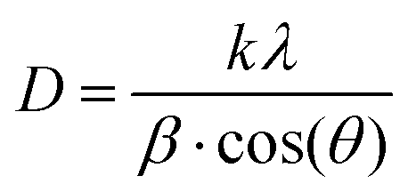
Fig. 1 shows the XRD patterns of nickel oxide thin films produced on glass and Si substrates at different oxygen flow rates. Nickel oxide deposited on glass surfaces displays a Ni2O3(002) peak [PDF#14-0481] and two peaks corresponding to NiO (111) and NiO (200) [PDF#47-1049], as seen in Fig. 1a.14–16 Conversely, nickel oxide deposited on Si substrates displays similar peaks in addition to a Ni2O3 (202) peak (refer to Fig. 1b). In an oxygen-rich environment, nickel oxide thin films exist in both the Ni2O3 and NiO phases. The XRD results indicate significant differences in the phase composition of nickel oxide films that were deposited on glass compared to that of those deposited on Si substrates. On glass substrates, the Ni2O3 phase dominates, especially with increased oxygen flow rates (sample N-35). On Si substrates, the NiO phase exists at oxygen/argon ratios under 30%, whereas the Ni2O3 phase dominates at higher ratios.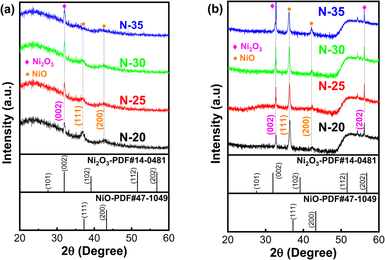 | ||
| Fig. 1 X-ray diffraction (XRD) patterns of nickel oxide thin films at varying oxygen flow rates, grown on (a) glass substrate and (b) n-Si substrate. | ||
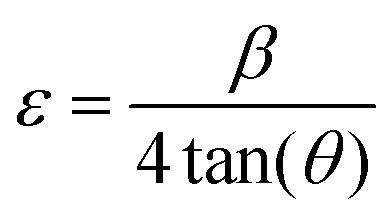
The average crystallite size (D) of nanoscale materials can be calculated using Scherrer's equation.17,18
 | (1) |
 and
and  , where D is the crystallite size which is regarded as one for minimum dislocation density.17,18 The average crystallite sizes of the nickel oxide thin films grown on the glass substrate, derived from Scherrer equation, were 19.53 nm, 20.35 nm, 21.63 nm and 18.12 nm for N-20, N-25, N-30 and N-35, respectively. Evidently, as the partial oxygen ratio increases from 20% to 30%, the crystallinity of the nickel oxide thin film enhances. However, a further increase to 35% results in a decline of crystallinity. Conversely, an excessive oxygen amount will lead to the presence of numerous interstitial oxygen atoms in the film. Formation of defects induces diminished film crystallinity. This outcome is analogous to that reported in the previous work.
In addition, the structural mismatch between NiO (cubic structure) and Ni2O3 (hexagonal structure) results in the diffraction peak shifting to a higher angle, which in turn causes stacking faults to occur during the deposition process.19,20 This result shows that in an oxygen-poor environment, the nickel oxide films are deposited with the stoichiometric nickel oxide (NiO) or the Ni2+ state predominates in the film structure. In contrast, in an oxygen-rich environment, the numerous Ni3+ ions generated in the nickel oxide crystal lattice will frequently combine with oxygen to form the Ni2O3 phase.12 The creation of Ni3+ ions in the nickel oxide crystal lattice is ascribed to the charge displacement that occurs between two adjacent Ni2+ atoms, which is brought about by vacancies in the Ni atoms. The generation of Ni vacancies will contribute to increasing the concentration of hole carriers, thereby improving the conductivity of the nickel oxide thin film, which will be discussed in the electrical properties section. The structure parameters are shown in Table 1.
| Samples | 2θ (°) | Full width at half maximum (FWHM) (°) | Crystallite size (nm) | Microstrain (×10−3) | Dislocation density (×10−3 nm−2) |
|---|---|---|---|---|---|
| N-20 | 31.97 | 0.42 | 19.53 | 6.44 | 2.62 |
| N-25 | 31.99 | 0.41 | 20.35 | 6.18 | 2.42 |
| N-30 | 32.01 | 0.38 | 21.63 | 5.87 | 2.14 |
| N-35 | 32.01 | 0.46 | 18.12 | 6.94 | 3.05 |
The surface morphology and grain sizes of nickel oxide thin films deposited on a glass substrate were analyzed using SEM and the line-cut method, as seen in Fig. 2. On the film surface, the particles assume a relatively uniform shape. Despite the increase in the oxygen flow rate, the grain size (approximately 20 nm) and micro-strain were unaffected. Instead, it demonstrates a clearly stronger impact on the ratio of Ni3+ to Ni2+. Consequently, the electrical and optical properties were also influenced, which will be discussed in sections to come. Moreover, as the flow of oxygen gas increases, the thickness of the nickel oxide film tends to decrease, probably as a result of the interaction between nickel and oxygen gas.21,22 The outcome is oxidation and a growth of deficiencies within the nickel lattice, resulting in the formation of a NiOx lattice rather than an ideal NiO lattice.23
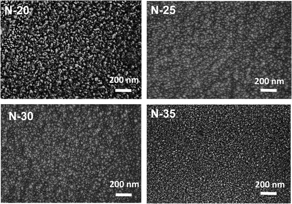 | ||
| Fig. 2 SEM images of nickel oxide thin films deposited on the glass substrate with different oxygen flow rates. | ||
The elemental compositions and ionic states of nickel oxide films with different amounts of inlet oxygen were investigated using X-ray photoelectron spectroscopy (XPS), as shown in Fig. 3. The Ni 2p3/2 core in the energy range from 859 eV to 866 eV and the Ni 2p1/2 core in the energy range from 867 eV to 880 eV are represented by distinct spectral peaks in Fig. 3(a). Furthermore, the unique spectral peak of the core O 1s in the binding energy range from 527 to 533 eV can be observed in Fig. 3(b). The Ni 2p3/2 peak and the O 1s peak shift slightly to higher energy values when the oxygen content increases from 20% to 35%.24 The peak shift of the Ni 2p3/2 and O 1s cores shows how the elevated oxygen ratio during the reactive sputtering process affects the constituents that make up the nickel oxide thin film. Moreover, a shift of about 0.5 eV of the O 1s core of the N35 sample compared with that of sample N20 is probably due to excessive oxygen in the N35 sample. They might absorb water on the surface and generate a small amount of NiOOH. The existence of NiOOH might cause a peak shift.25
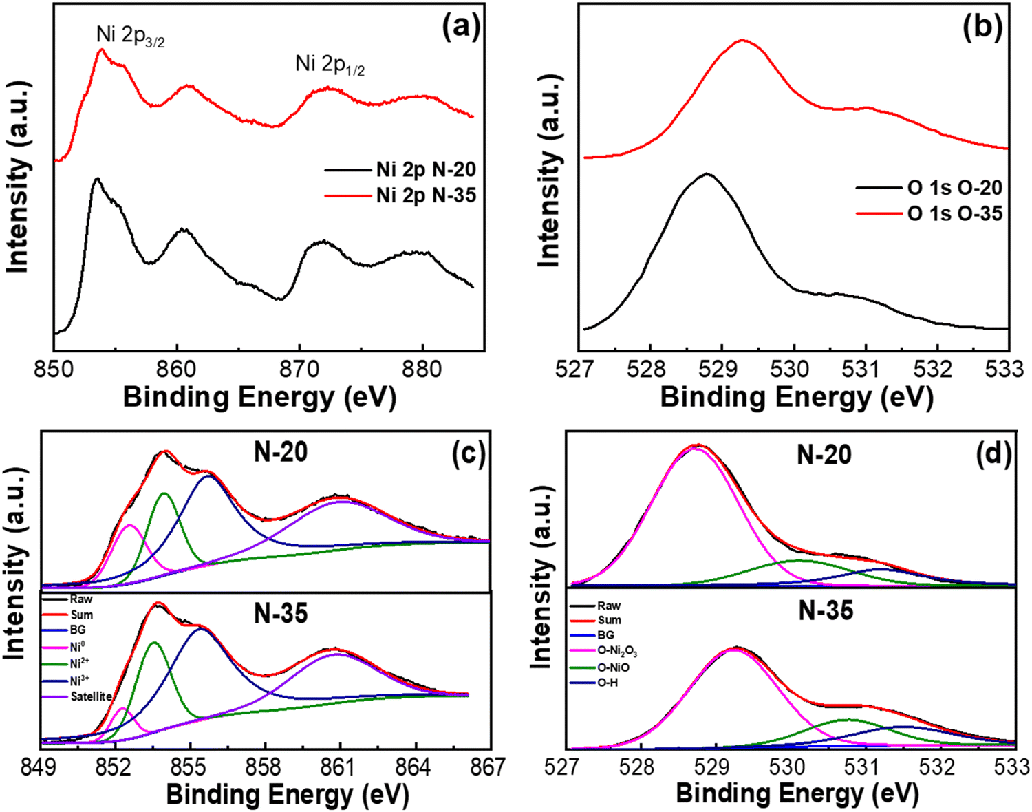 | ||
| Fig. 3 (a) Ni 2p core level, (b) O1s core level, (c) deconvoluted Ni 2p3/2, and (d) deconvoluted O 1s spectra. | ||
Deconvoluting the Ni 2p3/2 core (Fig. 3(c)) and the O1s core (Fig. 3(d)) spectra will allow the focused examination of the ionic states contained in the nickel oxide thin film. There are peaks in the Ni 2p3/2 deconvolution spectrum around 855 eV, which suggest the presence of the Ni3+ state. Furthermore, the existence of the Ni2O3 phase is revealed in the reflected O1s spectrum by a peak at 529 eV. The O1s peak at 530 eV and the Ni 2p3/2 peaks, corresponding to the Ni2+ state, at 853 eV are for the nickel oxide (NiO) phase.20,26,27 For all nickel oxide films, the Ni0 peak is detected at 852 eV, whereas the satellite peaks are observed in the energy range of 861–862 eV (Ni 2p3/2).28 Based on the area ratios of the Ni3+ peak (42.07%, 49.31%) and the Ni2+ peak (19.19%, 15.90%), the oxygen percentages are 20% and 35%. The area percentage of the Ni3+ peak increases from 42.07% to 49.31%, and the Ni2+ peak decreases from 19.19% to 15.90% as the oxygen percentage increases from 20% to 35%. As the amount of oxygen increases, so does the ratio of Ni3+ to Ni2+ states. The proportion of the Ni3+ state in all nickel oxide thin films is significantly higher than that of the Ni2+ state, which is consistent with previous research.29
In an oxygen-rich environment, a thin film of nickel oxide mainly occurs as Ni2O3. The Ni2O3 phase predominates, because of the presence of many Ni3+ cations, which form color centers and give the thin film a dark brown color.26 The XPS results are consistent with the findings from the XRD analysis.
The transmittance of nickel oxide thin films grown under different oxygen flow conditions is demonstrated in Fig. 4. In the visible light spectrum, the relative average transmittance of the N-25, N-30, and N-35 samples is around 50% and tends to decrease as the percentage of oxygen increases. In addition, the absorption edge of the nickel oxide film presents a significant change. Specifically, when the oxygen ratio increases from 20 to 35%, the absorption edge shifts towards the short-wavelength region. The transmittance of the nickel oxide film in the UV region is comparatively high owing to the chemical balance of the film, with excess oxygen and hydrogen possibly existing in the form of –OH.30 This result is consistent with earlier studies showing that being deposited in an oxygen-rich environment reduces the transparency of nickel oxide thin films.31 The low transparency of the nickel oxide films in the visible light range is attributed to the existence of Ni3+ cations in the crystal lattice.32 The second reason is that the transmittance of the thin film is lowered by the additional oxygen, which functions as scattering centers for incident light.
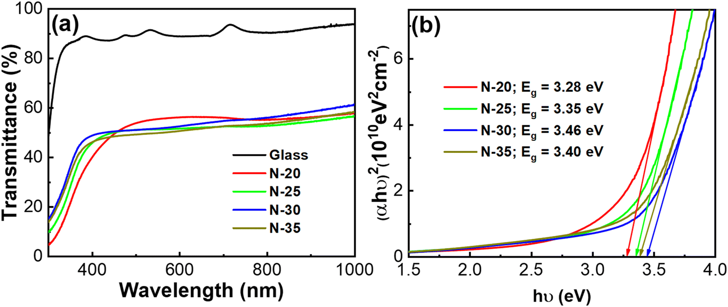 | ||
| Fig. 4 Transmittance spectrum (a) and Tauc plot (b) of nickel oxide thin films deposited under different oxygen gas conditions. | ||
The bandgaps of nickel oxide thin films were determined from the Tauc plots: hν = A(hν − Eg)n, which were derived from the absorption spectrum.32 The relationship between the square of (αhν) and the photon energy (hν) for crystalline nickel oxide thin films growing at various oxygen gas flow rates is illustrated in the inset of Fig. 4. It was found that nickel oxide thin films in an oxygen-excessive environment have optical bandgap energies of roughly 3.4 eV. Specifically, 3.28 eV, 3.35 eV, 3.46 eV, and 3.40 eV correspond to oxygen ratios of 20%, 25%, 30%, and 35%. Our nickel oxide thin films have a higher optical bandgap value than that of F. G. El Desouky.33 This indicates that the optical bandgap is widened by the simultaneous presence of two phases, NiO and Ni2O3. Furthermore, higher oxygen ratios lead to higher carrier concentrations. Therefore, according to the Burstein–Moss effect, wider optical bandgaps come as a result of these degenerated semiconducting thin films.34 However, if the oxygen ratio reaches above 35%, various defects will exist in the films. In addition, the defect density around grain boundaries is typically significantly greater than that within the grain. Smaller grain boundary results in reduced defect density. These defects frequently serve as charge trap centers so the optical bandgap energies tend to decrease.35,36
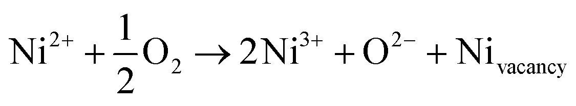
The electrical properties of the nickel oxide thin films, including Hall mobility (μH), carrier concentration (nH), and resistivity (ρ), under various oxygen flow conditions, are presented in Fig. 5 and Table 2. The resistivity values are 0.65, 0.44, 0.28 and 0.43 Ω cm, corresponding to oxygen percentages of 20%, 25%, 30%, and 35%, respectively. The carrier mobility increases gradually from 0.43 cm2 V−1 s−1 to 0.61 cm2 V−1 s−1, when the oxygen level increases from 20% to 30% and then decreases to 0.20 cm2 V−1 s−1 at an oxygen ratio of 35%. The carrier concentration increases from 2.23 × 1019 cm−3 to 7.46 × 1019 cm−3. These values are considerably higher than those reported in a previous study.37 This can be attributed to the oxidation of one Ni2+ ion into two Ni3+ ions and a Ni vacancy in an oxygen-rich environment. The higher the oxygen inlet is, the more Ni3+ ions and free carriers are generated. This oxidation helps to maintain the electroneutral state of the nickel oxide thin film, as described in eqn (2).28 However, for sample N-35, a great amount of defects reduce hole mobility due to defect scattering, leading to an increase in the resistivity of the film.
 | (2) |
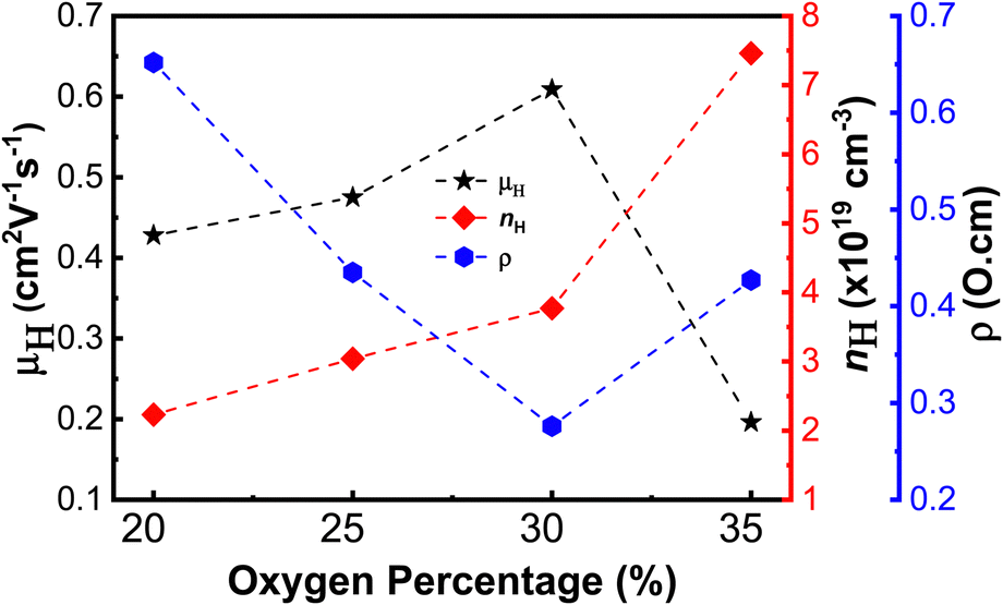 | ||
| Fig. 5 The Hall mobility (μH), carrier concentration (nH), and resistivity (ρ) versus the function of oxygen percentage of nickel oxide thin films. | ||
| Sample | Optical properties | Electrical properties | |||
|---|---|---|---|---|---|
| Transmittance (400–800 nm) (%) | E g (eV) | Mobility (cm2 V−1 s−1) | Carrier concentration (×1019 cm−3) | Resistivity (Ω cm) | |
| N-20 | 56 | 3.28 | 0.43 | 2.23 | 0.65 |
| N-25 | 52 | 3.35 | 0.48 | 3.04 | 0.44 |
| N-30 | 51 | 3.46 | 0.61 | 3.77 | 0.28 |
| N-35 | 50 | 3.40 | 0.20 | 7.46 | 0.43 |
The current density–voltage (J–V) characteristics of the p–n heterojunctions between the n-Si substrate and nickel oxide (oxygen ratios of 20% and 30%) are shown in Fig. 6. The nickel oxide thin film has successfully established a p–n heterojunction on the n-type Si substrate, as evidenced by the typical characteristic diode curves obtained. The J–V curves can be characterized using the thermoionic emission model shown in the following equation:38,39
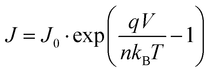 | (3) |
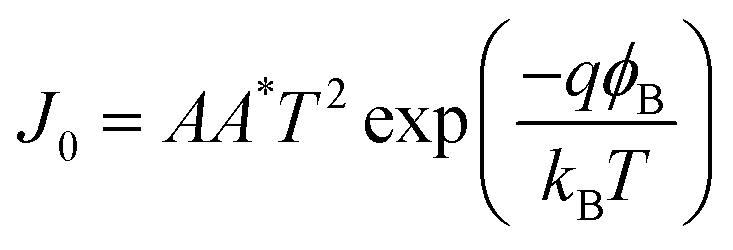 | (4) |
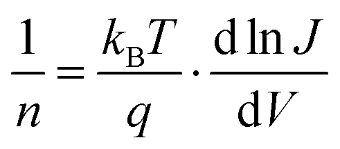 | (5) |
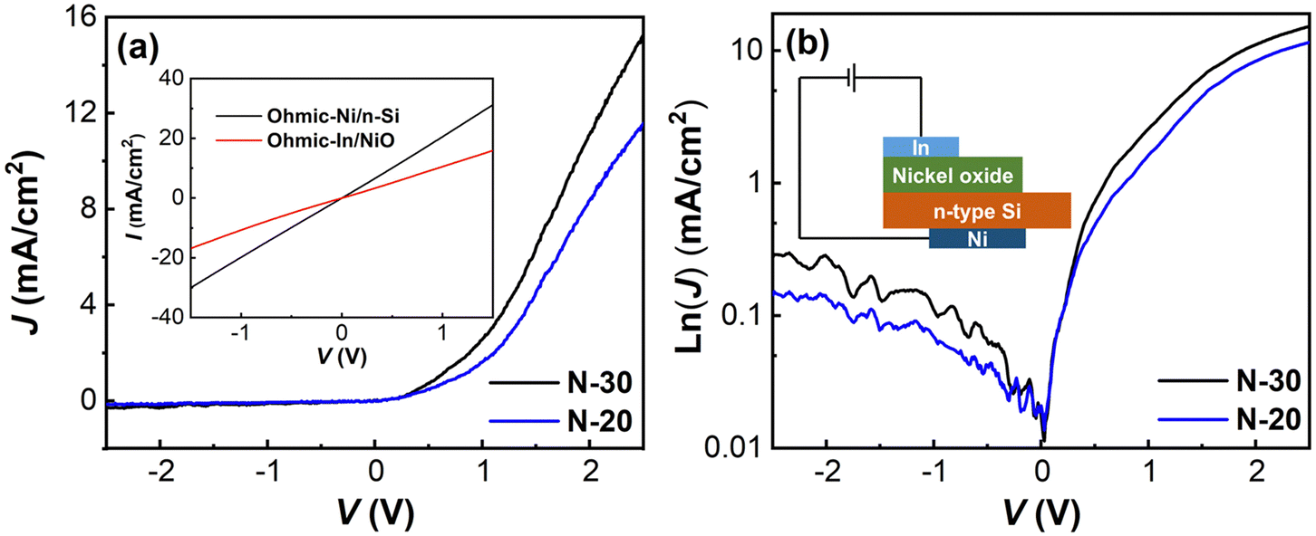 | ||
| Fig. 6 Linear (a) and semi-logarithmic (b) J–V characteristics of the nickel oxide/n-Si diode. Inset of (a): I–V characteristics of Ni/n-Si and In/NiO. | ||
| Sample | V turn-on (V) | Ideality factor – n | Effective barrier heights – ΦB (eV) | Rectification ratio (±2 V) | R S (Ω) | Saturation current density (A cm−2) |
|---|---|---|---|---|---|---|
| N-20 | 0.91 | 9.62 | 0.71 | 64 | 230.79 | 1.66 × 10⁻⁶ |
| N-30 | 0.78 | 6.86 | 0.72 | 68 | 150.99 | 1.12 × 10⁻⁶ |
4. Conclusion
In summary, nickel oxide films were successfully reactively sputter deposited on glass and silicon substrates. When the partial oxygen ratio increases from 20% to 35%, analysis results indicate a phase transition from NiO to Ni2O3 corresponding to the transition of Ni2+ to Ni3+, an increase in the Ni vacancy sites and enhancement of the hole concentration. As Ni vacancy density increased, the crystal size of the film decreased. This led to reduced carrier mobility and decreased film transmittance. The results show that at a 30% oxygen ratio, the nickel oxide thin films present the best electrical and optical properties with a transmittance of 51%, a bandgap energy of 3.46 eV, a carrier concentration of 3.77 × 1019 cm−3, a mobility of 0.61 cm2 V−1 s−1, and a resistivity of 0.28 Ω cm. In addition, the I–V curves of Ni2O3/n-Si heterojunctions demonstrated that the best diode parameters (VOC = 0.78 V, n = 6.86, and ΦB = 0.72 eV) can be achieved at an oxygen percentage of 30%. The results demonstrate the potential of nickel oxide films for future electronic applications such as wide bandgap photodiodes.Data availability
The data used to support the findings of this study are available from the corresponding author upon request.Conflicts of interest
The authors have no conflicts to disclose.Acknowledgements
This work belongs to the project T2025 funded by Ho Chi Minh City University of Technology and Education, Ho Chi Minh City, Vietnam.References
- C. Mrabet, M. Ben Amor, A. Boukhachem, M. Amlouk and T. Manoubi, Ceram. Int., 2016, 42, 5963–5978 CrossRef CAS.
- Y. Gong, S. Zhang, H. Gao, Z. Ma, S. Hu and Z. Tan, Sustainable Energy Fuels, 2020, 4, 4415–4458 RSC.
- B. G. S. González, G. Vescio, J. L. Frieiro, J. López-Vidrier, S. Hernández and A. Cirera, Adv. Mater. Interfaces, 2023, 10, 2300035 CrossRef.
- M. Mishra, S. Barthwal, B. R. Tak and R. Singh, Phys. Status Solidi A, 2021, 218, 2100241 CrossRef CAS.
- J. D. Hwang and M. C. Lin, Sens. Actuators, A, 2023, 349, 114087 CrossRef CAS.
- M. G. G. C. S. Chou, C. M. Hsiung, C. P. Wang and R. Y. Yang, Int. J. Photoenergy, 2010, 2010, 9 CrossRef.
- M. Matsumiya, F. Qiu, W. Shin, N. Izu, N. Murayama and S. Kanzaki, Thin Solid Films, 2002, 419, 213–217 CrossRef CAS.
- W. L. Jang, Y. M. Lu, W. S. Hwang, T. L. Hsiung and H. P. Wang, Appl. Phys. Lett., 2009, 94, 10–13 Search PubMed.
- P. Salunkhe, M. A. Muhammed and D. Kekuda, Appl. Phys. A: Mater. Sci. Process., 2021, 127, 1–12 CrossRef.
- K. Jouini, A. Raouafi, W. Dridi, M. Daoudi, B. Mustapha, R. Chtourou and F. Hosni, Optik, 2019, 195, 163109 CrossRef CAS.
- F. A. F. Lahiji, S. Bairagi, R. Magnusson, M. A. Sortica, D. Primetzhofer, E. Ekström, B. Paul, A. le Febvrier and P. Eklund, J. Vac. Sci. Technol., A, 2023, 41, 063402 CrossRef.
- S. Nandy, U. N. Maiti, C. K. Ghosh and K. K. Chattopadhyay, J. Phys.: Condens. Matter, 2009, 21, 115804 CrossRef CAS PubMed.
- M. C. Li, M. J. Dai, S. S. Lin, S. C. Chen, J. Xu, X. L. Liu, E. H. Wu, A. N. Ding, J. H. Gong and H. Sun, Ceram. Int., 2022, 48, 2820–2825 CrossRef CAS.
- H. Wu, L. Wang, Y. Wang, S. Guo and Z. Shen, J. Alloys Compd., 2012, 525, 82–86 CrossRef CAS.
- N. M. Vuong, T. N. Trung, T. T. Hien, N. D. Chinh, N. D. Quang, D. Lee, D. Kim, T. L. Phan and D. Kim, Mater. Trans., 2015, 56, 1354–1357 CrossRef.
- N. K. Binh, P. N. Y. Nhi, T. B. Quan, P. M. Tam, N. N. Phuong, D. M. Tuan, P. T. K. Hang and P. H. Phuong, J. Vac. Sci. Technol., B, 2024, 42, 062205 CrossRef CAS.
- H. D. Ngo, V. D. T. Truong, V. Q. Le, H. P. Pham and T. K. H. Pham, Beilstein J. Nanotechnol., 2024, 15, 253–1259 Search PubMed.
- M. S. Jamal, S. A. Shahahmadi, P. Chelvanathan, H. F. Alharbi, M. R. Karim, M. Ahmad Dar, M. Luqman, N. H. Alharthi, Y. S. Al-Harthi, M. Aminuzzaman, N. Asim, K. Sopian, S. K. Tiong, N. Amin and M. Akhtaruzzaman, Results Phys., 2019, 14, 102360 CrossRef.
- H. L. Chen, Y. M. Lu and W. S. Hwang, Mater. Trans., 2005, 46, 872–879 CrossRef CAS.
- M. Aftab, M. Z. Butt, D. Ali, M. U. Tanveer and A. Hussnain, Proc. Pakistan Acad. Sci. Part A, 2020, 57, 51–74 Search PubMed.
- P. Gao, L. J. Meng, M. P. Dos Santos, V. Teixeira and M. Andritschky, Vacuum, 2000, 56, 143–148 CrossRef CAS.
- G. Gottardi, N. Laidani, V. Micheli, R. Bartali and M. Anderle, Surf. Coat. Technol., 2008, 202, 2332–2337 CrossRef CAS.
- A. H. Hammad, M. S. Abdel-wahab, S. Vattamkandathil and A. R. Ansari, Phys. B, 2019, 568, 6–12 CrossRef CAS.
- S. Uhlenbrock, C. Scharfschwerdt, M. Neumann, G. Illing and H. J. Freund, J. Phys.: Condens. Matter, 1992, 4, 7973–7978 CrossRef CAS.
- K. Xu, L. Wang, C. Ge, L. Wang, B. Wang, Z. Wang, C. Zhang and G. Liu, Energy Environ. Mater., 2024, 7, 1–11 Search PubMed.
- B. Sasi and K. G. Gopchandran, Nanotechnology, 2007, 18, 115613 CrossRef.
- A. M. Elseman, L. Luo and Q. L. Song, Dalton Trans., 2020, 49, 14243–14250 RSC.
- H. Kim, K. Kim and J. Hong, Coatings, 2023, 13, 1954 CrossRef CAS.
- S. Nandy, B. Saha, M. K. Mitra and K. K. Chattopadhyay, J. Mater. Sci., 2007, 42, 5766–5772 CrossRef CAS.
- H. Liu, W. Zheng, X. Yan and B. Feng, J. Alloys Compd., 2008, 462, 356–361 CrossRef CAS.
- A. H. Hammad, M. S. Abdel-wahab, S. Vattamkandathil and A. R. Ansari, Phys. B, 2019, 568, 6–12 CrossRef CAS.
- F. Şenaslan, M. Taşdemir and A. Çelik, Appl. Phys. A: Mater. Sci. Process., 2021, 127, 1–9 CrossRef.
- F. G. El Desouky, H. A. Saleh and D. Atta, Phys. Scr., 2024, 99, 75905 CrossRef CAS.
- Z. M. Gibbs, A. Lalonde and G. J. Snyder, New J. Phys., 2013, 15, 075020 CrossRef CAS.
- M. Kumar, Mater. Res. Express, 2019, 6, 096404 CrossRef CAS.
- A. M. Reddy, C. W. Byun, S. K. Joo, A. S. Reddy and P. S. Reddy, Electron. Mater. Lett., 2014, 10, 887–892 CrossRef CAS.
- P. Salunkhe, A. V. Muhammed Ali and D. Kekuda, Mater. Res. Express, 2020, 7, 016427 CrossRef CAS.
- S. Kaya, Appl. Phys. A: Mater. Sci. Process., 2020, 126, 1–9 CrossRef.
- H. P. Pham, T. H. Y. Nguyen, A. H.-T. Nguyen, N. T. Vo, T. G. Le Thuy, H. H. Nguyen, H. T. M. Hoa and Q. T. Tran, J. Photochem. Photobiol. A Chem., 2019, 388, 112157 CrossRef.
- J. M. Shah, Y. L. Li, T. Gessmann and E. F. Schubert, J. Appl. Phys., 2003, 94, 2627–2630 CrossRef CAS.
- M. Yilmaz, H. Kacus, M. L. Grilli and S. Aydogan, J. Sandwich Struct. Mater., 2021, 23, 1383–1402 CrossRef CAS.
| This journal is © The Royal Society of Chemistry 2025 |