DOI:
10.1039/D4MA01163E
(Paper)
Mater. Adv., 2025,
6, 1119-1130
Influence of alkali metal ions on the defect induced photoluminescence properties of double tungstate compounds ACe(WO4)2 (A = Li, Na, K): experimental and ab initio theoretical study†
Received
26th November 2024
, Accepted 6th January 2025
First published on 13th January 2025
Abstract
Defect-induced alkali-metal cerium double tungstate compounds, ACe(WO4)2 (where A = Li, Na, K), have been synthesized through a trisodium citrate-based hydrothermal process. The influence of alkali-metal ions on the local structure of ACe(WO4)2 has been explored using various methods, including the Rietveld technique for powder X-ray diffraction (XRD), scanning electron microscopy (SEM), and transmission electron microscopy (TEM). Although the ACe(WO4)2 compounds exhibit similar transitions, they differ in luminescent intensity. Notably, in the case of the alkali metal Na, the material displays a larger crystal compactness due to its comparable ionic radii with Ce3+. This proximity indicates lower distortion. Conversely, Li and K possess significantly different ionic radii from Ce3+, leading to pronounced crystal distortion. The ACe(WO4)2 materials show emissions in blue and green spectra, including blue I (439 nm), blue II (462 nm), blue III (487 nm), and green (531 nm). The blue I emission is attributed to the 5d → 4f transition within the CeO8 polyhedra, whereas the blue III emission arises from the same transition within CeO7 polyhedra. The blue II and green emissions result from the formation of CeO6 polyhedra. Additionally, ab initio calculations employing density functional theory reveal that the valence and conduction bands are composed of O 2p and O 2p–Ce 5d hybridization, respectively. Notably, the 5dxy, 5dxz, 5dyz, 5dx2−y2, and 5dxz, 5dx2−y2 orbitals significantly contribute to the 5d–4f transition within CeO7 and CeO6 polyhedra, respectively. The resulting Commission Internationale de l'Éclairage (CIE) coordinates in the blue region, coupled with a correlated color temperature (CCT) of approximately 7800 K, suggest that ACe(WO4)2 materials hold promise for applications in cold solid-state lighting.
1. Introduction
Double tungstate compounds have garnered significant attention due to their intriguing optical and electronic properties, making them promising candidates for various technological applications.1–4 In recent years, there has been significant interest in rare earth-based double tungstate scheelite materials due to their unique optical characteristics, such as high luminescence quantum efficiency, narrow line width and excellent thermal stability.5–7 These materials exhibit UV absorption and emit visible light, making them well-suited for applications like phosphorescent materials, luminescent diodes and optical fibres etc.8,9 Among these compounds, ACe(WO4)2 (where A = Li, Na, K) has emerged as a subject of intense research, owing to its unique defect-induced photoluminescence properties. The incorporation of alkali metal ions (Li+, Na+, K+) into the crystal lattice of ACe(WO4)2 introduces defects that lead to distinct optical characteristics, opening new avenues for the design of advanced optoelectronic devices. Understanding this impact is vital for tailoring optical properties to specific applications. A recent study by Shimemura et al. focused on ACe(WO4)2 materials, where A represents Li+, Na+, and K+. While they investigated the emission properties, detailed photoluminescence information was lacking.10 In another report, Shimemura et al. discussed LiCe(WO4)2 as a fluorescent material, considering combined luminescence of Ce3+ and WO4.2–11 The photoluminescence properties of materials have gained prominence due to their applications in various fields, ranging from lighting and displays to sensors and lasers. ACe(WO4)2 compounds, with their intriguing luminescent behavior, offer a versatile platform for tailoring and optimizing photoluminescence emissions. These emissions are primarily attributed to the interaction between 4f and 5d electron orbitals of Ce3+ ions within the crystal lattice. The manipulation of these emissions through controlled defect engineering, particularly the introduction of oxygen vacancies (VO), provides an innovative approach to enhance the luminescence efficiency and tune the emission colors.
In this context, the present study delves into the intricate relationship between alkali metal ions, defect-induced photoluminescence, and crystal structure in ACe(WO4)2 compounds. By systematically investigating the impact of Li+, Na+, and K+ ions on the defect formation and subsequent photoluminescence properties, valuable insights can be gained into the underlying mechanisms governing these phenomena. Through a combination of experimental characterization techniques and advanced theoretical modeling, a comprehensive understanding of the defect-induced photoluminescence behavior in ACe(WO4)2 compounds can be achieved. The insights garnered from this research not only contribute to the fundamental understanding of defect engineering in double tungstate materials but also pave the way for the development of novel optoelectronic devices with tailored luminescent properties.
This article presents the hydrothermal synthesis of scheelite-type LiCe(WO4)2, NaCe(WO4)2 and KCe(WO4)2 using tri-sodium citrate as an organic additive. It examines the impact of alkali metal ions on crystal structure distortion and optical properties of ACe(WO4)2 (A = Li, Na, K). As per literature, there is no report on ab initio band structures of ACe(WO4)2 clusters are employed to elucidate photoluminescence properties. This study provides insights into electronic and optical properties of ACe(WO4)2 and informs the development of new materials with tailored optical attributes.
2. Experimental section
2.1 Materials and synthesis
Scheelite-type ACe(WO4)2 (A = Li, Na, K) materials were synthesized using a conventional hydrothermal method. To prepare Li/Na/KCe(WO4)2, 0.17 mmol (0.074 g) of cerium nitrate [Ce(NO3)3·6H2O, Merck, Germany, 98.5% purity] and 0.17 mmol (0.044 g) of trisodium citrate dihydrate (Na3Cit·2H2O, Sigma Aldrich, ≥99.0% purity) were dissolved in 60 mL of deionized (DI) water at room temperature. Another 20 mL of an aqueous solution containing 0.34 mmol (0.089 g) of lithium tungstate (Li2WO4·H2O, Merck, Germany, 99.0% purity) or 0.112 g of sodium tungstate (Na2WO4·H2O, Merck, Germany, ≥99.0% purity) or 0.111 g of potassium tungstate (K2WO4·2H2O, Merck, Germany, 99.0% purity) was added dropwise over 30 minutes with continuous magnetic stirring, maintaining the pH of the reaction medium at 7. The initially transparent solution turned milky white. Subsequently, the solution was transferred into a Teflon autoclave and maintained at 180 °C for 24 hours. After cooling to room temperature, the resulting product was collected via centrifugation and subsequently washed with DI water and ethanol. The washed product was then dried at 70 °C for 10 hours, followed by calcination at 800 °C for 5 hours to obtain the powdered final product. Thus, materials with different alkali metal sources (Li, Na, K) were synthesized, and the resulting samples were designated as LCWO, NCWO, and KCWO respectively.
2.2 Measurement and characterization
Various analytical techniques were employed to investigate the properties of the material. X-ray diffraction (XRD) was utilized to extract structural and microstructural refinement parameters via the least-squares method. The Rigaku Ultima III powder diffractometer from Japan, equipped with CuKα radiation (λ = 1.5404 Å), was employed for recording XRD patterns. The experimental profiles were fitted using the most appropriate pseudo-Voigt analytical function, accounting for asymmetry. A fourth-order polynomial function was applied to fit the background of each pattern. The sample morphology was examined using a field emission scanning electron microscope (FESEM; Hitachi S-4800) operating at 5 kV. Raman spectra were analyzed using the Alpha 300 instrument from Wintec, with a 530 nm laser (3 mW output and a 2 m spot size). Infrared spectra, ranging from 400 to 4000 cm−1, were recorded using the IR Prestige. X-ray photoelectron spectra (XPS) were collected through the PHI Versa Probe III Scanning XPS Microprobe with Al K source. UV-vis absorption spectra were measured using a UV-vis spectrophotometer (V-630, JASCO). Photoluminescence emission spectra were obtained using an FP-8300, JASCO, equipped with a 100 W Xe lamp, and measurements were conducted at room temperature. The outcomes derived from these techniques hold the potential to optimize material synthesis and customize properties to suit specific applications.
2.3
Ab initio density functional theory
To compute the spin-polarized electronic band structure, projected density of states (PDOS), and total density of states (TDOS) for multiple atoms, the VASP simulation software was employed utilizing the plane-wave pseudopotential (PAW) method. The basis set utilized was the Perdew–Burke–Ernzerhof (PBE) exchange correlation ultra-soft potentials.12,13 The considered atoms included Li (1s2 2s1), Na (1s2 2s2 2p6 3s1), K (3s2 3p6 4s1), Ce (5s2 5p6 4f1 5d1 6s2), W (5p6 6s2 5d10), and O (2s2 2p4). The supercell structure with the lowest single-point ground state energy was optimized using a 4 × 4 × 4 Monkhorst–Pack k-point grid. Subsequently, the band structure was calculated along symmetry points Γ → X → H1 → C → H → Y → Γ → C. A plane wave cutoff energy of 520 eV was chosen, and convergence energy was achieved within the range of 220 to 620 eV. To ensure accuracy, maximum atomic displacement and stress were constrained at 5 × 10⁻⁴ Å and 0.02 GPa, respectively. Each atom was subjected to a 0.01 eV Hellmann–Feynman force. For precise computational convergence, the EDIFF and force EDIFG parameters were set to 10−6 eV and 10−3 eV, respectively. This information aids in comprehending atomic behavior within diverse materials and can guide the design of materials possessing specific electronic properties.
3. Result and discussion
3.1 Phase and crystal structure analyses of the samples by XRD, FESEM, TEM
The obtained X-ray diffraction (XRD) patterns of ACe(WO4)2 materials are presented in Fig. 1(a–c). These patterns closely resemble those of the triclinic scheelite-type material (ICSD card: 200520, space group: P![[1 with combining macron]](https://www.rsc.org/images/entities/char_0031_0304.gif) (2)).14 The absence of additional peaks verifies the phase purity of the samples and a strong agreement between observed and calculated XRD patterns via Rietveld refinement is evident. The refinement process was pursued until Rp, Rwp, Rexp, and χ2 converged within acceptable ranges.15 Detailed structural refinement information is available in Tables S1 and S2 of the ESI.† The refinement reveals that W, Ce, and A atoms form a cage-like structure connected by O atoms. Ce atoms establish regular CeO8 polyhedra, A atoms form AO4 tetrahedra, and W atoms create WO6 octahedra with 8, 4, and 6 coordinated O atoms, respectively. Each AO4 shares an edge with WO6 octahedra and links to CeO8 polyhedra through O atoms. Schematic representations of the triclinic unit cell of ACWO are depicted in Fig. 1(d)–(f). Rietveld analyses additionally indicate that W atoms possess inversion symmetry, resulting in edge-sharing octahedra forming W4O16 as a tetramer via W2O2 bridged O atoms. The lattice parameters, unit cell volume, A–O, Ce–O, and W–O bond lengths, as well as A–O–W, Ce–O–W, and O–Ce–O bond angles, decrease in LCWO and KCWO compared to NCWO unit cells, indicating distortion of the unit cells. This trend can be attributed to the ionic radius of Na+ (r = 0.99 Å, CN = 4), which is closest to that of Ce3+ (r = 1.14 Å, CN = 8), compared to the ionic radius of Li+ (r = 0.59 Å, CN = 4) and K+ (r = 1.37 Å, CN = 4). As a result, the crystal compactness is most significant in NCWO while both LCWO and KCWO show abnormal lattice distortion. The lower lattice parameters observed in LCWO and KCWO compared to NCWO can be attributed to the distinct ionic sizes and coordination number mismatches resulting from the substitution of Ce3+ with Li+ and K+.16,17 The significantly smaller ionic radius of Li+ induces a compression of the lattice as it attempts to accommodate the smaller ions, leading to reduced lattice parameters in LCWO. Conversely, the larger ionic radius of K+ results in lattice distortion due to spacing mismatches, contributing to a decrease in lattice parameters in KCWO. These combined effects, arising from differences in ionic radii and coordination numbers, lead to lattice distortions and a subsequent decrease in lattice parameters in both LCWO and KCWO compared to NCWO.
(2)).14 The absence of additional peaks verifies the phase purity of the samples and a strong agreement between observed and calculated XRD patterns via Rietveld refinement is evident. The refinement process was pursued until Rp, Rwp, Rexp, and χ2 converged within acceptable ranges.15 Detailed structural refinement information is available in Tables S1 and S2 of the ESI.† The refinement reveals that W, Ce, and A atoms form a cage-like structure connected by O atoms. Ce atoms establish regular CeO8 polyhedra, A atoms form AO4 tetrahedra, and W atoms create WO6 octahedra with 8, 4, and 6 coordinated O atoms, respectively. Each AO4 shares an edge with WO6 octahedra and links to CeO8 polyhedra through O atoms. Schematic representations of the triclinic unit cell of ACWO are depicted in Fig. 1(d)–(f). Rietveld analyses additionally indicate that W atoms possess inversion symmetry, resulting in edge-sharing octahedra forming W4O16 as a tetramer via W2O2 bridged O atoms. The lattice parameters, unit cell volume, A–O, Ce–O, and W–O bond lengths, as well as A–O–W, Ce–O–W, and O–Ce–O bond angles, decrease in LCWO and KCWO compared to NCWO unit cells, indicating distortion of the unit cells. This trend can be attributed to the ionic radius of Na+ (r = 0.99 Å, CN = 4), which is closest to that of Ce3+ (r = 1.14 Å, CN = 8), compared to the ionic radius of Li+ (r = 0.59 Å, CN = 4) and K+ (r = 1.37 Å, CN = 4). As a result, the crystal compactness is most significant in NCWO while both LCWO and KCWO show abnormal lattice distortion. The lower lattice parameters observed in LCWO and KCWO compared to NCWO can be attributed to the distinct ionic sizes and coordination number mismatches resulting from the substitution of Ce3+ with Li+ and K+.16,17 The significantly smaller ionic radius of Li+ induces a compression of the lattice as it attempts to accommodate the smaller ions, leading to reduced lattice parameters in LCWO. Conversely, the larger ionic radius of K+ results in lattice distortion due to spacing mismatches, contributing to a decrease in lattice parameters in KCWO. These combined effects, arising from differences in ionic radii and coordination numbers, lead to lattice distortions and a subsequent decrease in lattice parameters in both LCWO and KCWO compared to NCWO.
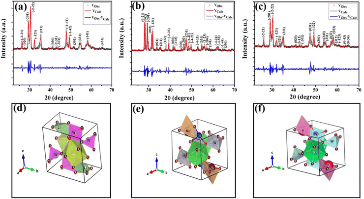 |
| | Fig. 1 XRD patterns (a)–(c) and triclinic unit cell's structure (d)–(f) of LCWO, NCWO, KCWO respectively. | |
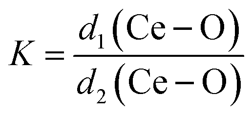
The degree of CeO8 polyhedron distortion (K) is quantified as ∼1.066, 1.046, and 1.082 for LCWO, NCWO, and KCWO using the relation  , where d1(Ce–O) and d2(Ce–O) represent different bond lengths. Similarly, WO6 octahedron distortion (N) is assessed as ∼1.132, 1.095, and 1.285 using the relation
  , where α1(O–W–O) and α2(O–W–O) denote distinct bond angles, affirming greater VO-induced distortion in LCWO and KCWO compared to NCWO.18 Furthermore, a reduction in the c/a ratio in NCWO relative to LCWO and KCWO indicates the influence of dipole–dipole interactions on short-range disorder attributed to charge entrapment at the VO site.19
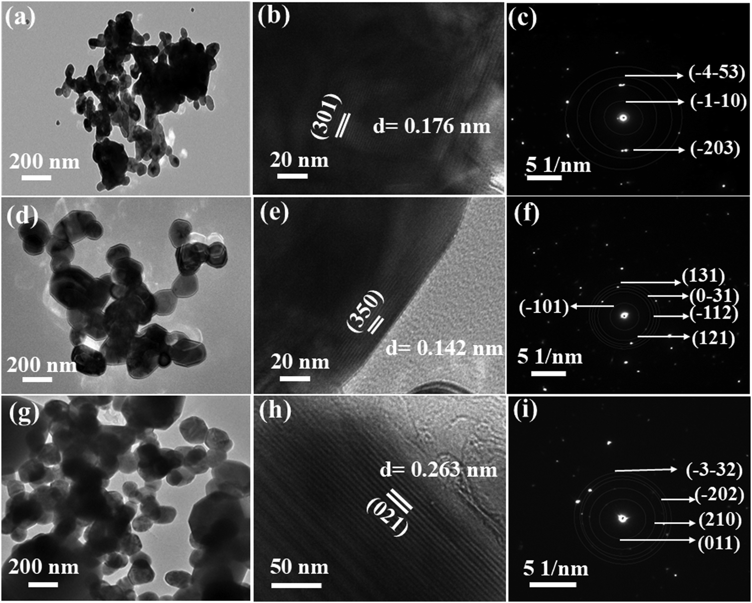
The field emission scanning electron microscopy (FESEM) analysis demonstrates notable morphological variations among the ACWO samples, depicted in Fig. 2(a–c). LCWO exhibits an irregular shape, whereas a truncated octahedral morphology is observed in NCWO and KCWO. This structure becomes more pronounced in NCWO, attributed to enhanced crystal compactness. These findings highlight the pivotal role of alkali metal ions in modulating the morphology during the hydrothermal synthesis process. To gain more insights into the precise shape and size of the particles, further analysis was conducted using transmission electron microscopy (TEM). Upon TEM examination, the samples exhibited irregular to truncated octahedral shapes and sizes (Fig. 3(a), (d) and (g)) for LCWO, NCWO, and KCWO, respectively. High-resolution TEM (HRTEM) images allowed for the determination of d-spacing values, which were found to be 0.176 nm for LCWO, 0.142 nm for NCWO, and 0.263 nm for KCWO (Fig. 3(b), (e), and (h)). These d-spacing values correspond to the (301), (350), and (021) planes of LCWO, NCWO, and KCWO, respectively. Notably, these results are consistent with the X-ray diffraction (XRD) data presented in Fig. 1(a–c). Fig. 3(c), (f), and (i) illustrate the selected area electron diffraction (SAED) patterns of LCWO, NCWO, and KCWO samples, respectively, derived from the TEM images. The diffraction spots represented by white points in these patterns correspond to specific crystal planes. Importantly, these diffraction spots (Fig. 3(c), (f) and (i)) align well with the XRD data shown in Fig. 1(a–c). The HRTEM images along with their corresponding d-spacing measurements support the crystallographic properties of LCWO, NCWO, and KCWO samples. These observations validate the structural characteristics of the materials under investigation.
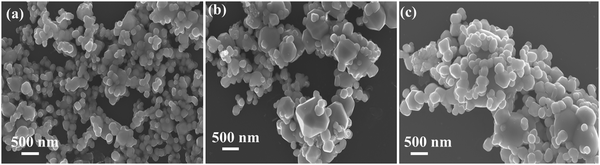 |
| | Fig. 2 (a)–(c) FESEM image of LCWO, NCWO, KCWO respectively. | |
 |
| | Fig. 3 TEM image, HRTEM image and corresponding SAED pattern of LCWO (a)–(c), NCWO (d)–(f), KCWO (g)–(i) respectively. | |
3.2 Investigations of defects in ACWO nanostructures by FTIR, Raman and X-ray photoelectron spectroscopies
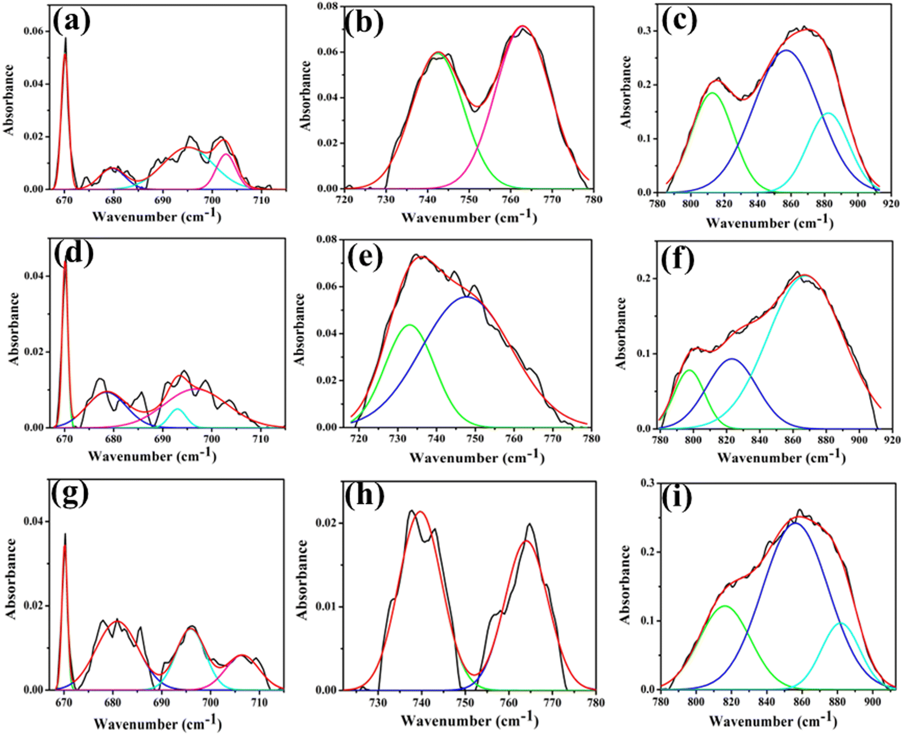
FTIR and Raman spectra serve as analytical techniques to assess structural distortions in terms of vibrational frequencies. In the context of materials like ACWO, these techniques offer insights into crystal structure and the presence of defects, such as vacancies (VO). The FTIR spectrum of ACWO manifests four absorption bands (Fig. S1, ESI†), corresponding to internal vibrations of the WO6 octahedron. Within the WRO6 structure, tungsten ions occupy the centre of regular octahedra formed by six oxygen ions with 2i site symmetry. Group theory dictates that the symmetry modes can be expressed as ΓOh= 36 Au.
The emergence of an oxygen vacancy within the lattice can lead to a distorted octahedral structure, specifically the WDO6 octahedron. This introduces a reduction in lattice symmetry, subsequently affecting the vibrational frequencies of the system. The detailed deconvolution of FTIR bands is provided in the ESI† (Table S3). Deconvolution of two bands (780–920 and 673–715 cm−1) in the FTIR spectra reveals the peaks at 679, 693, 697, 797, 823, 868 cm−1 for NCWO. Peaks at 697 and 868 cm−1 correspond to the stretching vibration (→ O → W → O →) of WDO6 and WRO6 octahedra respectively. Other deconvoluted peaks align with the asymmetric stretching of two-oxygen bridged W2O2 in WRO6 and WDO6 octahedra.20,21 This blue shift in the FTIR spectrum of LCWO and KCWO signifies defects introduced into the crystal lattice, leading to alterations in the local chemical environment of atoms or molecules within the material. The peaks at 733 and 748 cm−1 for NCWO, correspond to W–O bending vibration of WDO6 and WRO6 respectively (Fig. 4). Similarly, a blue shift is also observed for LCWO and KCWO.22,23 However, that peak shifting alone may not be sufficient to fully characterize a material's defects. Weighted percentage calculation from area under the curves indicates WDO6 ∼44%, 30%, and 48% for LCWO, NCWO, and KCWO respectively. A noticeable blue shift is observed in LCWO and KCWO, indicating more pronounced VO in those samples than in NCWO. The WDO6/WRO6 ratios stand at 0.785, 0.428, and 0.923 for LCWO, NCWO, and KCWO respectively, indicating greater octahedral distortion in LCWO and KCWO compared to NCWO.
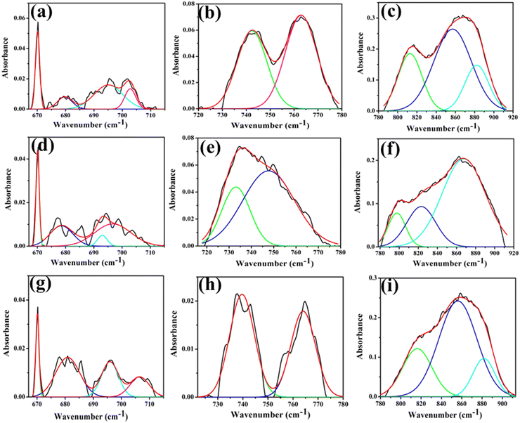 |
| | Fig. 4 (a) Deconvoluted curves of the FTIR bands 660–717, 718–777 and 778–910 cm−1 of LCWO (a)–(c), NCWO (d)–(f) and KCWO (g)–(i) respectively. | |
The Raman spectrum of NCWO exhibits peaks at 338, 389, 463, and 534 cm−1, aligning with the vibrational motion of WO6 octahedra and W2O2 units (Fig. 5). The peak at 463 cm−1 is attributed to the Ag symmetric stretching mode of the W2O2 unit. The remaining peaks correspond to asymmetric and symmetric bending vibrations of O–W–O within the Ag mode, along with the asymmetric stretching mode of the W2O2 unit.24,25 Furthermore, the relatively lower intensity of Raman peaks observed in KCWO and LCWO compared to NCWO can be attributed to symmetry disruption caused by an increased presence of oxygen vacancies and antisite defects.26 The other peaks at 680, 786, 930 cm−1 are due to secondary scattering.
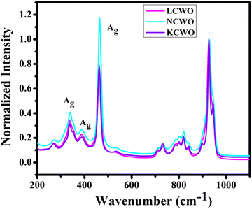 |
| | Fig. 5 Raman spectra of ACWO nanostructures. | |
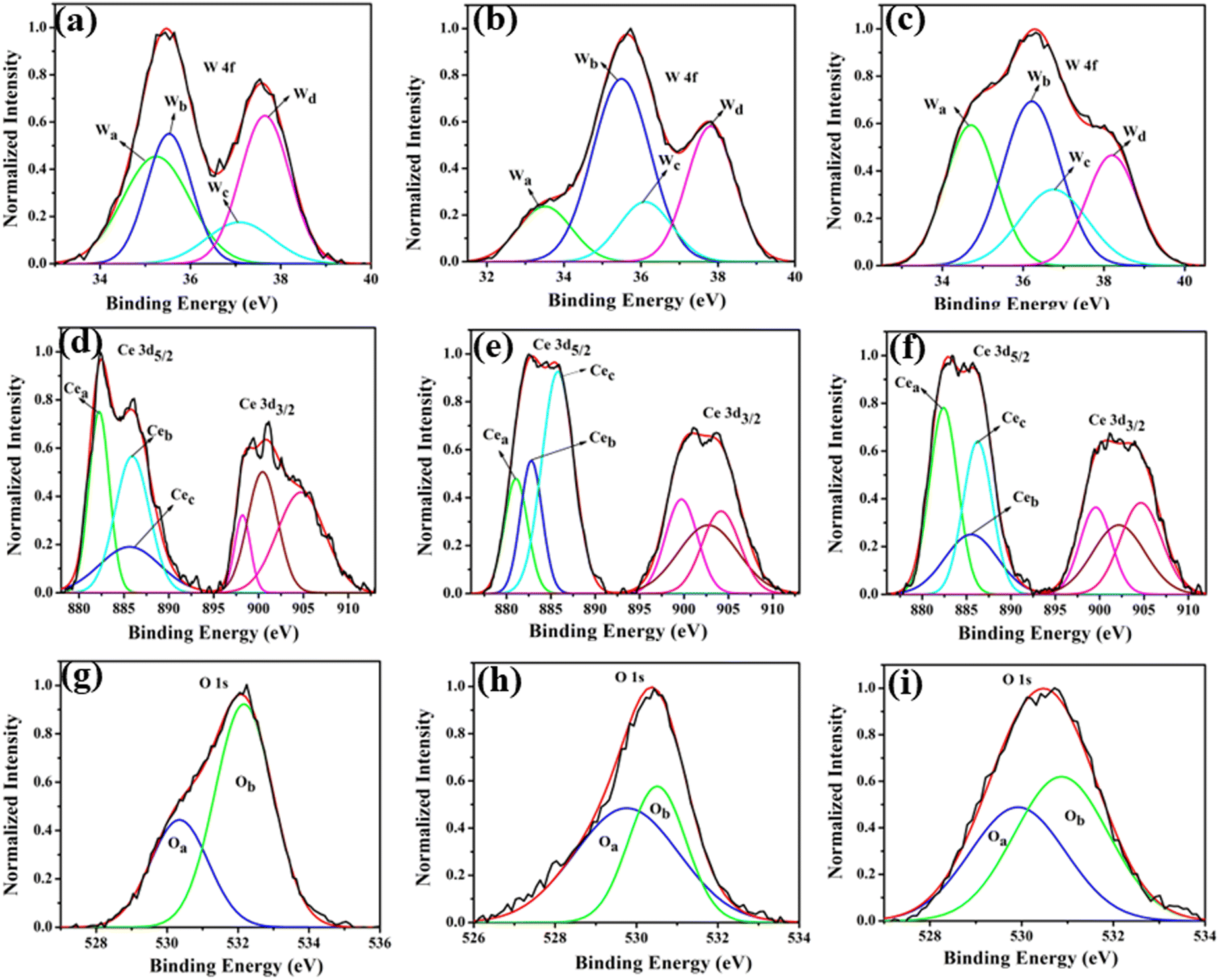
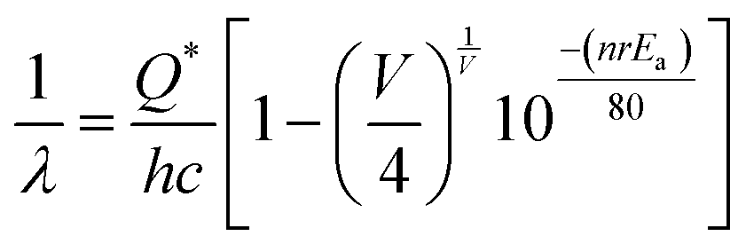
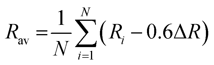
XPS analysis was undertaken to delve into the chemical states of Li, Na, K, Ce, W, and O, aiming to enhance comprehension of VO-induced disorder effects on material electronic structure. The obtained XPS data for all elements were adjusted to account for the C 1s peak attributed to adventitious carbon on the sample surface due to atmospheric exposure.27 This C 1s peak carries a binding energy of 284.6 eV. The survey scan (Fig. S2 of ESI†) encompasses core binding energies of Li, Na, K, Ce, W, and O within the energy range of 0 to 1100 eV. This scan aids in identifying chemical states present in the samples. Further, high-resolution spectra of W, Ce, and O from all samples are illustrated in Fig. 6. These spectra offer detailed insights into the electronic structure of these materials, particularly highlighting changes prompted by the presence of VO-induced disorder.
 |
| | Fig. 6 (a)–(c) XPS W 4f, (d)–(f) XPS Ce 3d, (g)–(i) XPS O 1s core level spectra of LCWO, NCWO, KCWO respectively. | |
Fig. 6(a)–(c) reveal two asymmetric peaks in XPS spectra at 35.4 and 37.4 eV, originating from spin–orbit splitted 4f7/2 and 4f5/2 orbitals of W6+.28–30 Deconvolution of these spectra results in four peaks, Wa, Wb, Wc, and Wd, corresponding to diverse electronic states of W. Wa and Wc associate with WDO6, while Wb and Wd signify WRO6. The electronegativity disparity between W and O suggests an ionic W–O bond. The presence of VO heightens the effective charge on W, inducing electron–electron repulsion and reducing binding energies of the 4f7/2 and 4f5/2 states in WDO6. Estimated WDO6 percentages are higher in LCWO (∼43%) and KCWO (∼45%) compared to NCWO (∼26%), aligning with FTIR findings. In Fig. 6(d)–(f), two asymmetric peaks within the ranges 877–891 eV and 895–910 eV manifest in Ce 3d spectra. Deconvolution of the 3d5/2 peak yields three peaks, Cea, Ceb, and Cec, associated with distinct Ce electronic environments. Cec corresponds to CeO8, while Cea and Ceb relate to CeO7 and CeO6, containing VO and 2VO, respectively. Analysis of Ce spectra demonstrates VO's impact, shortening Ce–O bond lengths and heightening electron–electron repulsion at the Ce site, thereby lowering binding energies of 3d5/2 and 3d3/2 orbitals.31 Scrutinizing the data indicates a reduction in Cea weight percentage in NCWO (∼21%) compared to LCWO (∼34%) and KCWO (∼40%), implying VO suppression in NCWO. XPS analysis of O 1s manifests an asymmetric peak. Deconvolution of this spectrum yields one peak at 530.6 eV, attributed to lattice oxygen within Ce–O–Ce bonds in the crystal structure.32–34 Another peak at 532.4 eV corresponds to chemisorbed oxygen linked to oxygen vacancies. Notably, the area under the peak at 532.4 eV is greater in LCWO and KCWO compared to NCWO, signifying a higher oxygen vacancy amount in those samples than in NCWO.
3.3 Optical properties of the as-prepared ACWO samples by UV-vis, photoluminescence spectroscopy
The UV-vis absorption spectra of ACWO materials reveal an optical band gap of approximately 3.10 eV for LCWO, 3.14 eV for NCWO, and 3.06 eV for KCWO (depicted in Fig. S3, ESI†). The valence band (VB) of ACWO consists of O 2p–W 5d hybridization, while the conduction band (CB) of ACWO comprises W-5d, Ce-4f, and a minor contribution of O-2p, as indicated by a DFT-based ab initio calculation (discussed later).35 A broad peak at 380 nm is observed in the photoluminescence excitation (PLE) spectra for ACWO samples when monitored at an emission wavelength of 531 nm (Fig. S4, ESI†). The 380 nm peak in the PLE spectra is attributed to charge transfer (CT) absorption within WO6 octahedra. This absorption process involves electronic charge transfer between different atomic species, specifically between O-2p and W-5d within the WO6 octahedra. Furthermore, the emission spectra recorded in the visible region with an excitation wavelength of 380 nm are illustrated in Fig. 7(a)–(c). The emission spectra in the visible region upon excitation at 380 nm likely correspond to the relaxation of excited states formed during the CT absorption process. The luminescence characteristics of the samples reveal four peaks in the visible region upon excitation at 380 nm. A prominent peak is observed at 439 nm (blue I, 22![[thin space (1/6-em)]](https://www.rsc.org/images/entities/char_2009.gif) 779 cm−1), followed by two peaks in the blue region at 462 nm (blue II, 21645 cm−1) and 487 nm (blue III, 20533 cm−1), along with a green emission at 531 nm (green, 18832 cm−1). Previous studies have proposed that emissions from scheelite materials are largely due to 5d to 4f transitions within rare earth elements. However, the precise mechanism remains debated due to factors such as crystal field, polarizability, etc., significantly affecting emission characteristics.36
779 cm−1), followed by two peaks in the blue region at 462 nm (blue II, 21645 cm−1) and 487 nm (blue III, 20533 cm−1), along with a green emission at 531 nm (green, 18832 cm−1). Previous studies have proposed that emissions from scheelite materials are largely due to 5d to 4f transitions within rare earth elements. However, the precise mechanism remains debated due to factors such as crystal field, polarizability, etc., significantly affecting emission characteristics.36
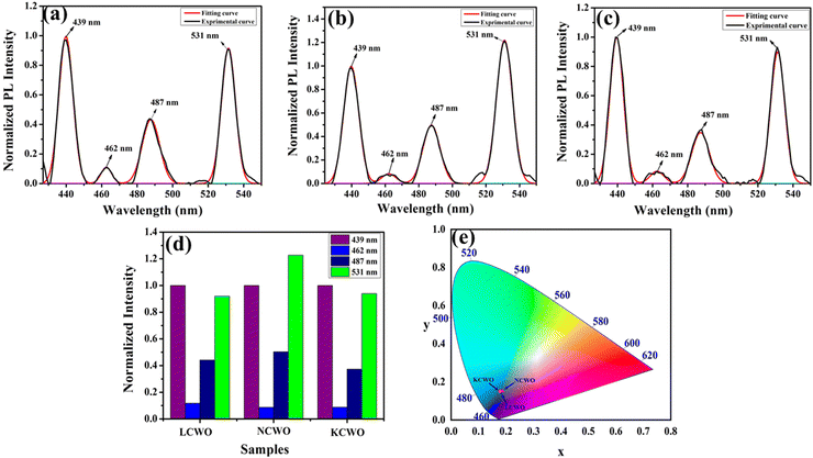 |
| | Fig. 7 Photoluminescence spectra of (a) LCWO, (b) NCWO and (c) KCWO respectively. (d) Normalized PL intensity ratio of emission wavelengths (e) The CIE chromaticity diagram of the ACWO. | |
To comprehend the emission wavelength (λ) based on the 5d–4f transition of Ce3+ within a regular CeO8 polyhedron, we have employed a relationship provided by van Uitert et al.:37
| | 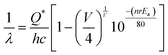 | (1) |
where,
Q* represents the energy of 5d band edge of free Ce
3+ ion (= 50
000 cm
−1), V is the valence of the Ce
3+, ‘
n’ is the number of anions in the immediate shell around Ce
3+,
Ea is electron affinity of the atoms forming anions and ‘
r’ is defined as the difference between average bond length and radius of anion of CeO
8 polyhedra (1.03 Å). We have calculated wavelength ∼437 nm is highly corroborating with our experimental blue I emission at 439 nm. By using
eqn (1) with CeO
7 and CeO
6 configurations, it was calculated that the emission wavelengths for these configurations are approximately 470 nm and 522 nm, respectively. These values match well with the experimentally observed blue III and green emissions (as shown in
Fig. 7). It is believed that V
O defects alter the energy of the 5d orbitals of Ce
3+ in CeO
7 and CeO
6, resulting in different emissions. To further understand this, the crystal field stabilization energy and centroid shift of the d-orbitals (
εc(1, 3+, A)) of Ce
3+ in different CeO
8 polyhedra were calculated using Dorenbos's
eqn (2) and (3):
38| | | εcfs(1, 3+, A) = βRav−2 | (2) |
| | | εc(1, 3+, A) = 6.35 − EC(1, 3+, A) eV | (3) |
where,
β = 1.35 × 10⁹ pm
2 cm
−1 for Ce
3+ and
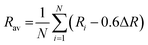
;
Ri denotes bond lengths to the
N coordinating anions in distorted lattice.
The calculated values of εc(1, 3+, Ce3+) for CeO8, CeO7, and CeO6 are approximately 5.94, 5.66, and 5.41 eV for LCWO, 5.93, 5.69, and 5.46 eV for NCWO, and 5.92, 5.62, and 5.35 eV for KCWO, respectively. Furthermore, the values of εcfs(1, 3+, Ce3+) are in the order of 2.06, 3.44, and 4.69 eV for LCWO, 2.01, 3.30, and 4.42 eV for NCWO, and 2.16, 3.62, and 4.99 eV for KCWO, respectively. It was also determined that the difference between the 5D0–2F5/2 and 5D0–2F7/2 transitions is sapproximately 2000 cm−1. The emissions labelled as “blue I” and “blue II” exhibit a distinct energy difference of around 1134 cm−1. This disparity suggests that these emissions have different energy levels, indicating that the “blue II” emission cannot be attributed to the 5D0–2F7/2 transition within CeO8 polyhedra or a 5d orbital split transition. This implies that the origin of the “blue II” emission differs from these known transitions. The presence of two distinct εc(1, 3+, Ce3+) states within CeO6 units are associated with the existence of two vacancy oxygen (VO) defects (discussed later in DFT calculation). An intriguing finding is that the centroid shift εc(1, 3+, Ce3+) value of CeO7 and CeO6 is observed to decrease, indicating presence of more oxygen vacancies in KCWO and LCWO compared to NCWO. This suggests that VO defects significantly influence the values of εcfs and εc, consequently determining the emission wavelength (λ) for the 5d–4f transition within CeO7 and CeO6.
The formation of VO and 2VO defects can be comprehended through the Kröger–Vink notation, which delineates the relationship between defects and stoichiometry in ionic crystals. Electrons are released into the host matrix, leading to the creation of ionized defect states  and
and  which can be represented by eqn 4(a) and 4(b):
| | 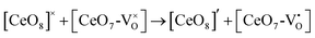 | (4a) |
| | 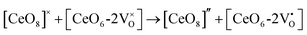 | (4b) |
where [CeO
8]′ and [CeO
8]′′ denote electron donors and

and

are the electron acceptors those exhibit blue III and green emission.
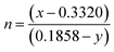
Additionally, the luminescent intensity demonstrates variations with the presence of Li+, Na+, and K+ ions. Specifically, NCWO exhibits the strongest intensity for blue III and green emissions, whereas LCWO and KCWO display relatively weaker intensity for these emissions. It is suggested that the presence of A+ ions affects the lattice parameters, thereby influencing the crystal field that surrounds the rare earth ions.39 In our study, it is evident that the alkali metal ions do not alter the shape and peak position of the photoluminescence (PL) spectra; rather, they solely affect the luminescence intensity. It has been previously confirmed that NCWO exhibits reduced lattice distortion compared to LCWO and KCWO. This reduction in lattice distortion is associated with an increase in luminescence intensity in NCWO compared to both LCWO and KCWO.40,41 We have also checked the stability of the materials in terms of fluorescent spectra taken over a duration of 7 days, one month, and two months (Fig. S5, ESI†). The estimated Commission Internationale de l'Eclairage (CIE) coordinates are (0.179, 0.148), (0.181, 0.149), and (0.178, 0.148) for LCWO, NCWO, and KCWO, respectively, indicating a blue emission (Fig. 7(e)).42,43 However, the variations in the coordinates are attributed to different contributions from blue II and III emissions. According to eqn (5), the color purity is calculated to be approximately 91% for all samples.
| |  | (5) |
where (
x,
y) represents the color coordinates of the phosphor; (
xi,
yi) is the illuminant point of the 1931 CIE Standard Source with the colour coordinates of (0.3101, 0.3162); (
xd,
yd) refers to colour coordinates of the dominant wavelength and the correlated colour temperatures (CCTs) have been calculated from McCamy's relation as given in
eqn (6),
44 and it was found that (CCTs) ∼ 7763, 7803 and 7784 K for LCWO, NCWO and KCWO respectively.
| | | CCT = 449n3 + 3525n2 + 6823.3n + 5520.3 | (6) |
where
and (
x,
y) represents the chromaticity co-ordinates. Hence, it may be stated that ACWO materials are excellent for blue lightening.
3.4 Density functional theory (DFT) calculation of ACWO
In our study, ab initio density functional theory was employed to investigate the electronic properties and optical emissions induced by vacancies (VO, 2VO) in ACWO materials. We performed calculations on the electronic band structure, total density of states (TDOS), and angular momentum projected partial densities of states (PDOS) for both pure ACWO and structurally distorted ACWO models containing VO and 2VO. These models were created by removing oxygen atoms to mimic the CeO7 (VO) and CeO6 (2VO) structures. Through optimization of the ACWO unit cell, we determined lattice parameters and bond lengths consistent with experimental results, providing confidence in the accuracy of our calculations. To begin, we set the top of the valence band maxima (VBM) to zero in all calculations. ACWO exhibited behavior as an indirect band material, with energy gaps (Eg) approximately 3.19 eV, 3.14 eV, and 3.15 eV for LCWO, NCWO, and KCWO, respectively, at the Γ- and X-points (depicted in Fig. 8(a), 9(a), and 10(a)). While the conduction band minimum (CBM) showed spin polarization, the valence band maximum (VBM) remained spin-unpolarized. These calculated band gap values closely matched experimental values, attesting to the accuracy of our calculations (as illustrated in Fig. S3, ESI†). The pronounced curvature at CBM implied a low effective electron mass, suggesting high electron mobility within ACWO and a longer mean free path for electrons. Conversely, the curvature at VBM was comparatively low, indicating a higher effective hole mass.
 |
| | Fig. 8 (a) Band structure and (b) spin polarised TDOS and PDOS of (c) Li, (d) Ce, (e) W and (f) O of pristine-LCWO. | |
 |
| | Fig. 9 (a) Band structure and (b) spin polarised TDOS and PDOS of (c) Na, (d) Ce, (e) W and (f) O of pristine-NCWO. | |
 |
| | Fig. 10 (a) Band structure and (b) spin polarised TDOS and PDOS of (c) K, (d) Ce, (e) W and (f) O of pristine-KCWO. | |
By analyzing the PDOS of A, Ce, W, and O atoms (depicted in Fig. 8(b–f), 9(b–f), and 10(b–f)), we determined that the upper portion of the valence band is predominantly influenced by O-2px, 2py, and 2pz orbitals, with additional contributions from W-2px, 2py, and 2pz orbitals, resulting in minimal curvature. The lower part of the valence band was primarily hybridized with W-5dxz, 5dxy, 5dyz, 5dz2, and O-2px, 2py, and 2pz orbitals. Contributions from Li-2s, Na-3s, K-4s, and Ce-4f orbitals were absent in ACWO samples for valence band formation. Within the CBM, spin-up Ce-4fz3, 4fzx2, 4fxz2, and 4fx3 orbitals were dominant in LCWO, while spin-down Ce-4fz3, 4fzx2, 4fxz2, and 4fx3 orbitals were prevalent in NCWO and KCWO samples. These orbitals were hybridized with O-2px, 2py, and 2pz orbitals, resulting in heightened curvature within the conduction band. The upper layer of the CB was composed of W-4dxy, 4dxz, and 4dz2 orbitals. Based on our findings, we concluded that the valence band is mainly constructed by WO6 octahedra, while both CeO8 polyhedra and WO6 octahedra contribute to the conduction band in ACWO materials. This insight led us to affirm that the band-to-band optical transitions occur through a Ce ↔ O charge transfer process.
The band structures, total densities of states (TDOS), and angular momentum projected partial densities of states (PDOS) for ACWO samples induced by  and
and  , denoted as
  and
and  , have been depicted in Fig. (S6–S8, ESI†) and Fig. (S9–S11, ESI†), respectively. In these figures, it is evident that the valence band maximum (VBM) of
  remains unaltered at the Γ-point, while that of
  shifts to the X-point. Similarly, the conduction band minimum (CBM) remains constant at the Γ-point for
  , whereas it shifts along the Γ–X line for
  . The calculated energy gaps (Eg) for ACWO with
  and
and  are (2.95 and 2.87), (2.99 and 2.97), and (3.00 and 2.96) eV for LCWO, NCWO, and KCWO, respectively. These results are presented in Fig. S6(a), S7(a), and S8(a) (ESI†). The TDOS (Fig. S6(b), S7(b), S8(b), S9(b), S10(b), and S11(b), ESI†) and PDOS (Fig. S6(c)–(f), S7(c)–(f), S8(c)–(f), S9(c)–(f), S10(c)–(f), and S11(c)–(f), ESI†) calculations revealed that the valence bandwidth decreased in
  due to increased localization of O-2p orbitals. This led to an enhanced curvature in both
  and
and  . This behaviour was attributed to an increased overlap between Ce-4fz3, 4fzx2, 4fxz2, 4fx3 and O-2px, 2py, 2pz orbitals, resulting from a reduction in Ce–O bond lengths within CeO8 polyhedra. These modifications have the potential to influence carrier mobility through oxygen vacancies.
Further analysis indicated that  exhibited energy gaps of (2.10, 2.81) eV above VBM,
  displayed energy gaps of (2.14, 2.92) eV above VBM, and
  demonstrated energy gaps of (2.21, 2.94) eV above VBM. In contrast,
  exhibited a defect state at 2.45 eV,
  at 2.31 eV, and
  at 2.38 eV above VBM. Through a meticulous examination of TDOS and PDOS, it was deduced that the Ce-5dxz, 5dx2−y2, 5dxy, and 5dyz orbitals played a pivotal role in the emission properties of ACWO samples containing
  and
and  . A comprehensive list of the orbitals involved in different emissions stemming from diverse deformed structures of CeO8 polyhedra is provided in Table S5 (ESI†) and schematically represented in Fig. 11.
 |
| | Fig. 11 Schematic representation of photoluminescence transitions of ACWO nanomaterial involving different orbitals. | |
4. Conclusions
Pristine ACWO (A = Li, Na, K) clusters were synthesized using a trisodium citrate-assisted hydrothermal method. Notably, as per literature, there is no report on the synthesis procedure for LCWO and KCWO via hydrothermal methods, along with the characterization of their emission properties. These properties reveal pronounced blue I and green emissions, alongside relatively weaker blue II and blue III emissions. Through comprehensive experimental and theoretical investigations, we have demonstrated that all these transitions, occurring within distinct configurations of CeO8 polyhedra, are linked to the Ce 5d → 4f transition. In particular, CeO8 and CeO7 configurations exhibit blue I and blue III emissions, while the CeO6 configuration emits blue II and green colors. This observation suggests that ACWO holds promise as a material suitable for blue light-emitting diodes (LEDs). Our calculations underscore the sensitivity of the O-2p and O-2p–Ce-5d orbitals, which constitute the valence and conduction bands, to defect states. These characteristics can be exploited to finely tune the electrical properties of ACWO. In essence, this research contributes to a deeper comprehension of the optoelectronic traits of pristine ACe(WO4)2 and its oxygen vacancy content. This understanding has implications for the potential applications of ACe(WO4)2, particularly in the domain of optoelectronic devices such as LEDs.
Data availability
All the data will be available on request.
Conflicts of interest
There are no conflicts to declare.
Acknowledgements
One of the authors (NH) thanks Institute of Engineering and Management (IEM), University of Engineering and Management Kolkata, 700160, India, (TM) thanks CSIR, Govt. of India, for financial support during execution of their work. NH and TM have equal contribution to this manuscript.
References
- V. V. Atuchin, V. G. Kesler, N. Y. Maklakova, L. D. Pokrovsky and D. V. Sheglov, Eur. Phys. J. B, 2006, 51, 293–300 CrossRef.
- S. N. Bagaev, V. I. Dashkevich, V. A. Orlovich, S. M. Vatnik, A. A. Pavlyuk and A. M. Yurkin, Quantum Electron., 2011, 41, 189 CrossRef.
- E. V. Alekseev, O. Felbinger, S. Wu, T. Malcherek, W. Depmeier, G. Modolo, T. M. Gesing, S. V. Krivovichev, E. V. Suleimanov, T. A. Gavrilova and L. D. Pokrovsky, J. Solid State Chem., 2013, 204, 59–63 CrossRef.
- C. S. Lim, A. Aleksandrovsky, M. Molokeev, A. Oreshonkov and V. Atuchin, J. Solid State Chem., 2015, 228, 160–166 CrossRef.
- P. Jena, S. K. Gupta, V. Natarajan, M. Sahu, N. Satyanarayana and M. Venkateswarlu, J. Lumin., 2015, 158, 203–210 CrossRef.
- C. H. Chiu, M. F. Wang, C. S. Lee and T. M. Chen, J. Solid State Chem., 2007, 180, 619–627 CrossRef.
- N. Garg, A. K. Mishra, H. K. Poswal, A. K. Tyagi and S. M. Sharma, J. Solid State Chem., 2015, 229, 164–172 CrossRef.
- S. Schwung, D. Rytz, B. Heying, U. C. Rodewald, O. Niehaus, D. Enseling, T. Jüstel and R. Pöttgen, J. Lumin., 2015, 166, 289–294 CrossRef.
- J. R. de Moraes, S. L. Baldochi, L. D. R. L. Soares, V. L. Mazzocchi, C. B. R. Parente and L. C. Courrol, Mater. Res. Bull., 2012, 47, 744–749 CrossRef.
- T. Shimemura, N. Sawaguchi and M. Sasaki, J. Ceram. Soc. Jpn., 2017, 125, 150–154 CrossRef.
- T. Shimemura, N. Sawaguchi and M. Sasaki, J. Ceram. Soc. Jpn., 2016, 124, 938–942 CrossRef.
- L. Ma, Z. Xia, V. Atuchin, M. Molokeev, S. Auluck, A. H. Reshak and Q. Liu, Phys. Chem. Chem. Phys., 2015, 17, 31188–31194 RSC.
- A. H. Reshak, Z. A. Alahmed, J. Bila, V. V. Atuchin, B. G. Bazarov, O. D. Chimitova, M. S. Molokeev, I. P. Prosvirin and A. P. Yelisseyev, J. Phys. Chem. C, 2016, 120, 10559–10568 CrossRef CAS.
- A. K. Munirathnappa, D. Dwibedi, J. Hester, P. Barpanda, D. Swain, C. Narayana and N. G. Sundaram, J. Phys. Chem. C, 2018, 123, 1041–1049 CrossRef.
- W. R. Liu, C. W. Yeh, C. H. Huang, C. C. Lin, Y. C. Chiu, Y. T. Yeh and R. S. Liu, J. Mater. Chem., 2011, 21, 3740–3744 RSC.
- C. S. Lim, A. Aleksandrovsky, M. Molokeev, A. Oreshonkov and V. Atuchin, Molecules, 2021, 26, 7357 CrossRef CAS PubMed.
- C. S. Lim, A. Aleksandrovsky, M. Molokeev, A. Oreshonkov and V. Atuchin, Crystals, 2023, 13, 362 CrossRef CAS.
- G. M. Kuzmicheva, A. V. Eremin, V. B. Rybakov, K. A. Subbotin and E. V. Zharikov, Russ. J. Inorg. Chem., 2009, 54, 854–863 CrossRef.
- L. Li, Y. Su and G. Li, Appl. phys. let, 2007, 90, 054105 CrossRef.
- M. Gancheva, A. Naydenov, R. Iordanova, D. Nihtianova and P. Stefanov, J. Mater. Sci., 2015, 50, 3447–3456 CrossRef.
- A. H. Ahmad and A. K. Arof, Ionics, 2004, 10, 200–205 CrossRef.
- N. Haldar, T. Mondal, T. Das, D. Sarkar, M. Pal and C. K. Ghosh, CrystEngComm, 2023, 25, 3514–3527 RSC.
- N. Haldar, T. Mondal, A. Dutta, D. Sarkar, U. K. Ghorai and C. K. Ghosh, Appl. Phys. A: Mater. Sci. Process., 2023, 129, 708 CrossRef.
- L. Macalik, J. Hanuza and A. A. Kaminskii, J. Mol. Struct., 2000, 555, 289–297 CrossRef.
- A. Jayaraman, S. K. Sharma and S. Y. Wang, J. Raman Spectrosc., 1998, 29, 305–312 CrossRef.
- N. Dirany, E. McRae and M. Arab, CrystEngComm, 2017, 19, 5008–5021 RSC.
- N. Haldar, T. Mondal, T. Das, D. Sarkar, M. Pal and C. K. Ghosh, CrystEngComm, 2023, 25, 3514–3527 RSC.
- V. V. Atuchin, L. D. Pokrovsky, O. Y. Khyzhun, A. K. Sinelnichenko and C. V. Ramana, J. Appl. Phys., 2008, 104, 033518 CrossRef.
- V. V. Atuchin, L. I. Isaenko, V. G. Kesler, Z. S. Lin, M. S. Molokeev, A. P. Yelisseyev and S. A. Zhurkov, J. Solid State Chem., 2012, 187, 159–164 CrossRef.
- O. Y. Khyzhun, V. L. Bekenev, V. V. Atuchin, E. N. Galashov and V. N. Shlegel, Mater. Chem. Phys., 2013, 140, 588–595 CrossRef.
- S. Mandal, C. K. Ghosh, D. Sarkar, U. N. Maiti and K. K. Chattopadhyay, Solid State Sci., 2010, 12, 1803–1808 CrossRef.
- C. V. Ramana, V. V. Atuchin, L. D. Pokrovsky, U. Becker and C. M. Julien, J. Vac. Sci. Technol., A, 2007, 25, 1166–1171 CrossRef CAS.
- C. V. Ramana, R. S. Vemuri, V. V. Kaichev, V. A. Kochubey, A. A. Saraev and V. V. Atuchin, ACS Appl. Mater. Interfaces, 2011, 3, 4370–4373 CrossRef CAS.
- E. J. Rubio, V. V. Atuchin, V. N. Kruchinin, L. D. Pokrovsky, I. P. Prosvirin and C. V. Ramana, J. Phys. Chem. C, 2014, 118, 13644–13651 CrossRef.
- L. S. Cavalcante, F. M. C. Batista, M. A. P. Almeida, A. C. Rabelo, I. C. Nogueira, N. C. Batista, J. A. Varela, M. R. M. C. Santos, E. Longo and M. S. Li, RSC Adv., 2012, 2, 6438–6454 RSC.
- G. Li, Y. Tian, Y. Zhao and J. Lin, Chem. Soc. Rev., 2015, 44, 8688–8713 RSC.
- L. G. Van Uitert, J. Lumin., 1984, 29, 1–9 CrossRef.
- A. Lecointre, A. Bessière, A. J. J. Bos, P. Dorenbos, B. Viana and S. Jacquart, J. Phys. Chem. C, 2011, 115, 4217–4227 CrossRef.
- A. K. Singh, S. K. Singh and S. B. Rai, RSC Adv., 2014, 4, 27039–27061 RSC.
- W. Ran, H. M. Noh, S. H. Park, B. K. Moon, J. H. Jeong, J. H. Kim and J. Shi, Sci. Rep., 2018, 8, 5936 CrossRef PubMed.
- X. Li, Z. Yang, L. Guan, J. Guo, Y. Wang and Q. Guo, J. Alloys Compd., 2009, 478, 684–686 CrossRef.
- N. Haldar, T. Mondal, A. Dutta, D. Sarkar, U. K. Ghorai and C. K. Ghosh, Appl. Phys. A: Mater. Sci. Process., 2023, 129, 708 CrossRef.
- N. Haldar, T. Mondal, T. Das, D. Sarkar, M. Pal, A. H. Seikh and C. K. Ghosh, Mater. Adv, 2024, 5, 4480–4490 RSC.
- M. Rai, G. Kaur, S. K. Singh and S. B. Rai, Dalton Trans., 2015, 44, 6184–6192 RSC.
|
| This journal is © The Royal Society of Chemistry 2025 |
Click here to see how this site uses Cookies. View our privacy policy here. 
 Open Access Article
 This Open Access Article is licensed under a Creative Commons Attribution-Non Commercial 3.0 Unported Licence
 *a and
Tanmoy
Mondal
b
*a and
Tanmoy
Mondal
b

 , where d1(Ce–O) and d2(Ce–O) represent different bond lengths. Similarly, WO6 octahedron distortion (N) is assessed as ∼1.132, 1.095, and 1.285 using the relation
 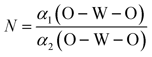 , where α1(O–W–O) and α2(O–W–O) denote distinct bond angles, affirming greater VO-induced distortion in LCWO and KCWO compared to NCWO.18 Furthermore, a reduction in the c/a ratio in NCWO relative to LCWO and KCWO indicates the influence of dipole–dipole interactions on short-range disorder attributed to charge entrapment at the VO site.19


 ; Ri denotes bond lengths to the N coordinating anions in distorted lattice.
 and
and  which can be represented by eqn 4(a) and 4(b):
 and
and  are the electron acceptors those exhibit blue III and green emission.
 and (x, y) represents the chromaticity co-ordinates. Hence, it may be stated that ACWO materials are excellent for blue lightening.


 and
and  , denoted as
  and
and  , have been depicted in Fig. (S6–S8, ESI†) and Fig. (S9–S11, ESI†), respectively. In these figures, it is evident that the valence band maximum (VBM) of
  remains unaltered at the Γ-point, while that of
  shifts to the X-point. Similarly, the conduction band minimum (CBM) remains constant at the Γ-point for
  , whereas it shifts along the Γ–X line for
  . The calculated energy gaps (Eg) for ACWO with
  and
and  are (2.95 and 2.87), (2.99 and 2.97), and (3.00 and 2.96) eV for LCWO, NCWO, and KCWO, respectively. These results are presented in Fig. S6(a), S7(a), and S8(a) (ESI†). The TDOS (Fig. S6(b), S7(b), S8(b), S9(b), S10(b), and S11(b), ESI†) and PDOS (Fig. S6(c)–(f), S7(c)–(f), S8(c)–(f), S9(c)–(f), S10(c)–(f), and S11(c)–(f), ESI†) calculations revealed that the valence bandwidth decreased in
  due to increased localization of O-2p orbitals. This led to an enhanced curvature in both
  and
and  . This behaviour was attributed to an increased overlap between Ce-4fz3, 4fzx2, 4fxz2, 4fx3 and O-2px, 2py, 2pz orbitals, resulting from a reduction in Ce–O bond lengths within CeO8 polyhedra. These modifications have the potential to influence carrier mobility through oxygen vacancies.
 exhibited energy gaps of (2.10, 2.81) eV above VBM,
  displayed energy gaps of (2.14, 2.92) eV above VBM, and
  demonstrated energy gaps of (2.21, 2.94) eV above VBM. In contrast,
  exhibited a defect state at 2.45 eV,
  at 2.31 eV, and
  at 2.38 eV above VBM. Through a meticulous examination of TDOS and PDOS, it was deduced that the Ce-5dxz, 5dx2−y2, 5dxy, and 5dyz orbitals played a pivotal role in the emission properties of ACWO samples containing
  and
and  . A comprehensive list of the orbitals involved in different emissions stemming from diverse deformed structures of CeO8 polyhedra is provided in Table S5 (ESI†) and schematically represented in Fig. 11.