Nanoionics enabled atomic point contact construction and quantum conductance effects
Runsheng
Gao†
ab,
Xiaoyu
Ye†
ab,
Cong
Hu†
ab,
Ziyi
Zhang
abc,
Xinhui
Ji
abc,
Yanyu
Zhang
abc,
Xiaohan
Meng
abd,
Huali
Yang
abc,
Xiaojian
Zhu
 *abc and
Run-Wei
Li
 *abc
*abc
aCAS Key Laboratory of Magnetic Materials and Devices, Ningbo Institute of Materials Technology and Engineering, Chinese Academy of Sciences, Ningbo 315201, China. E-mail: zhuxj@nimte.ac.cn; runweili@nimte.ac.cn
bZhejiang Province Key Laboratory of Magnetic Materials and Application Technology, Ningbo Institute of Materials Technology and Engineering, Chinese Academy of Sciences, Ningbo 315201, China
cCollege of Materials Science and Opto-Electronic Technology, University of Chinese Academy of Sciences, Beijing 100049, China
dSchool of Physical Science and Technology, ShanghaiTech University, Shanghai 201210, China
First published on 18th September 2024
Abstract
The miniaturization of electronic devices is important for the development of high-density and function-integrated information devices. Atomic-point-contact (APC) structures refer to narrow contact areas formed by one or more atoms between two conductive electrodes that produce quantum conductance effects when the electrons pass through the APC channel, providing a new development path for the miniaturization of information devices. Recently, nanoionics has enabled the electric field reconfiguration of APC structures in solid-state electrolytes, offering new approaches to controlling the quantum conductance states, which may lead to the development of emerging information technologies with low power consumption, high speed, and high density. This review provides an overview of APC structures with a focus on the fabrication methods enabled by nanoionics technology. In particular, the advantages of electric field-driven nanoionics in the construction of APC structures are summarized, and the influence of external fields on quantum conductance effects is discussed. Recent studies on electric field regulation of APC structures to achieve precise control of quantum conductance states are also reviewed. The potential applications of quantum conductance effects in memory, computing, and encryption-related information technologies are further explored. Finally, the challenges and future prospects of quantum conductance effects in APC structures are discussed.
Wider impactAtomic point contacts (APCs) represent pivotal structures at the atomic scale, allowing electrons to pass through the quantized energy levels and producing quantum conductance effects. Unlike traditional approaches, nanoionics offers a simple and effective way to build APCs by driving ion migration using localized electric fields. To date, APCs have been successfully developed using various nanoionic materials and have been employed in creating innovative devices, such as resistive switching memories. The quantum conductance of APCs constructed via the nanoionics method features multi-level states and tunable properties, which contribute to developing novel devices with high scalability, fast switching speeds, and low energy consumption.This review provides a comprehensive summary of the advancements in quantum conductance effects within APCs fabricated through the nanoionics technique. It covers the fundamental mechanisms of ion migration, explores the impact of various external fields on quantum effects in APCs, and highlights their significant applications across diverse research areas. Additionally, this review discusses current challenges and offers insights into future development trends. This review will enhance our understanding of quantum conductance effects in APCs and serve as a valuable reference for the design of miniaturized and multifunctional information devices. |
1. Introduction
The rapid growth of artificial intelligence (AI), the Internet of Things (IoT), and autonomous vehicles (AV) has produced massive amounts of data that need to be processed. Over the past few decades, Moore's Law and Dennard's principles have led to the vigorous development of the semiconductor industry. They point out the enhancement of electron and hole mobility within channels and the utilization of high dielectric constant materials to minimize the thickness and size of the devices. Consequently, information devices have undergone continuous miniaturization, scaling down to nanometer sizes.1 However,2 the current technical trajectory of integrated circuit technology is facing significant challenges due to the inherent limitations in indefinitely shrinking the size of physical components.3 Therefore, exploring new technological pathways is essential to advance the miniaturization of information devices and meet future needs such as high-density information storage and high-performance computing.Atomically precise manufacturing, achieved through precise manipulation of atoms and nanostructures, is emerging as a significant approach for advancing manufacturing technologies.4 At this scale, various quantum effects manifest, generating novel physical and chemical properties with potential applications.5 Quantum mechanics determines the fundamental laws governing the behavior of matter and fields at the particle, atomic, and molecular scales. Using the unique quantum effects offers fundamental performance advantages over conventional classical machines.6 In recent years, the fundamental properties of quantum effects, such as quantum coherence, quantum entanglement, and quantum statistics, have been harnessed to conduct plenty of cutting-edge research studies in fields like quantum computing, quantum communication, and quantum precision measurement.7 For instance, a single-atom device with excellent quantum coherence has been constructed.8 This would lead to the emergence of hundreds of high-quality quantum logic qubits within a highly coherent quantum volume, enabling quantum computers to leverage quantum advantages over traditional computers.9 Meanwhile, the quantum conductance effect with many advantages could be produced when the electrons are limited to a narrow constriction, which has a width equal to the electrons' Fermi wavelength and a length much smaller than the mean free path. The conductance is quantized in units of G0, where G0 denotes the conductance quantum (G0 = 2e2/h, where e and h are the electron charge and Planck's constant, respectively). With the continuous advancements in research technology and exploration, quantum conductance phenomena have been observed in nanostructures, such as quantum point contact structures,10,11 metal nanowires,12,13 and graphene,14 at room temperature or even higher. This is in contrast to with two-dimensional electron gas (2DEG) systems, which typically require extremely low temperatures. Experimental results also confirm the precise controllability and multi-level adjustability of quantum conductance states,15 offering diverse options for applications in information storage, computing, and encryption.
Due to the atomic-point-contact (APC) structures operating at the scale of just one or a few atoms, scattering of electrons is minimized as they pass through the APC channel. They serve as an ideal platform for producing and studying quantum conductance effects. Traditionally, APC structures are fabricated using the mechanically controlled break junction (MCBJ) method, which forms the APC structures by separating and reconnecting metal components.16,17 However, this method needs strict operating conditions that limit its practical application. Nanoionics is a research field that centers on the study and application of phenomena associated with the transport of ions in nanoscale materials, focusing on their movement, manipulation, and interactions within these materials. It has diverse applications, including energy storage and conversion systems, sensors, biomedical applications, and information storage systems.18–21 Recent studies indicate that nanoionics-based memory devices, such as resistive switching devices, offer significant advantages including small size, high speed, and low-power operation.22 These benefits help address the scaling limitations of conventional electronic information devices. Consequently, nanoionic devices have garnered renewed interest across various application areas. A key trend in this field is the development of precise ion manipulation techniques aimed at constructing advanced functional nanostructures and exploring new devices with enhanced performance.
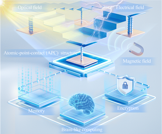
Nanoionics technology has been employed since the 1970s to develop various devices, including electrochemical integral elements and memory storage systems.23 Nanoionics-based APC structures are constructed through electric field-driven ion migration in solid-state electrolytes. The ions are propelled by the external electric field to migrate between the two electrodes, generating the conductive APC structures through redox reactions, which reduce the dominant electron transport scattering mode within the atomic-scale channel.24–26 In 1998, Li et al. fabricated narrow metal-coated copper nanowires via electrochemical deposition of Cu ions, resulting in a narrower structure and the formation of an APC structure, which enabled the emergence of quantized conductance.27 Then, many models were proposed to explain this phenomenon, such as conductive filament, charge trapping defect states, and charge trapping states at metal/oxide interfaces with a change in the Schottky-like barrier.28,29 Terabe et al. developed a silver sulfide/silver/platinum (Ag2S/Ag/Pt) atomic switch device by the scanning tunneling microscopy (STM) method in 2001,30 and then presented a more easily integrated crossbar structure by solid-state electrochemical methods in 2005.15 This device demonstrated highly controllable quantum conductance states compared to those achieved using other methods.31,32 The sandwich structure allows switching operations and quantum conductance states to be controlled by applying voltage to the electrodes, facilitating the study of quantum conductance in APC structures. To date, various APC structures have been fabricated by driving different ions using electric fields.33 These structures have confirmed that the nanoionics method could efficiently realize the quantum conductance effects associated with ballistic electron transport.34 Compared to general techniques, the nanoionics migration offers precise modulation of the APC structures. Additionally, the electric field-driven approach allows for greater diversity in the composition, elements, and structure of APCs, enabling the development of various nanoionic devices for new applications (Fig. 1).35,36 Nanoionics-based devices also exhibit high scalability, fast switching speeds, and low energy consumption.37,38
Herein, this review paper introduces the construction mechanisms and procedures of atomic-point-contact (APC) structures using the electric field-driven ion strategy. It discusses the development and applications of quantum conductance effects within these structures. The advantages of using electric field-driven ions for APC construction are analyzed and summarized. Particularly, the effects of various external physical fields on the optimization and regulation of APC construction and quantum conductance are further discussed. Finally, diverse applications and extensive development prospects for quantum conductance across various fields are also outlined. This review provides valuable insights for the future research, development, and applications of nanoionics-enabled quantum device manufacturing.
2. Traditional construction methods and theory of APC structures
The APC typically refers to a structure where two electrical contacts are connected by a ‘neck’ consisting of several atoms with a width equal to the electrons’ Fermi wavelength. This configuration is often associated with various quantum effects, such as ballistic electron transport, quantum conductance, and thermal conductance quantization.39 The first experimental measurements of the quantum conductance effect in narrow constrictions were conducted in a 2DEG within GaAs–AlGaAs heterostructures (Fig. 2a and b).34,40 Besides this, the quantum conductance effect was also detected when the size of the nanowires was down to the APC structures. As shown in Fig. 2c, when the length of the APC is less than the electron mean free path and its lateral dimension is equal to the Fermi wavelength, the electrons can pass through the point contact by ballistic transportation without colliding and scattering, rather than by diffusive transport, which is typically on a larger scale. Ohnishi et al.41 reported the quantum conductance effect in a metal APC structure, allowing the direct observation of the relationship between electron transport and contact structure. Fig. 2d shows a plot of the conductance change as the tip is withdrawn, indicating that the conductance of the point contact varies with its lateral size in integer multiples of G0. The conductance of a single strand of atoms is 1 G0, while a double strand exhibits twice this conductance. The models of the APC structure for single and double strands of gold atoms are shown in the inset images, corresponding to 1 and 2 G0, respectively. Currently, it can be prepared by several traditional construction methods, such as MCBJ, STM, electrochemical deposition, and photolithography techniques.42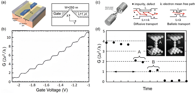 | ||
| Fig. 2 Quantum conductance effect in the APC structures. (a) The illustration diagram of the heterostructure, where a 2DEG-based APC structure is formed at the interface of the heterostructure.34 (b) The relationship between conductance and the gate voltage.40 (c) The schematic diagram of the APC structures and ballistic electron transport.34 (d) The relationship between conductance and the lateral size of the APC structures.41 | ||
2.1. Mechanically controlled break junction technique
The mechanically controlled break-junction (MCBJ) technique has been widely used to construct metallic APC structures and produce the quantum conductance effect. In general, the metallic nanowire with a notch is mechanically broken into two pieces. The two pieces are then brought back into contact by utilizing piezoelectric elements that precisely control the distance. This process results in the formation of a metallic APC structure.43,44 The MCBJ technique has facilitated the discovery of quantized conductance in various metallic wires, including sodium, gold, copper, lead, platinum, aluminium, and niobium (Na, Au, Cu, Pb, Pt, Al, and Nb).45–47 For example, Muller et al. have successfully constructed the Au and Cu metallic APC structures through the MCBJ method. The quantum conductance effect was detected at room temperature, while the conductance of the contacts showed clear plateaus near the integer multiples of G0.48 Strigl et al. also conducted an investigation of the APC structure by stretching Pt nano-bridges fabricated by the MCBJ method (Fig. 3a). The pristine Pt nano-bridge exhibited a conductance of approximately 200 G0 before rupture. The cross-section of the junction was carefully adjusted by stretching the Pt nano-bridge while simultaneously measuring its conductance. As the atomic contact was further elongated, a monoatomic Pt chain was formed once the conductance dropped below 2.5 G0. Using this technique, Pt chains could be consistently created up to seven atoms in length.49 Despite its advantages, precise control of the APC at the atomic scale remains challenging due to piezoelectric element fatigue. Additionally, the integration of the MCBJ method with conventional complementary metal–oxide semiconductor (CMOS) processes and other electronic devices to achieve functionalities such as information storage and computing remains a challenge. These limitations affect the practical applications of the MCBJ method.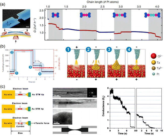 | ||
| Fig. 3 Traditional methods for constructing APC structures. (a) Formation of mono-atomic chains and observation of quantum conductance effects via the MCBJ technique. The schematic shows the experimental setup and an electron micrograph of a suspended Pt nano-bridge (left). The conductance varies with the chain length (right).49 (b) Construction method of APC structures using STM. A Ta metallic APC structure was formed between the STM tip and a 2 nm TaOx layer due to Ta ion diffusion and chemical reactions.11 (c) Schematic diagram of the APC structures constructed through electron irradiation and STM methods (left). The fabrication process of a CNT-clamped Fe nanorod (middle). The conductance changes as a function of time during the formation and thinning of atomic chains at a constant bias of 12 mV (right).50 | ||
2.2. Scanning tunneling microscopy method
Scanning tunneling microscopy (STM) is a widely used scanning probe microscopy technique that provides significantly enhanced resolution compared to other atomic force microscopy techniques. It allows the observation and manipulation of individual atoms with high precision, particularly at low temperatures. In 1990, Eigler et al. demonstrated the manipulation of individual xenon atoms on a single crystal nickel surface using the STM method at a low temperature of 4 K.51 They successfully fabricated rudimentary structures atom by atom, confirming that the APC structure can also be constructed using the STM's atomic manipulation method. By applying a voltage pulse with suitable amplitude and duration between the STM tip and the sample, an electric field with a range from 109 to 1010 V m−1 can be generated. The strong electric field facilitates the extraction of adsorbed atoms from the sample surface, which are then displaced by the STM tip. Furthermore, Terabe et al. proposed an APC structure using nanoionics and solid electrochemical reactions with a STM in an Ag2S/Ag/Pt device.30 When a negative bias is applied to the Pt electrode, Ag ions in Ag2S are reduced to Ag atoms by electrons from the Pt electrode, leading to the deposition of Ag atoms on the surface of Ag2S. These Ag atoms form an atomic bridge that exhibits quantized conductance in units of G0. Applying the reverse bias results in the ionization and dissolution of the Ag atoms in the bridge, causing it to become thinner and eventually break.In addition, Waser et al. constructed a Ta APC structure between the STM tip and a 2 nm amorphous TaOx film (Fig. 3b). Initially, a voltage of 1 V did not cause the rearrangement of atoms. Upon applying a voltage of −3 V, an instantaneous increase in the tunneling current was observed. Subsequently, the current decreased to 104 nA when a −1 mV read voltage was applied. Based on the aforementioned measurement results, the conductance value was calculated to be 1.3 G0. This value exceeds that of a single APC, indicating that both Ta ion migration and electrochemical processes occurred within the TaOx film, forming a Ta metallic APC structure. Ta-based APC structures typically display poor stability due to a high propensity for spontaneous reduction. As a result, the point contact was rendered inoperable after a period of one second.11 Tang et al. employed a combination of electron beam thinning techniques with STM to fabricate the APC structures.50 Carbon nanotubes (CNTs) acted as both nano-connectors and electrodes, forming a CNT-clamped metal atomic chain, including Fe, Co, Ni, and their alloys. The metal nanorods were initially filled into the CNTs, and the surrounding carbon shell was subsequently removed to expose the metal nanorods and make them thin using strong electron irradiation within a transmission electron microscope (TEM). Finally, they successfully fabricated a CNT-clamped metal atomic chain. During the thinning process, the formation of APC structures and quantum conductance effects were observed, as depicted in Fig. 3c. However, STM methods also have several challenges, such as stability which is susceptible to destruction from environmental disturbances. Advanced automation technologies are needed to prepare large-scale and intricate structures with atomic-level precision.
Except for the MCBJ and STM methods, APC structures can also be constructed by electrochemical deposition in a liquid electrolyte. By immersing electrode pairs at a distance of hundreds of nanometers in a metal salt solution, the deposition of metals on the electrode surfaces is achieved by electrochemical reactions under the electric field. When these deposited metals come into contact, an APC structure is formed.52,53 Nevertheless, this approach is predominantly applicable in liquid environments and presents compatibility challenges with CMOS technologies.
2.3. Theoretical mechanism
The Landauer–Büttiker (LB) method is a theoretical framework used to describe electron transport in mesoscopic systems that is suitable for quantum conductance effects.54 The LB method extends the original Landauer formula, which relates the conductance of a conductor to the transmission probabilities of electrons through it. As shown in Fig. 4a, the left and right electrodes are ideal electron reservoirs that can absorb electrons flowing into them. Two ideal conductors (quantum leads) are connected to the middle elastic scatterer and electron reservoir. Electrons are emitted from one electrode, pass through an ideal conductor without scattering, and are partially reflected by the scattering centers with a reflection rate of R and a transmission rate of T (Fig. 4b), and the transmitted electrons enter the other electrode and are completely absorbed. Assuming that the chemical potentials of the two electron reservoirs are μ1 and μ2, an external voltage is applied such that μ1 − μ2 = eV. When the quantum lead is a one-dimensional ideal conductor, due to the quantum size effect perpendicular to the transport direction, electrons in the one-dimensional ideal conductor exhibit discrete energy levels En, and the full energy is given bywhere En is the transverse energy eigenvalue, εk is the kinetic energy for longitudinal motion, ℏ = h/(2π), h is Planck's constant, and k and m* are the electron wavevector and effective mass, respectively.
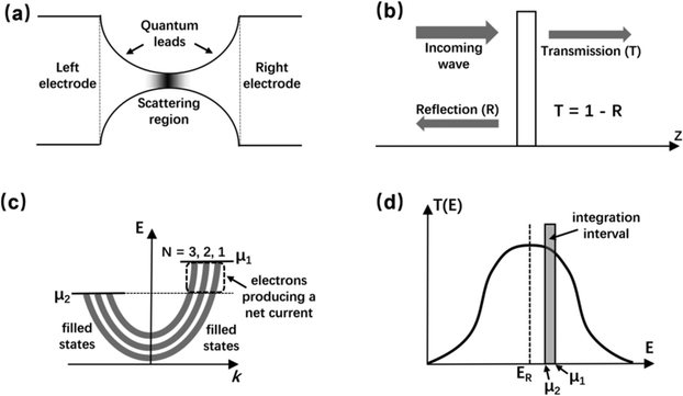 | ||
| Fig. 4 Model of the quantum transport in a nanodevice.54,55 (a) Schematic picture of an APC. The scattering region is connected to the electrodes through the quantum leads; (b) reflection and transmission amplitudes; (c) energy band diagram of a ballistic device with a finite number of populated 1D sub-bands; (d) energy interval over which the transmission must be integrated to obtain the overall current. | ||
The one-dimensional sub-band between μ1 and μ2 can be used as a channel for propagating electrons (Fig. 4c),55 in which case the intermediate scatterer can be seen as a potential barrier. If the two lowest discrete energy levels are spaced E2–E1 sufficiently large such that all electrons fall within the one-dimensional sub-band of E1, this is an example of one conducting channel (Fig. 4d). The net current can be expressed as
when T(E) = 1 and N is the number of conductive channels. The conductance is
Usually, the conductance of a single-channel perfect wire with spin is called the quantum conductance54
3. Nanoionics-enabled construction of the APC structures
Nanoionics is an emerging research field focused on the study of ion transport in solid-state nanosystems. It plays a pivotal role in facilitating technological progress, particularly in information technology and energy sectors, where the use of ions as charge carriers has garnered significant attention. In recent years, researchers have successfully demonstrated the construction of APC structures within solid-state nanosystems, which has attracted considerable interest due to its advantages such as high efficiency, reconfigurability, and excellent compatibility with CMOS technology.25 In nanoionics-constructed APC structures, the electric field is used to control the distribution of ions at the atomic scale, allowing the APC structure to be reconfigured. Specifically, the electric field induces redox reactions and ion migration within the heterojunction, composed of electrode/solid electrolyte/electrode multilayers, thereby forming a nano-conductive channel connecting the top and bottom electrodes. By precisely controlling the dimensions of this nano-conductive channel, APC structures can be constructed, enabling the observation of the quantum conductance effect at room temperature.56,57APC structures can be classified into two principal categories according to the types of migrating ions involved: metallic type and vacancy type. Metallic-type APC structures are typically formed by the migration and redox reactions of active metal cations injected from the electrode. During operation, the electric field induces the migration of metal cations in the solid electrolyte, where they undergo electrochemical reactions to deposit as metallic atoms or clusters, thereby forming conductive channels between electrodes. In contrast, vacancy-type APC structures are constructed by the formation of vacancies induced by the migration of anions within the solid electrolyte. When anions migrate under an electric field, vacancies are created in the lattice structure. These vacancies can act as effective atomic-scale constrictions, exhibiting quantum conductance effects when they are appropriately controlled. The formation and annihilation processes of both types of APC structures involve complex electrochemical interactions and ion movements within the solid electrolyte. These processes are crucial for developing advanced nanoelectronic devices and exploring quantum phenomena at the atomic level.
3.1. Evolution dynamics of the APC construction
As shown in Fig. 5a, the schematic diagrams illustrate the redox reaction of Ag+ and the formation of Ag APC structure within the Ag/polymer/Au heterojunction.60 Subsequently, a negative bias was applied to the active metal electrode following the establishment of nano-conductive channels. A similar redox process occurs within the metal nano-conductive channel. Metal atoms progressively detach from the nano-conductive channel, leading to a reduction in its lateral dimension. The APC structure gradually thins and completely disintegrates. By alternately applying positive and negative voltages, the metallic APC structure undergoes repeated formation and dissolution, facilitating the reconfiguration of atomic structures. Aono et al. fabricated a Pt/nanogap (1 nm)/Ag2S/Ag heterostructure following this principle, as shown in Fig. 5b. They applied a positive voltage to the Ag electrode, enabling Ag+ to be reduced to Ag atoms at the nanogap between Ag2S and Pt. By managing the growth of Ag atom clusters on the surface of Ag2S under the electric field, the size of the contact could be controlled between Ag atom clusters and the Pt electrode. This controlled process ultimately allowed for the construction of an APC structure.15 Furthermore, Nandakumar et al. designed a SiO2-based device with a Cu top electrode for the low-temperature back-end-of-line (BEOL) process integration as displayed in Fig. 5c.61 The device demonstrated a quantized conductance effect, where the lateral dimension of the nanofilament was estimated by modelling a single filament and measuring the voltage drop across the device during conductance transitions. Experimental results revealed that the device displayed quantization conductance at half-integer multiples of G0 due to the presence of energy sub-bands in the Fermi level split between contact reservoirs. In addition, Yang et al. proposed a technique called electrochemically assisted mechanically controllable break junction (EC-MCBJ) to construct APC structures (Fig. 5d).62 The suspended electrode pairs were first patterned and fabricated on the Si microchips by employing traditional photolithography and wet-etching processes.62 Subsequently, a new alkaline electroplating solution was employed to create Cu nanocontacts between these electrode pairs. By a continuous electrochemical deposition process, the width of the fabricated Cu nanocontacts was reduced to less than 18 nm, leading to the production of numerous Cu quantum point contacts. Overall, this EC-MCBJ method shows many advantages as a novel approach for constructing atomic-scale devices.
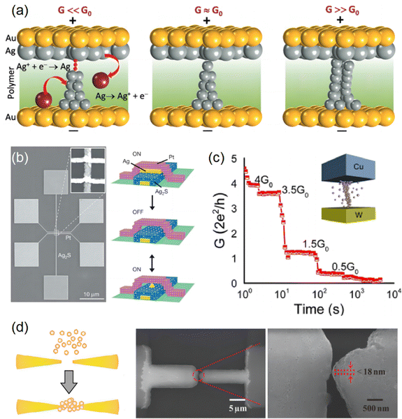 | ||
| Fig. 5 Metallic-type APC structures. (a) APC structures were constructed through Ag ion migration and electrochemical processes.60 (b) SEM image and Ag ion migration process of the Pt/nanogap (1 nm)/Ag2S/Ag heterostructure.15 (c) APC structures and quantum conductance effects in the Cu/SiO2/W device based on Cu ion migration.61 (d) The fabrication of the APC structures through an electrochemically assisted mechanically controllable break junction (EC-MCBJ) method.62 | ||
Here, the detailed formation and dissolution processes of vacancy-type APC structures were illustrated, as shown in Fig. 6a.64 In this process, inert materials are used as the top and bottom electrodes. When a positive bias is applied to the top electrode (anode), the O2− ions from the solid electrolyte migrate towards the top electrode, resulting in the formation of oxygen vacancies within the solid electrolyte. As these vacancies rearrange, a nano-conductive channel is formed from these vacancies, significantly increasing the heterojunction conductance (G ≫ G0). Subsequently, the O2− ions near the nano-conductive channel undergo electrochemical reactions when applying a negative bias to the top electrode, leading to the dissolution of the nanostructure. As the negative bias increases, the lateral dimensions of the nano-conductive channel decrease to form an APC structure. At this stage, the heterojunction conductance stabilizes around G ≈ G0. The APC structure is completely broken after further increasing the negative bias, resulting in a small heterojunction conductance (G ≪ G0). Similarly, the reconfiguration of the vacancy-type APC structure can be realized under the alternating action of positive and negative voltages.
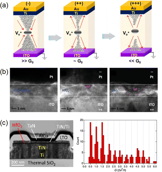 | ||
| Fig. 6 Vacancy-type APC structures. (a) APC structures were constructed through oxygen ion migration and electrochemical processes.64 (b) HRTEM images of the partially and fully developed oxygen vacancy conductive filaments.65 (c) TEM image of the cross-sectional view of the TiN/Ti/HfOx/TiN device. Histogram of conductance plateau values retraced from 330 reset operations.66 | ||
To gain a deeper understanding of the formation of the structure, the composition and nanostructure of nano-conductive channels are usually verified using transmission electron microscopy (TEM), energy dispersive spectroscopy (EDS), and other analysis methods. For example, Xue et al. employed high-resolution TEM (HRTEM) to analyze partially and fully formed oxygen vacancy conductive filaments.65 Their study demonstrated that 32 discrete quantum conductance states could be repeatedly tuned by controlling the O2− ion migration. The dissolution process of atom-sized oxygen vacancy filaments within the Pt/HfOx/ITO structure was also observed using voltage pulses (Fig. 6b). Furthermore, Peng et al. selected HfOx as the solid electrolyte and constructed a TiN/Ti/HfOx/TiN valence-change device,66 which was analyzed under a HRTEM, as shown in Fig. 6c. The appearance of half-integer multiples of G0 instead of only integer multiples could be attributed to several factors, including differences in chemical potentials between the two carrier reservoirs along the filament, reconfiguration of atomic contacts, and the potential impact of weak magnetism due to oxygen vacancies. With carefully controlled conditions, a stepwise decrease in conductance from 9 to 0.5 G0 in steps of 0.5 G0 could be successfully achieved using pulse-mode reset procedures. These experimental results underscore the importance of monitoring the measured bias voltage to evaluate the quality of the device preparation and measurements employed in the study of conductance quantization, which will facilitate future advancements in device design and fabrication.
Both metallic and vacancy-type APC structures have been successfully constructed in various solid electrolytes, including polymeric materials, metal oxides, metal sulfides, two-dimensional (2D) graphene, and silicon dioxide materials. A comparative analysis of these two types of APC structures shows that their stability is significantly influenced by the ion migration activation energy. Higher migration activation energy reduces spontaneous ion diffusion, thereby enhancing the stability of the APC structures. Typically, the O2− ions in the oxide medium exhibit higher migration activation energy compared to Ag+, Cu2+, and other active metal ions. For example, the migration activation energy of O2− ions in ZnO is approximately 2.4 eV, while for Ag+ and Cu2+ ions, it is only 0.9 eV and 1.4 eV, respectively. Thus, vacancy-type APC structures offer better control and stability of quantum conductance states than metallic-type APC structures. Moreover, statistical analyses show that vacancy-type APC structures tend to exhibit quantum conductance with both integer and half-integer multiples of G0, whereas metallic-type structures are more likely to display conductance in integer multiples of G0.56 This difference may be attributed to the inherent conductance properties of the two types of structures. As a result, vacancy-type APC structures are more suitable for achieving higher-density storage. Furthermore, due to the higher migration and activation energies of vacancies, vacancy-type APC structures typically require a higher driving voltage to maintain better stability.
Recently, Emboras et al. engineered 1D Ag atomic chains within heterojunctions that exhibited memristive characteristics, effectively integrating electrons and photons.71 By utilizing the interplay between electrons and photons to manipulate the APC structure, they realized ultra-sensitive photodetection at the atomic scale, as depicted in Fig. 7a. Under the electric field, Ag atoms undergo migration and redox reactions, leading to the lateral diffusion of Ag ions and the formation of conductive filaments. The elevated optical signal power may locally heat the system, thereby amplifying the electrochemical processes and modifying the structure of the conductive filaments, generating the APC structure. Furthermore, a histogram covers conductance values ranging from a fraction of G0 up to multiples. Visible peaks appear around integer multiples of G0 (1, 2, 4, and 5 G0), indicating that the fabricated Ag-α-SiO2-Pt device operates at the atomic scale and involves the relocation of only a few atoms. The slight deviations observed in conductance from integer values of G0 are attributed to contact resistance effects, as well as defects and impurities at the Ag/Pt interface, which cause electron wave scattering and energy loss. Besides, Milano et al. investigated the morphological transformations of individual Ag nanowires with memristive properties during breakdown as shown in Fig. 7b.72In situ scanning transmission electron microscopy (STEM) measurements were conducted to observe the detailed process. Molecular dynamics simulations revealed four distinct stages in the dynamic evolution of conductive filaments: (I) the migration of Ag atoms along the edges of the nanowires under the influence of an electric field; (II) the nucleation and subsequent growth of Ag atoms; (III) the formation of Ag conductive filaments bridging the nanowire ends; and (IV) the lateral expansion of these Ag conductive filaments. This comprehensive analysis provided deeper insights into the mechanisms that govern and regulate ion transport in APC structures.
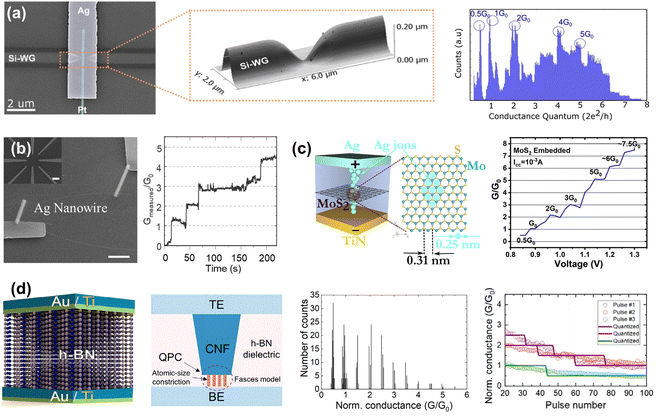 | ||
| Fig. 7 Quantum conductance of APC structures in (a) and (b) 1D and (c) and (d) 2D materials. (a) SEM picture of the atomic photodetector. The atomic force microscopy image of the device before the deposition of the metals and a vertically oriented 3D waveguide tip (left). Histogram of optically induced conductance quantization (right).71 (b) SEM image of a single nanowire device obtained by connecting an Ag nanowire to a pre-patterned electrode using IBID deposition of Pt contacts (scale bar, 10 mm). The inset shows a low-magnification SEM image of the pre-patterned sub-millimetric probe circuit (scale bar, 50 mm). Quantum conductance effect in the nanowire device.72 (c) Quantum conductance effect in the Ag/SiO2/MoS2/SiO2/TiN structure with 2D MoS2-embedded in the device and quantum conductance of the device after applying a DC bias of 1.3 V.73 (d) Schematic of the memristors fabricated using an h-BN dielectric and histogram of the normalized conductance.74 | ||
Quantum conductance is generated through the formation of atom-level conductive channels. The 1D materials provide significant dimensional advantages in constructing the APC structures through simple mechanical stretching. As bottom-up building blocks, 1D structures provide key benefits such as ultimate scalability, high spatial localization of switching events, and a large surface-to-volume ratio, which can be harnessed to modulate electronic and ionic transport properties. The varying Schottky barriers between nanowires and electrodes in these devices enable self-limited currents, reducing the risk of Joule heating.75 Furthermore, short-term plastic effects can be modeled using the enhancement–inhibition rate balance equation commonly seen in ion transport kinetics.76
Over the last few years, 2D nanomaterials have garnered significant attention due to their distinctive physical and electronic properties, holding great promise for advanced electronics. Many nanodevices now incorporate solid-state or 2D materials as dielectric layers in vertical structures, where the active layer is sandwiched between two electrodes.77 In such designs, the APC structures are typically formed by ion migration through the 2D material dielectric layer under the influence of an electric field. The wide variety of available 2D materials offer extensive options for constructing APC structures. By exploring the interaction mechanisms between ions and these materials, advanced nano-ionic devices have been designed and fabricated.78,79 Furthermore, the atomic-level thickness of 2D materials and the weak van der Waals forces between layers contribute to their exceptional potential in electronics, providing superior downscaling capabilities, easy stackability, and compatibility with traditional silicon-based devices.80
In previous works, memristors have usually been fabricated using bulk materials and constructed into a sandwich structure, where electric fields facilitate the transport of active ions and the formation of APC structures. The quantized conductance observed in these devices arises from the minimal size of the APC structures, leading to resistive switching phenomena. 2D materials have potential as alternative materials for sandwiched memristor devices because of their many merits. As illustrated in Fig. 7c, Kitsios et al. investigated the resistive switching behavior of a thin SiO2 layer embedded with 2D MoS2 in a conductive bridge random access memory (CBRAM) configuration.73 The device demonstrated enhanced conductance quantization, exhibiting eight distinct quantized conductance states during direct current (DC) operation, which increased to 10 states under pulse measurements. To further understand the mechanism, the kinetics of Ag in relation to the recorded variability was studied. It was observed that the presence of MoS2 thin films induces a sieving effect, confining Ag atoms as they traverse the films, thus limiting the conductive channel during its formation. Consequently, the diameter of the conductive channel approaches that of a quantum wire structure. As Ag atoms pass through multiple layers of MoS2 thin films, they exhibit a dendritic morphology, leading to the formation of multiple conductive channels and fluctuations in variability. This condition also affects quantum conductance, leading to the manifestation of non-integer values.
Quantum conductance can realize multifaceted operations, significantly enhancing both efficiency and precision. Besides regulating ion transport to establish APC structures within the 2D MoS2, the hexagonal boron nitride (h-BN) has an atomically smooth surface free of dangling bonds and remarkable tensile strength,81 showing great potential applications. These characteristics make h-BN highly compatible with CMOS circuits and flexible switching devices. Roldan et al.74 fabricated an Au/Ti/h-BN/Ti/Au device using h-BN as a dielectric layer. The vertical control of the APC structure was achieved through the regulation of ion transport and redox reactions under an electric field as presented in Fig. 7d. By employing the quantum point contact model to analyze obtained experimental data, it was found that the resistance of the device increased as the number of channels decreased during the reset process. Initially, a significant decrease in current was observed in the pulse train, but it eventually saturated, corresponding well with quantized conductance values. The normalized conductance (G/G0) tends to converge to half-integers or integers. This procedure was repeated for all pulse trains, and a resultant histogram was computed, revealing observable conductance quantization.
2D materials encompass a variety of semiconductors and insulators. Unlike traditional oxides with thicknesses of just a few nanometers, 2D materials have periodically arranged lattices, allowing them to function as atomic sieves that control ion diffusion barriers and lead to more stable APC structures. Additionally, 2D materials can form heterojunctions with other materials, where the interlayer coupling strength can be modulated by van der Waals forces. This modulation facilitates the construction of high-quality APC structures across different materials. Furthermore, the diverse band gap characteristics of 2D materials provide better control over quantum tunneling effects, offering a pathway to generate multiple quantum conductance states.
3.2. First-principles calculations of nanoionics enabled APC structures
Since DFT cannot be applied to open systems and is not a non-equilibrium theory, Taylor et al. established the first-principles calculations by DFT within the framework of nonequilibrium Green's function (NEGF) theory to address the above issues and produced the quantum transport package McDCal.82 Over the past few decades, the NEGF method has been developed to investigate and predict the transport properties of nanoscale materials, as well as the operation and performance of nanoscale devices.83 The implementation of transport theory has been combined with existing computing software for electronic structures, e.g. Nanodcal,82 TranSIESTA,84 SMEAGOL/Gollum,85 GPAW,86 Atomistic NanoTransport,87 ASE,88 ATK.89 The electric current can be evaluated using the Landauer–Buttiker formula:55Here, f1 and f2 denote the Fermi distributions in the left and right contacts, respectively
| T(E) = Tr[ΓL(E)Gr(E)ΓR(E)Ga(E)] |
At present, the calculated conductance and I–V curves of the APC structure can be obtained by examining the transport properties from the transmission spectra at the zero or continuous bias voltage based on the first-principles electron transport simulation, DFT+NEGF method.90 For example, the APC structure of metal ions in Ag/PEO/Pt devices exhibited reproducible quantized conductance ∼1 G0 in I–V measurements. A symmetric three-atom chain with different numbers of Ag atoms in the channel region was constructed to explain the experimental observations. The calculated conductance of single-atom (two-atom) point contact was ∼1 (2) G0 and dropped quickly to <1 G0 when extending the tunneling gap (Fig. 8a).91 Besides, ordered vacancy filaments of atomic thickness can form a transmissive channel between two metal contacts, which can also exhibit quantized conductance.92 By removing the adjacent oxygen atoms in HfO2, a metallic oxygen vacancy (Vo) filament penetrates the entire oxide film (Fig. 8b),93 and the calculated conductance values are 1.02 and 1.13 G0, consistent with the experimental distribution of the conductance of the intermediate states, which has a peak at 1 G0.94 When an oxygen atom moves into the filament, the conductance decreases exponentially. With the oxygen at the fourth oxide layer, the conductance becomes two orders of magnitude smaller than the open Vo filament. Along with one oxygen atom moving from position 5 to the center (position 8), two one-dimensional potential wells of Vo filament in 15 HfO2 layers become identical, and the conductance increases quickly from 10−3 to 0.31 G0 for the resonant transport. The resonant tunneling of the discontinuous vacancy filament could significantly alter the magnitude of quantum conductance, which provides an idea for the use of single atom control to realize resistance change based on the conductive mechanism of oxygen vacancies.
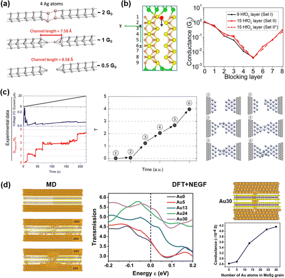 | ||
| Fig. 8 First-principles simulation of quantum conductance. (a) Atomic configuration of a three-atom chain with single-atom (two-atom) point contact and tunneling gap.91 (b) Optimized atomic structure of a Pt/9-layer HfO2/Pt device and evolution of the device conductance as an oxygen atom blocks the Vo filament at different atomic layers.93 (c) Quantum conductance effects in a current sweep-induced nanowire rewiring, and evolution of the transmission coefficients and atomic structures during the rewiring process computed by DFT simulations.72 (d) MD simulation of Ag migrating in multilayer MoS2, plot of zero-bias transmission spectra calculated for device configurations, the structure of 30 Au (Au30) atoms placed randomly inside the grain boundary regions of MoS2, and the change in electrical conductance with the number of Au atoms in MoS2 grains.95 | ||
Beyond the APC structures derived from manual construction or experiments, molecular dynamics (MD), based on Newton's laws of motion, can provide complex structures that change continuously over time. Subsequently, the quantum transport simulations can investigate the correlation between observed integer multiples of the fundamental quantum conductance and distinctive dynamic trajectories of filament atomic reconfiguration. By EchemDID MD,96 the external voltage effect is considered by changing the electronegativities of the atoms in the bottom and top electrodes. To simulate the rewriting process of Ag nanowires (Fig. 8c), typical atomic configurations extracted during filament evolution obtained from MD results are used to calculate the transmission coefficient T, where T = G/G0.72 The calculated conductance is close to 0 G0 before the conductive filaments are connected (structures 1 and 2). As the conductive filament thickens, the conductance gradually increases from 1 to 4 G0 (structures 3–6). The quantized conductance, referring to electrochemical processes and ionic dynamics, has been reproduced by quantum transport simulation, which would deepen the understanding of the relationships between the geometric shapes of nanofilaments and quantum conductance in APC structures.
The changes in quantum conductance in the filament formed by the injection of active metals into the dielectric material can also be modelled by first-principles methods. In the monolayer MoS2, the adsorption of metal ions in the point defects of the 2D layer can explain the resistance switching mechanism from the HRS to the LRS.97 As shown in Fig. 8d, a MoS2-based bilayer metal–insulator–metal (MIM) device was built, where grain boundaries existed in the middle of the MoS2 layers.95 At 0 V, the device remained in the HRS with slight changes. As the voltage increases, the surface Au atoms dissolve due to the difference in charge. At a certain voltage, the atoms in the electrodes start to move through the grain boundary. As the voltage increases, more Au ions move into the grain boundary, forming a conductive filament. The device switches to the LRS when the Au ions connect the two electrodes. Furthermore, a model of two layers of MoS2 and four Au layers on both sides was also built for electron transport calculations, which showed that the conductivity increases with the number of Au atoms, from ∼2.8 to ∼4.1 × 10⁻⁴ S (about 4–5 G0). Adding less than 5 Au atoms to the grain increases the conductance slightly because the Au atoms have not created a conductive path. As the number of Au atoms increases from 5 to 24, the conductive filaments form and thicken, causing the conductance to change. When the number is increased to 30, the conductance saturates as the filaments become sufficiently thick. The calculation demonstrates how the conductance evolves during the formation of conductive filaments.
4. Modulation of the quantum conductance in APC structures
The intricate atomic-level structure of atomic point contact (APC) structures, composed of a minimal number of atoms, makes them highly sensitive to applied physical fields that influence their quantum conductance states. Previous studies have shown that electric and magnetic fields can alter electron energy levels and tunneling probabilities.98 In addition, the stress field can modulate the atomic spacing and lattice structures, thereby optimizing the electron transport pathways.99 Temperature gradients can induce thermoelectric effects and thermoelectric conversion, further influencing conductance behavior.100 Therefore, the dynamic regulation of quantum conductance through these multi-physical field approaches will enhance the functionality and flexibility of devices, paving the way for the development of high-performance, low-power quantum information devices.4.1. Quantum conductance modulation under non-electric fields
Multiple external physical fields have been used to modulate the quantum conductance effects. Recently, Zhang et al.13 reported an atomic-scale metallic contact structure by precisely stretching an Au wire. They employed a commercial light-emitting diode (LED) lamp as the light source to adjust the quantum conductance of the constructed APC structure (Fig. 9a). The conductance increased from 10−5 to 80 G0 with a delay of 1–2 s upon light stimulation. Conversely, the conductance decreased to below 1 G0 after the light was turned off. As depicted in Fig. 9a, the localized plasmon resonances of the nanogaps resulted in significant light absorption in the visible and near-infrared region, involving quantum tunneling effects.101,102 The absorbed light was converted into thermal energy, causing the nanoelectrodes to expand and reconnect. When the system achieved thermal equilibrium, the conductance reached its maximum value. As the light intensity diminished, the metal wire stretched due to electrode shrinkage, resulting in the separation of the electrodes once more after the light was fully extinguished.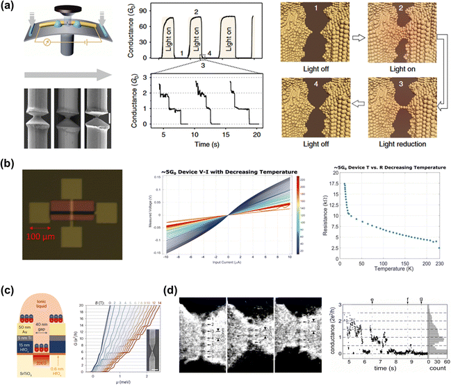 | ||
| Fig. 9 Impact of various physical fields on quantum conductance. (a) A schematic representation of the atomic-scale metallic contact using the MCBJ technique, and SEM patterns of the notched microwire during the stretching process (left). Real-time measurement of the current with the light switched on/off and the corresponding conductance values as the light intensity changes (middle). Schematic of the atomic arrangement, which corresponds to four conductance states upon light illumination (right).13 (b) Microscopic image of the Cr/Au/TiO2/TiOx/Cr/Au device (left). The V–I plot and variation of resistance with current input and decreasing temperature when the device is set to 5 G0.103 (c) Schematic cross-section of the constriction region. The red and blue dipoles represent the polarized layer of ionic liquid molecules (left). Zero-bias conductance G as a function of gate voltage (converted to chemical potential μ), with magnetic field B tuned between 0 and 14 T (right).104 (d) HRTEM images of Au ASWs showing the average interatomic distance (0.30 nm), minimum interatomic distance (0.25 nm), and maximum interatomic distance (0.40 nm). Contact conductance during the tensile deformation as a function of time and the corresponding histogram.99 | ||
The thermal expansion effect induced by light fields in metal nanowires allows for the reconstruction of the APC structures, enabling precise control over changes in conductance states. Since electrons act as carriers for both heat and electric current, electrical and thermal conductance in metals are interconnected at the macroscopic scale.105 Exploring thermal transport in atomic-dimensional junctions is essential for grasping the quantum phenomena of energy transmission.106,107 Köymen et al.103 explored the relationship between quantum conductance properties and temperature for Cr/Au/TiO2/TiOx/Cr/Au memristive devices as presented in Fig. 9b. Nonlinear behavior in the current–voltage (I–V) characteristics could be observed due to the insulating nature of TiO2 and the presence of inversely polarized Schottky barriers at the metal–insulator interfaces as the ambient temperature decreases from 290 to 18 K in the pristine device. Their analysis confirmed that resistance increases with decreasing temperature, both in the pristine state and in resistance states approaching the quantum conduction regime. In addition to temperature, external magnetic fields also affect the quantized conductance values in the APC structures. Strontium titanate (SrTiO3), a perovskite oxide known for its electrostatic tunability, superconductivity, and spin–orbit coupling, shows promise for the development of quantum device. However, exploring quantum effects in SrTiO3 nanostructures is challenging because of inherent disorder. Mikheev et al. reported high-mobility, gate-tunable devices based on SrTiO3 with a thin hafnium oxide (HfOx) barrier layer, as shown in Fig. 9c. These devices demonstrated ballistic constrictions and precise quantization of conductance in the normal state.104 The presence of a magnetic field caused a sequence of sub-band degeneracies due to electron mass anisotropy. The analysis of the first conductance step in line traces of G revealed that the twofold degeneracy of this step persisted up to a magnetic field of approximately 7 T. Beyond this, the twofold degeneracy was broken, and the magnitude of the first few conductance steps became half of G0 at higher magnetic fields.
Understanding the role of strain in modulating conductance is crucial for analyzing the effects of various mechanisms on conductance. Previous studies have demonstrated that strain can significantly impact ballistic conductance. For example, Hossain et al.108 revealed that in a graphene-based device, applying uniaxial compression to the graphene sheet within a lead–graphene-lead configuration maintains its unstrained ballistic conductance properties for electrons with energies exceeding the system's Fermi energy threshold. In contrast, for all other strain conditions, regardless of the electron energy, graphene's ballistic conductance will either increase or decrease depending on the specific type of strain.
For Au nanometer-sized contacts, the conductance decreases in a stepwise manner during the thinning process, with each conductance level corresponding to approximately integer multiples of G0.109 Kizuka explored the fluctuation in atomic configuration during the formation of Au APC structure through the integration of in situ HRTEM with conductance and force measurements (Fig. 9d).99 Notably, the APC structure comprising five atoms exhibited a stable conductance state of 1 G0, despite fluctuations ranging between 0.1 and 1.5 G0. However, a reduction in conductance below 0.1 G0 was observed as the number of atoms exceeded five. These findings provide compelling experimental evidence for the atomically localized structures in APC systems and reveal a direct correlation between these structures and their mechanical and electrical properties.
4.2. Quantum conductance modulation under the electric field
The electric field plays a pivotal role in the modulation of the APC structures. Particularly, the quantum conductance effects induced by nanoionics are strongly influenced by the underlying ionic electrochemical and dynamic processes under the electric field. It has been shown that the shape of the atomic-sized contact and the growth direction are determined by the interplay between the electrochemical reaction rate and ion mobility within the solid electrolyte.110 These factors can be effectively controlled through various parameters such as driving forces (e.g., current or voltage sweeps), compliance current (Icc), stop voltage, and sweep ramp rates. Consequently, these controls allow for precise modulation of the corresponding quantum conductance levels.The influence of driving forces on quantum conductance effects, such as current and voltage sweep stimulation, has been widely explored. Köymen et al. applied slow current and voltage inputs in the Cr/Au/TiO2/TiOx/Cr/Au devices during the formation and annihilation processes of the APC structure, respectively.103 They applied slow current and voltage inputs and simultaneously monitored the current–voltage trends, observing quantum conductance steps induced by these electrical inputs. Additionally, a detailed statistical analysis of the quantum conductance effects was conducted for both methods. Current sweep stimulation caused step-like changes in the measured voltage, corresponding to the formation of APC structures and resulting in discrete steps in device conductance. More readily and frequently distinct integer conductance levels could be achieved, which is mainly related to the current-enhanced stability effects involving the interplay between surface tension and quantum pressure forces on the APC structure. This phenomenon has also been reported in other traditional MIM heterojunctions based on thin films with Ag electrodes and in single metallic nanowires such as Ag.111 During voltage sweep stimulation, both distinct integer and half-integer conductance levels were detected, achieving a wider range of quantized conductance states.
Experimental results indicate that quantum conductance levels can be accurately modulated by appropriately tuning the programming parameters. For example, a higher Icc of 400 μA was used to obtain 2.5 G0, while lower conductance levels of 1 G0 can be achieved by reducing the Icc to 100 μA.72 Zhu et al. reported a similar approach for quantum conductance regulation, achieving a monotonic increase in conductance states.112 They first achieved a quantum conductance state of 2.5 G0 with an Icc of 100 μA, which then increased to 4.0 G0 with an Icc of 250 μA, followed by 4.5, 6.5, and 8.5 G0 with further enhanced Icc values. This is because the higher Icc tends to generate a strong and thick APC structure, which allows more sub-bands for electron ballistic transport. Notably, similar quantum conductance levels can be realized with different Icc values across various devices or even with the same structure. Besides, a similar behavior was also observed in the annihilation process of the APC structure by controlling the stop voltages. For instance, the initial conductance of the device was first switched to 20 G0 and then several distinct quantum conductance levels of 2, 1.5, 1, and 0.5 G0 can be obtained as the stop voltage increases.26
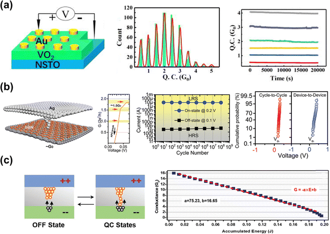 | ||
| Fig. 10 Performance optimization of quantum conductance in APC structures. (a) Schematic of the Au/VO2/NSTO device structure with Nb-doped SrTiO3 (NSTO) as the substrate and the bottom electrode (left). Histogram of quantum conductance at 50 reset point cycles (middle). Polymorphic holding properties of quantum conductive states (right).113 (b) Schematic of a single-atom point-of-contact switch device and quantized conductance states (left). Endurance test using a voltage pulse with an amplitude of 1 V and a width of 1 μs (middle). Cumulative probability of threshold voltage in cycle-to-cycle (red) and device-to-device (blue) measurements (right).114 (c) Schematic of controlled APC structure evolution via oxygen ion migration in an asymmetric Pt/HfOx/ITO device (left). Conductance versus cumulative device energy (right).65 | ||
5. Applications
To date, the APC structures have been constructed using a variety of materials and configurations, showing significant potential for the design and manufacture of information devices. These unique structures enable controllable electron transport at the nanometer scale and facilitate the creation of highly integrated and miniaturized electronic devices. Moreover, the APC structures allow for the control of single electrons and precise quantum states, enhancing the operating accuracy and stability of devices. By reducing resistance and energy loss through quantum tunneling, APC structures improve energy efficiency and reduce power consumption. The quantum conductance generated by electrons passing through the APC structures also offers numerous advantages in the information field. It enables charge transport at discrete energy levels, reducing scattering effects and increasing conductivity efficiency. The discrete energy level characteristics of quantum conductance minimize energy loss. Related devices based on quantum conductance also exhibit fast response, which boosts the speed of information processing. Quantum conductance transmission accommodates thermal noise and other forms of electronic noise, improving signal clarity and reliability. These properties enable efficient information processing that surpasses the capabilities of classical computing. These advantages suggest that quantum conductance provides broad application prospects for future high-performance, low-power information devices. The applications of quantum conductance in the APC structures in different fields are described in detail below.5.1. Memory
The multilevel quantum conductance generated in APC structures can be utilized for multilevel data storage and the construction of logic circuit elements, offering advantages such as high density, low power consumption, and fast response speed. This is significant for achieving high-density information storage and logic operations. Leveraging quantum conductance enables the design of novel storage devices and computing modes, which creates great development space for information technology. Krishnan et al.116 incorporated the Ag salt into a polyethylene oxide (PEO) film to create a solid polymer electrolyte (SPE). This SPE was then placed between electroactive Ag and Pt electrodes to form a MIM structure, as depicted in Fig. 11a. The resulting device exhibited favorable resistance transition characteristics, earning the moniker ‘gapless-type atomic switch’. The resistance of the nanogap between the two electrodes fluctuates as wires are formed and broken. When subjected to an electric field, Ag atoms within the Ag/PEO/Pt devices undergo redox reactions and migrate within the polymer. This migration exhibits a highly controllable and reproducible quantized conductance behavior, confirming the well-controlled formation of the internal APC structure. The statistical histogram of conductance states reveals a distribution ranging from 1 to 10 G0 under voltage scanning, with prominent peaks observed at both integer and half-integer multiples. Specifically, the conductance states of ≥2 G0 exhibited a certain retention time; the retention time became longer for higher conductance values and is likely to increase exponentially with increasing conductance values. The maximum retention time of ∼1.9 × 10³ s was achieved for ∼9 G0. These numerous conductance states indicate promising prospects for the application of quantum conductance in polymer-based atomic switches for multilevel data storage.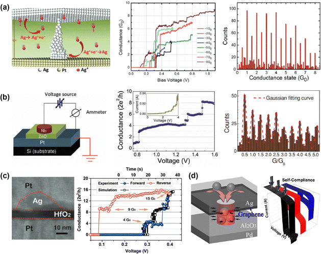 | ||
| Fig. 11 Quantum conductance for memory applications. (a) Schematic of the APC structures in the Ag/PEO/Pt device under forward bias (left). Multilevel quantum conductance states in the Ag/PEO/Pt device (middle). Conductance state histograms in G0 evaluated from 360 sweep cycles (right).116 (b) Schematic of a sandwiched Nb/ZnO/Pt structure (left). The quantum conductance step occurs during the set process in the Nb/ZnO/Pt device (middle). Histogram of conductance values of ITO/ZnO/ITO devices (right).112 (c) HAADF-STEM cross-sectional image of AND-TS stack layers and conductance quantization characteristics of the AND-TS device.117 (d) Schematic of the Ag/graphene/Al2O3-based TS device with self-compliance.118 | ||
In addition, Zhu et al.112 documented the conductance quantization observed in various oxide-based devices, including Nb/ZnO/Pt and ITO/ZnO/ITO systems. They demonstrated the ability to effectively modulate conductance quantization behaviors in these systems. The current jumps were initially observed during the set process of Nb/ZnO/Pt sandwich structures, corresponding to abrupt changes in conductance. Following each change, a stable platform was detected as shown in Fig. 11b. They suggested that this distinctive quantized conductance behavior is a common characteristic of RRAM devices founded on conductive filaments. Consequently, the study of quantized conductance behavior was extended to the ITO/ZnO/ITO device, which exhibited unipolar RS behaviors instead of bipolar switching observed in the Nb/ZnO/Pt device. The statistical histogram of conductance revealed that the values were concentrated near half-integer multiples of G0, similar to the bipolar resistance switching characteristics seen in the Nb/ZnO/Pt devices. These findings demonstrate that controllable atomic-scale conduction channels can be constructed in simple two-terminal devices in air and at room temperature, providing a platform for the development of new nano-devices based on quantum effects.
Selectors play a crucial role in mitigating leakage interference among storage cells within cross-point arrays, requiring high selectivity and minimal leakage currents to reduce sneak currents and power consumption. However, conventional selectors typically exhibit limited on-state currents (≤10 μA), which are inadequate for memory reset operations. Selector configurations like one-transistor-one-resistor (1T1R) compromise the scaling advantages of crosspoint architectures due to the large feature size of the transistor. In contrast, the one-selector-one-resistor (1S1R) configuration is better suited for x-point integration but suffers from high leakage current issues. Hua et al.117 addressed these challenges by developing Ag nanodots/HfO2-based selectors, where they directly observed significant jumps in quantized conductance at 4, 9, and 15 G0 by employing rapidly heat-treated Ag nanodots (Fig. 11c). Through exploiting the spontaneous rupture of delicate Ag filaments at the APC level with decreasing applied voltage, a selector could be achieved with a RESET current of approximately 2.3 mA, bi-directional threshold switching, no need for electrostatic formation, and exceptional selectivity exceeding 109. It also displayed ultra-low leakage current below 1 pA, a remarkably steep slope of 0.65 mV dec−1, and robust thermal stability up to 200 °C. Furthermore, this selector demonstrated notable rejection of leakage current and exceptional SET/RESET operation performance within a 1S1R configuration.
In another study, Song et al.118 introduced a technique involving the insertion of an engineered defective graphene monolayer between the Ag electrode and the Al2O3 electrolyte (Fig. 11d). This method effectively restricted Ag ion migration and controlled the size and density of Ag filaments, facilitating contact with Ag ions solely for the formation of an APC structure. Experimentally, they observed significant quantized conductance jumps from 11 to 21 G0. Capitalizing on these merits, they fabricated Ag/graphene/Al-based selectors with exceptional selectivity and adaptability, reaching levels on the order of 1010. These selectors exhibited an extremely low turn-off current of 0.1 pA and demonstrated switching slopes of 1.13 mV dec−1 and 1.11 mV dec−1 for on and off states, respectively. This work proved the significance of constructing an APC structure in the preparation of selectors with outstanding performance and minimal leakage current.
5.2. Computing
Except for multilevel data storage, quantum conductance within APC structures also holds promise for logic circuits. As leading candidates for advanced computing applications, memristors are being developed as key components in transient electronics. To date, the modulation of quantum conductance has been observed in memristors incorporating various metal oxides.119 Moreover, similar controllability has been demonstrated in transient materials. Zhao et al.120 presented a self-supporting lightweight memristor constructed from acidic polysaccharides as displayed in Fig. 12a. Due to the ability of Mg cations to interact with ionized acid groups, acidic polysaccharides can effectively confine ions. By utilizing these polysaccharides as the resistance-switching layer, enhanced precision in controlling conductive pathways can be achieved. In the Mg/pectin/Mg sandwich structure, 16 continuous quantum conductance states were achieved, measured in units of G0 (Fig. 12b). Remarkably, this quantum conductance switch presented an ultra-fast operational speed (2–5 ns) and low energy consumption (0.6–16 pJ). These properties positioned it as a promising candidate for incorporation into fast, low-power, high-density memory designs. Furthermore, the effective control of multiple quantum conductance states within a single device represented a significant advancement toward achieving quantized multi-bit storage and computing functionalities. Encoding stands as the primary mechanism of storage, facilitating the conversion of diverse forms of information such as words, images, and sounds into a storable format. This enables their recording, subsequent extraction, and utilization in subsequent storage stages. Zhao et al. further labeled the 16 quantum conductance states within a single Mg/pectin/Mg memristor as 16 distinct codes, with each code corresponding to a four-bit binary number. By employing two memristor units, they successfully encoded the sequence “NENU”, thereby conserving storage space (Fig. 12c).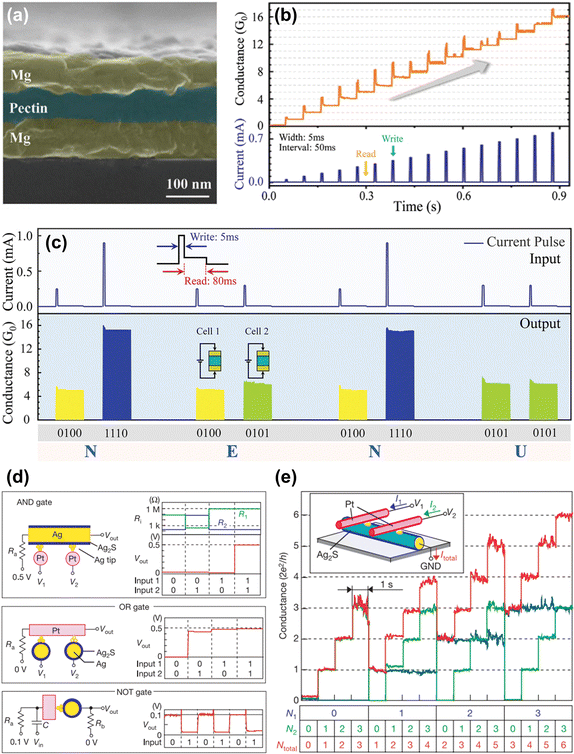 | ||
| Fig. 12 Quantum conductance for computing applications. (a) Cross-sectional SEM image of the Mg/pectin/Mg device. (b) 16 quantum conductance states were obtained by applying current pulses of different amplitudes. (c) Logic encoding of the word “NENU” according to ASCII.120 (d) Logic gates configured with the quantum conductance atomic switch (QCAS) made using Ag2S and Pt electrodes. (e) The conductance of each channel in a 1 × 2 array of QCASs was changed independently from 0 to 3 G0.15 | ||
Terabe et al.15 demonstrated that all requirements for a logic circuit, switching speeds exceeding gigahertz and operational voltages below 1 V, can be met through the utilization of the APC devices. They engineered a vacuum atomic switch using an Ag2S electrode and a Pt electrode, with an electrode spacing of 1 nm. Upon applying a forward bias to the Ag2S electrode, an Ag atomic bridge was formed between the two electrodes, inducing the device into a high-conductive state. Conversely, when a negative bias was applied to the Ag2S electrode, the Ag bridge disintegrated, resetting the device to a low conductive state. This atomic switch was then used to transition between two conductance states, enabling the realization of AND, OR, and NOT gates and facilitating the implementation of all fundamental logic operations as depicted in Fig. 12d. Moreover, the quantum conductance of the 1 × 2 atomic switching array was manipulated through the pulsed bias voltages, allowing for transitions between quantum conductance states. Each channel's conductance could be independently adjusted from 0 to 3 G0, enabling the system to function as an adder circuit and serve as a multilevel data memory capable of storing 16 states using only two switches (Fig. 12e).
The synapse serves as the functional connection point between neurons, playing a key role in information transmission. When a presynaptic action potential reaches the synaptic terminal, the voltage-gated calcium (Ca2+) channels are activated, promoting the influx of Ca2+ ions through the presynaptic membrane.121 This triggers changes in synaptic conductivity, resulting in the modulation of excitatory or inhibitory postsynaptic currents (EPSC/IPSC), a key mechanism in the propagation of information within the human neural network. Inspired by this biological process, developing synaptic devices that mimic these functions is essential for advancing artificial neural networks (ANNs), offering a promising alternative to conventional computing architectures.122 Ion-migration memristors, a common class of synaptic devices, predominantly rely on external electrical stimuli to induce the migration of metal ions or oxygen (or halogen) vacancies, leading to the formation of conductive filaments and atomic point contact (APC) structures.123 Reverse electrical pulses can drive the migration of these ions or vacancies in the opposite direction, disrupting the filament and modulating changes in electrical conductivity, closely mimicking the behavior of biological synapses. In their work, Ohno et al.124 proposed an Ag2S inorganic synapse device that exhibited a transient increase in conductance followed by a spontaneous decay to below 1 G0 when subjected to input stimuli at a lower repetition rate. Conversely, sustained conductance enhancement beyond 1 G0 is achieved with frequent input repetition. These findings suggest that individual inorganic synapse elements could serve as innovative functional components for neural systems that are capable of operating independently of software and pre-programming, unlike current artificial neural network systems. Meanwhile, they constructed a psychological model related to memory and forgetting processes, noting that the decay of conductance in the short-term memory (STM) mode mirrored the ‘forgetting curve’.
Compared to memristors based on metal oxides and chalcogenides, organic polymer-based electrochemical metallization (ECM) systems offer a promising avenue for precise control of conductive filaments at the atomic scale, enabling multilevel quantum conductance behavior under ambient conditions.125 Krishnan et al. reported an essential ion-conducting insulating layer using a polyvinyl imidazole (PVI) polymer for an Ag-PVI ECM-based memristor (Fig. 13a-c).60 The device exhibited stable resistive switching and highly controllable transitions from single to multi-level quantum conductance states with increasing stop voltage. The conductance stability exhibited an exponential increase, with a maximum retention time of approximately 50 minutes achieved for ∼10 G0 at room temperature. Moreover, the fabricated memristors successfully emulated diverse synaptic functions, including learning and forgetting behaviors. Simultaneous current–voltage and cyclic voltammetry studies revealed that the confined atomic redox process occurred within the narrowest region of the conducting channel in the Ag-PVI memristor. This study underscores the importance of quantum conductance in advancing the understanding and implementation of artificial synapses.
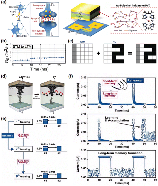 | ||
| Fig. 13 Quantum conductance for neuromorphic computing applications. (a) Schematic of the biological synapse illustrating the synaptic behavior between the pre-synaptic and post-synaptic neurons (left panel). Schematic of the Ag/Ag-PVI/Au device (right panel). (b) The transition from STM to LTM transition. (c) Schematic representation of memorizing the numerical letters “1” (STM) and “2” (LTM).60 (d) Schematic representation of the Ta2O5/HfO2 double-layer structure before and after Ag migration. The metal filament was formed by the 0.16 V/1 ms pulse but metal ions diffused after the pulse. (e) and (f) The transition from STM to LTM through the rehearsal with the repetitive training pulse of a pair 1.5 V/0.01 s. The right panel shows the initial state of the device and after the 7th and 8th training, respectively.126 | ||
A neuromorphic computing system emulates the neurons and synapses found in the human brain.127 It is adept at handling complex and unstructured information, enabling learning and memory processes through parallel chemical interactions. Recently, Lee et al.128 introduced a Pt/Al2O3/TaN device as a candidate for the neuromorphic device. During retention tests, the reset process consistently revealed a gradual decrease in current, supporting the existence of diverse multi-level states. The phenomenon of conductance quantization was further validated. The phenomenon of conductance quantization was confirmed, with the histogram plot showing a pronounced clustering around multiples or half-multiples of G0 across various conductance steps. Meanwhile, the values displayed discernible distinctions between 0.5 and 3 G0. To enhance the resolution and distinguishability of quantized values, it may be imperative to reduce the size of the conducting filament through techniques such as scaling down the device dimensions. The neuromorphic computing system was further developed using multi-level cells in Pt/Al2O3/TaN devices, where pulse measurements demonstrated continuous modulation of conductance through five cycles of potentiation and depression pulses. The I–V characteristic analysis during the set process showed an abrupt potentiation, while the depression phase followed a more gradual profile. By adjusting the pulse voltage amplitude, more gradual and symmetric conductance-change characteristics were achieved. Additionally, simulation results of MNIST pattern recognition utilizing this conductance data were presented, confirming that the conductance quantization phenomenon, observed during the reset process and pulse measurements, facilitated a more efficient learning process.
Jeon et al.126 proposed a unique Ta2O5/HfO2 double-layer structure, which effectively controls Ag ion diffusion due to the different oxidation ratios between the layers, as shown in Fig. 13d–f. The presence of distinct oxygen vacancy layers allowed precise control over the conductive filament, generating multi-level volatile switching and demonstrating the quantum conductance effect controlled by Ag atoms. During pulse measurements, the current levels decayed discretely, reflecting dynamics of the device's conductance over time. With repeated stimulation, the quantum conductance decreased from four to three steps , eventually transitioning to behavior consistent with classical physics. This shift highlights the device's ability to transition from short-term to long-term plasticity, a key feature of synaptic behavior. The double-layer device achieved an operating voltage of 0.2 V, an on/off ratio of 109, and a power consumption of 2 mW, outperforming previously reported devices that utilized metal-based oxides. These results highlight the significance of controlling Ag migration at the bilayer interface to enhance the synaptic properties and overall performance of neuromorphic devices.
5.3. Encryption
Nowadays, the advancement of the Internet of Things (IoT) necessitates the development of cost-effective, compact, lightweight, and dependable true random number generator (TRNG) circuits for encrypting data generated by objects or humans before transmission. State-of-the-art TRNG circuits typically utilize an entropy source to produce sequences of unpredictable binary numbers, exploiting phenomena such as the thermal noise of resistors, the jitter of ring oscillators, and the metastability of flip-flops (as shown in Fig. 14a).24 However, these circuits often suffer from high power consumption and limited scalability and are frequently confined to the simulation stage. Quantum conductance is driven by quantum mechanical effects, such as electron wave behavior and tunneling, which introduce uncertainty at the microscopic scale. This makes it possible to generate high-quality random number sequences by measuring conductance. Therefore, random number generators can harness the physical mechanisms of quantum conductance to provide a reliable source of randomness for information security and computing. Meanwhile, due to the polymorphic nature of the quantum conductance effect, it could be an efficient entropy source for TRNG circuits because they can produce random variations of different magnitudes during operation while consuming little energy.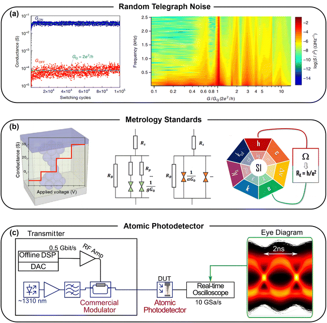 | ||
Fig. 14 Quantum conductance for random telegraph noise, metrology standards, and atomic photodetector applications. (a) Images showing “Random Telegraph Noise”: conductance switching data of a TaOx memristor for 100![[thin space (1/6-em)]](https://www.rsc.org/images/entities/char_2009.gif) 000 switching cycles showing larger variance in the regime close to a quantum of conductance, and a two-dimensional color plot showing S/I2 as a function of conductance G/GQ and frequency f at T = 295 K. The continuous scale on the color plot was obtained by linear interpolation between measured data points. This representation reveals the markedly increased noise near the first conductance quantum GQ and the tails of the noise distribution as a function of frequency.24 (b) Images showing “Metrology Standards”: the schematization of quantum steps in memristive devices,34 the equivalent electrical circuit of a memristive device,129 units and defining constants in the revised SI.130 (c) Images showing an “Atomic Photodetector”: a random bit-pattern at 0.5 Gbit s−1 was generated with an offline DSP and encoded by means of a commercial modulator onto a laser signal. The signal was then detected using the atomic scale photodetector.71 000 switching cycles showing larger variance in the regime close to a quantum of conductance, and a two-dimensional color plot showing S/I2 as a function of conductance G/GQ and frequency f at T = 295 K. The continuous scale on the color plot was obtained by linear interpolation between measured data points. This representation reveals the markedly increased noise near the first conductance quantum GQ and the tails of the noise distribution as a function of frequency.24 (b) Images showing “Metrology Standards”: the schematization of quantum steps in memristive devices,34 the equivalent electrical circuit of a memristive device,129 units and defining constants in the revised SI.130 (c) Images showing an “Atomic Photodetector”: a random bit-pattern at 0.5 Gbit s−1 was generated with an offline DSP and encoded by means of a commercial modulator onto a laser signal. The signal was then detected using the atomic scale photodetector.71 | ||
Nanoionic memristors with tunable conductance, capable of achieving multiple levels through the application of electrical stress sequences, represent a promising alternative.131,132 Song et al.133 developed a TiOx/Al2O3 memristor that utilizes random telegraph noise (RTN) as an entropy source. In this oxide-based memristor, charge transport is primarily controlled by trap-assisted tunneling at oxygen vacancies. The RTN signals are predominantly influenced by the current contribution of a single-dominant oxygen vacancy, resulting in two-level RTN signals. These RTN-induced current fluctuations are more observable at the low-conductance state (LCS), where device conduction is limited by the tunneling gap, corresponding to a quantized conductance value of about 2.5 G0. In contrast, at the high-conductance state (HCS), RTN signals are less pronounced due to the current flowing through a conductive filament in the switching layer, resulting in a lower conductance of 0.4 G0. Experimental results demonstrate that among the 60![[thin space (1/6-em)]](https://www.rsc.org/images/entities/char_2009.gif) 000 bits generated by the TRNG circuit, the percentages of 0 and 1 are 49.97% and 50.03%, respectively, indicating unbiased random bit generation. Furthermore, the TRNG remains functional in the digital mode even with multilevel RTN signals, as long as a dominant trap significantly influences device conduction compared to other traps. The generated random number dataset passed all 16 NIST tests, confirming its robustness and compliance with established randomness standards.
000 bits generated by the TRNG circuit, the percentages of 0 and 1 are 49.97% and 50.03%, respectively, indicating unbiased random bit generation. Furthermore, the TRNG remains functional in the digital mode even with multilevel RTN signals, as long as a dominant trap significantly influences device conduction compared to other traps. The generated random number dataset passed all 16 NIST tests, confirming its robustness and compliance with established randomness standards.
In addition, the 2D multi-layer h-BN was employed as an insulating layer to fabricate an Ag/h-BN/Ag memristor film by Pazos et al.,134 which exhibited exceptional RTN current signals. This h-BN-based memristor demonstrated low-power operation (approximately 650 nW) and retained highly stable RTN current signals for extended durations (exceeding 1 hour), marking one of the longest durations reported to date. Given their inherent time-domain randomness, the RTN signals generated by Ag/h-BN/Ag memristors hold promise for utilization in TRNG circuits, facilitating advanced data encryption and the generation of one-time authentication factors. Moreover, interfacing h-BN memristors with a commercial microcontroller led to the creation of a highly reliable and low-power standalone hardware solution for TRNG generation. This system exhibited robustness not only against temporary interruptions of the RTN signal but also against fluctuations in the characteristics of the entropy source.
5.4. Others
When the size of a conductor approaches the atomic scale, electrons undergo ballistic transport without scattering from each other, leading to the manifestation of quantum conductance effects. As the conductance quantum (G0 = 2e2/h) is determined solely by the fundamental constants of nature, it serves as a resistance standard, thus contributing to the revision of the International System of Units (SI) in 2019 (as shown in Fig. 14b).130 Unlike standard resistors, which are typically derived from the quantum Hall effect, those based on the quantum conductance effect can operate at room temperature, in ambient air, and without requiring a magnetic field, making them suitable for chip integration. Jordi Suñé et al.129 constructed a device consisting of Al2O3/HfO2/Al2O3/HfO2/Al2O3 nanolaminate insulators and Al as the top and bottom electrodes, respectively. This design uses the irreversibility of breakdown filaments, enhancing stability and facilitating statistical analysis of quantum conductance phenomena. The commercial resistors could achieve accuracies of up to 0.01%, while the uncertainty associated with the quantum Hall resistor standard was approximately 10−9. Despite these impressive standards, the sample-to-sample variation of around 15% when using quantum conductance was too large for this application. Although current results did not meet the required accuracy, optimizing insulator design and electrical stressing techniques could improve control over filament shape, potentially reducing sample-to-sample variations to levels suitable for resistive standard applications. These advancements are essential for integrating fundamental units on-chip and realizing self-calibrating systems with zero-chain traceability. Meanwhile, Delfanazari et al. achieved the first experimental observation of conductance quantization in a hybrid InGaAs–Nb APC structure.135 Repeatable quantized conductance was observed at zero magnetic fields across multiple quantum nanodevices fabricated on a single chip. These intrinsic properties make them invaluable for quantum metrology, particularly for establishing extremely precise and stable voltage standards.The inherent limitation of CMOS scaling can be addressed by using optical manipulation of atomic rearrangements within metal quantum dot contacts. This approach facilitates the development of optically controlled electronic switches by creating a platform that integrates electronics and photonics at the atomic scale (as shown in Fig. 14c). Recently, a pyramid-like 3D plasmonic tip composed of Ag-α-SiO2-Pt was fabricated by Emboras et al.71 By applying a bias voltage to the metal tip, they induced the formation of an atomic-scale filament that created a short circuit between the two metals. Subsequently, directing light onto a small area of the plasmonic tip caused reversible atomic movements between adjacent positions under illumination. These atomic rearrangements corresponded to transitions between different electronic quantum states. Despite its small size, the device exhibited impressive characteristics, including a notable resistive extinction ratio of 70 dB, a low shutdown current in the range of tens of picoamps, and reliable operation over weeks at room temperature. It delivered a characteristic hysteresis loop typical of a memristor driven by light rather than electricity, maintaining reliable performance over millions of operational cycles. Therefore, integrating the atomic point contact (APC) structure with electronics and photonics is promising for the development of innovative optoelectronic platforms, with potential applications such as digital photodetectors that bypass the need for decision-making circuits or analog-to-digital converters.
6. Summary and outlook
The development of reconfigurable atomic precision control (APC) structures through nanoionics technology offers a promising avenue for achieving atomic-level precision alongside quantum conductance effects. Several excellent review articles have thoroughly examined the advancements in these devices. Recent research underscores the growing interest in exploring one-dimensional (1D) and two-dimensional (2D) materials beyond the conventional oxide materials typically used for APC structure development. Additionally, studies on the influence of various external fields—including electric, optical, magnetic fields and mechanical stresses—on quantum effects within APC structures reveal their significant impact on quantum conductance. This review paper explores these aspects, aiming to deepen our understanding of the complex relationship between quantum conductance phenomena, materials' properties, and external fields, thereby contributing valuable insights into these rapidly evolving areas of research.So far, the resistance-switching devices (known as the memristors) have been considered promising for constructing APC structures and achieving quantum conductance. These devices generate conductive filament channels at the atomic level through ion migration within the dielectric layer, offering an efficient method for precise quantum conductance regulation. Over the past few decades, significant progress has been made in both the theoretical understanding and experimental observation of quantum conductance in APC structures within memristors. Memristors embedded with APC are valued for their ability to retain historical electrical signal information, ultra-low power consumption, ultra-fast response speeds, and precisely adjustable multi-level quantum conductance states. They are considered highly suitable for applications such as high-density storage, memory logic circuits, synaptic simulation, photon detection, and neuromorphic computing. They offer a promising strategy for managing the massive data growth of the information age.
However, the practical application of quantum conductance effects in APC structures still faces several challenges. The origin of stepwise variations in quantum conductance requires additional investigation to clarify the relationship between this phenomenon and discrete atomic structures. Moreover, improving the controllability and stability of quantum conductance states involves understanding the interaction between medium materials and migrating ions to achieve rational coupling of APC components and storage media. To precisely control and adjust quantum conductance levels, further exploration of the relationships between migrating ions, medium materials, operating parameters, and device functionalities is needed, which will guide future optimization of memristor performance. Additionally, it is crucial to pay close attention to other physical properties associated with quantum conductance states, including thermoelectricity, photovoltaics, superconductivity, and magnetoresistance effects. To enhance the reliability of device operation, it is imperative to develop advanced methods aimed at improving material quality and addressing defect characteristics in design. Besides, refining processing technology to achieve high crystallinity and uniform thickness of materials will help minimize sample variations. Future challenges include wafer-level device manufacturing, high-density integration, and multifunctional interconnection. Addressing these challenges will be crucial for the practical application of quantum conductance technology. Given its numerous characteristics and advantages, quantum conductance holds great promise for the information field, and ongoing exploration is expected to lead to rapid development and a wide range of applications in the near future.
Data availability
The data that support the findings of this study are available upon reasonable request.Conflicts of interest
There are no conflicts to declare.Acknowledgements
This work was supported by the Natural Science Foundation of Zhejiang Province (LDQ23E020001), National Natural Science Foundation of China (62174164, U23A20568, and U22A2075), National Key Research and Development Project (2021YFA1202600), China Postdoctoral Science Foundation (2023M743630), Talent Plan of Shanghai Branch, Chinese Academy of Sciences (CASSHB-QNPD-2023-022), Ningbo Technology Project (2022A-007-C), and Ningbo Key Research and Development Project (2023Z021).References
- A. Biswas and H.-C. Wang, Sensors, 2023, 23, 1963 CrossRef PubMed.
- H. Hua, Y. Li, T. Wang, N. Dong, W. Li and J. Cao, ACM Comput. Surv., 2023, 55, 1–35 CrossRef.
- G.-S. Jeong, W. Bae and D.-K. Jeong, Sensors, 2017, 17, 1962 CrossRef PubMed.
- F. Fang, N. Zhang, D. Guo, K. Ehmann, B. Cheung, K. Liu and K. Yamamura, Int. J. Extreme Manuf., 2019, 1, 012001 CrossRef CAS.
- Y. Yang, C. Gu and J. Li, Small, 2019, 15, 1804177 CrossRef.
- J. Wang, F. Sciarrino, A. Laing and M. G. Thompson, Nat. Photonics, 2020, 14, 273–284 CrossRef CAS.
- M. Krelina, EPJ Quantum Technol., 2021, 8, 24 CrossRef.
- A. J. Heinrich, W. D. Oliver, L. M. Vandersypen, A. Ardavan, R. Sessoli, D. Loss, A. B. Jayich, J. Fernandez-Rossier, A. Laucht and A. Morello, Nat. Nanotechnol., 2021, 16, 1318–1329 CrossRef CAS.
- T. Proctor, K. Rudinger, K. Young, E. Nielsen and R. Blume-Kohout, Nat. Phys., 2022, 18, 75–79 Search PubMed.
- F. Xie, A. Peukert, T. Bender, C. Obermair, F. Wertz, P. Schmieder and T. Schimmel, Adv. Mater., 2018, 30, 1801225 CrossRef PubMed.
- A. Wedig, M. Luebben, D.-Y. Cho, M. Moors, K. Skaja, V. Rana, T. Hasegawa, K. K. Adepalli, B. Yildiz and R. Waser, Nat. Nanotechnol., 2016, 11, 67–74 CrossRef CAS PubMed.
- J. Gooth, M. Borg, H. Schmid, V. Schaller, S. Wirths, K. Moselund, M. Luisier, S. Karg and H. Riel, Nano Lett., 2017, 17, 2596–2602 CrossRef CAS.
- W. Zhang, H. Liu, J. Lu, L. Ni, H. Liu, Q. Li, M. Qiu, B. Xu, T. Lee and Z. Zhao, Light: Sci. Appl., 2019, 8, 34 CrossRef PubMed.
- N. Tombros, A. Veligura, J. Junesch, M. H. D. Guimarães, I. J. Vera-Marun, H. T. Jonkman and B. J. van Wees, Nat. Phys., 2011, 7, 697–700 Search PubMed.
- K. Terabe, T. Hasegawa, T. Nakayama and M. Aono, Nature, 2005, 433, 47–50 CrossRef CAS PubMed.
- S. Caneva, P. Gehring, V. M. García-Suárez, A. García-Fuente, D. Stefani, I. J. Olavarria-Contreras, J. Ferrer, C. Dekker and H. S. J. van der Zant, Nat. Nanotechnol., 2018, 13, 1126–1131 CrossRef CAS PubMed.
- C. Borja, C. Sabater, C. Untiedt, E. Medina and W. Brämer-Escamilla, Eur. J. Phys., 2020, 41, 065401 CrossRef.
- K. Terabe, T. Tsuchiya, R. Yang and M. Aono, Nanoscale, 2016, 8, 13873–13879 RSC.
- J. Zhang, W. Liu, J. Dai and K. Xiao, Adv. Sci., 2022, 9, 2200534 CrossRef CAS.
- R. Gao, J. Tang, K. Zhang, K. Ozawa and L.-C. Qin, Nano Energy, 2020, 78, 105341 CrossRef CAS.
- M. Parrilla, M. Cuartero and G. A. Crespo, Trends Anal. Chem., 2019, 110, 303–320 CrossRef CAS.
- Y. Yang and R. Huang, Nat. Electron., 2018, 1, 274–287 CrossRef.
- T. Takahashi and O. Yamamoto, J. Appl. Electrochem., 1973, 3, 129–135 CrossRef CAS.
- W. Yi, S. E. Savel'ev, G. Medeiros-Ribeiro, F. Miao, M. X. Zhang, J. J. Yang, A. M. Bratkovsky and R. S. Williams, Nat. Commun., 2016, 7, 11142 CrossRef CAS PubMed.
- M. Ismail, C. Mahata, M. Kang and S. Kim, Nanoscale Res. Lett., 2022, 17, 61 CrossRef CAS PubMed.
- O. G. Kharlanov, B. S. Shvetsov, V. V. Rylkov and A. A. Minnekhanov, Phys. Rev. Appl., 2022, 17, 054035 CrossRef.
- C. Z. Li and N. J. Tao, Appl. Phys. Lett., 1998, 72, 894–896 CrossRef CAS.
- S. Seo, et al. , Appl. Phys. Lett., 2004, 85, 5655–5657 CrossRef CAS.
- S. Seo, et al. , Appl. Phys. Lett., 2005, 86, 093509 CrossRef.
- K. Terabe, T. Hasegawa, T. Nakayama and M. Aono, Riken Rev., 2001, 7–8 CAS.
- L. Olesen, E. Lægsgaard, I. Stensgaard, F. Besenbacher, J. Schio, P. Stoltze, K. W. Jacobsen and J. No, Phys. Rev. Lett., 1994, 72, 2251 CrossRef CAS PubMed.
- J. L. Costa-Krämer, N. García, P. García-Mochales, P. A. Serena, M. I. Marqués and A. Correia, Phys. Rev. B: Condens. Matter Mater. Phys., 1997, 55, 5416–5424 CrossRef.
- K. Terabe, T. Tsuchiya and T. Tsuruoka, Adv. Phys.: X, 2022, 7, 2065217 Search PubMed.
- G. Milano, M. Aono, L. Boarino, U. Celano, T. Hasegawa, M. Kozicki, S. Majumdar, M. Menghini, E. Miranda and C. Ricciardi, Adv. Mater., 2022, 34, 2201248 CrossRef CAS.
- C. Mahata, M. Ismail and S. Kim, Appl. Phys. Lett., 2021, 119, 221601 CrossRef CAS.
- Z. Xie, S. Gao, X. Ye, H. Yang, G. Gong, Y. Lu, J. Ye, G. Liu and R.-W. Li, Phys. Chem. Chem. Phys., 2020, 22, 26322–26329 RSC.
- R. Waser and M. Aono, Nat. Mater., 2007, 6, 833–840 CrossRef CAS.
- M.-J. Lee, et al. , Nat. Mater., 2011, 10, 625–630 CrossRef CAS PubMed.
- C. A. Polanco, A. van Roekeghem, B. Brisuda, L. Saminadayar, O. Bourgeois and N. Mingo, Sci. Adv., 2023, 9, eadi7439 CrossRef CAS PubMed.
- B. J. van Wees, H. van Houten, C. W. J. Beenakker, J. G. Williamson, L. P. Kouwenhoven, D. van der Marel and C. T. Foxon, Phys. Rev. Lett., 1988, 60, 848–850 CrossRef CAS.
- H. Ohnishi, Y. Kondo and K. Takayanagi, Nature, 1998, 395, 780–783 CrossRef CAS.
- N. Goel, J. Graham, J. C. Keay, K. Suzuki, S. Miyashita, M. B. Santos and Y. Hirayama, Phys. E, 2005, 26, 455–459 CrossRef CAS.
- U. M. Kannan, S. Kuntz, O. Berg, W. Kittler, H. Basumatary, J. Arout Chelvane, C. Sürgers and S. Narayana Jammalamadaka, Appl. Phys. Lett., 2016, 108, 242408 CrossRef.
- S. Egle, C. Bacca, H.-F. Pernau, M. Huefner, D. Hinzke, U. Nowak and E. Scheer, Phys. Rev. B: Condens. Matter Mater. Phys., 2010, 81, 134402 CrossRef.
- J. M. Krans, J. M. van Ruitenbeek, V. V. Fisun, I. K. Yanson and L. J. de Jongh, Nature, 1995, 375, 767–769 CrossRef CAS.
- A. Halbritter, P. Makk, S. Mackowiak, S. Csonka, M. Wawrzyniak and J. Martinek, Phys. Rev. Lett., 2010, 105, 266805 CrossRef CAS PubMed.
- T. Nakazumi, Y. Wada and M. Kiguchi, Nanotechnology, 2012, 23, 405702 CrossRef.
- C. J. Muller, J. M. Krans, T. N. Todorov and M. A. Reed, Phys. Rev. B: Condens. Matter Mater. Phys., 1996, 53, 1022–1025 CrossRef CAS.
- F. Strigl, C. Espy, M. Bückle, E. Scheer and T. Pietsch, Nat. Commun., 2015, 6, 6172 CrossRef CAS.
- D.-M. Tang, L.-C. Yin, F. Li, C. Liu, W.-J. Yu, P.-X. Hou, B. Wu, Y.-H. Lee, X.-L. Ma and H.-M. Cheng, Proc. Natl. Acad. Sci. U. S. A., 2010, 107, 9055–9059 CrossRef CAS PubMed.
- D. M. Eigler and E. K. Schweizer, Nature, 1990, 344, 524–526 CrossRef CAS.
- H. D. Chopra, M. R. Sullivan, J. N. Armstrong and S. Z. Hua, Nat. Mater., 2005, 4, 832–837 CrossRef CAS.
- A. Sokolov, C. Zhang, E. Y. Tsymbal, J. Redepenning and B. Doudin, Nat. Nanotechnol., 2007, 2, 171–175 CrossRef CAS PubMed.
- D. A. Ryndyk, Theory of Quantum Transport at Nanoscale, Springer, 2016 Search PubMed.
- T. Ouisse, Electron Transport in Nanostructures and Mesoscopic Devices: An Introduction, John Wiley & Sons, 2013 Search PubMed.
- W. Xue, S. Gao, J. Shang, X. Yi, G. Liu and R.-W. Li, Adv. Electron. Mater., 2019, 5, 1800854 CrossRef.
- D. Wang, F. Ji, X. Chen, Y. Li, B. Ding and Y. Zhang, Appl. Phys. Lett., 2017, 110, 093501 CrossRef.
- L. Jiang, L. Xu, J. W. Chen, P. Yan, K. H. Xue, H. J. Sun and X. S. Miao, Appl. Phys. Lett., 2016, 109, 153506 CrossRef.
- J. Zhao, et al. , J. Mater. Chem. C, 2019, 7, 1298–1306 RSC.
- K. Krishnan and S. Vijayaraghavan, Adv. Electron. Mater., 2022, 8, 2200509 CrossRef CAS.
- S. R. Nandakumar, M. Minvielle, S. Nagar, C. Dubourdieu and B. Rajendran, Nano Lett., 2016, 16, 1602–1608 CrossRef CAS.
- Y. Yang, J. Liu, J. Zheng, M. Lu, J. Shi, W. Hong, F. Yang and Z. Tian, Nano Res., 2017, 10, 3314–3323 CrossRef CAS.
- F. L. Aguirre, et al. , Sci. Rep., 2024, 14, 1122 CrossRef CAS PubMed.
- C. Mahata, M. Ismail, M. Kang and S. Kim, Nanoscale Res. Lett., 2022, 17, 58 CrossRef CAS.
- W. Xue, et al. , Adv. Electron. Mater., 2020, 6, 1901055 CrossRef CAS.
- M.-H. Peng, C.-Y. Pan, H.-X. Zheng, T.-C. Chang and P.-H. Jiang, ACS Appl. Nano Mater., 2021, 4, 11296–11304 CrossRef CAS.
- J. Dong, A. Suwardi, X. Y. Tan, N. Jia, K. Saglik, R. Ji, X. Wang, Q. Zhu, J. Xu and Q. Yan, Mater. Today, 2023, 66, 137–157 CrossRef CAS.
- S. Kaeriyama, T. Sakamoto, H. Sunamura, M. Mizuno, H. Kawaura, T. Hasegawa, K. Terabe, T. Nakayama and M. Aono, IEEE J. Solid-State Circuits, 2005, 40, 168–176 Search PubMed.
- K. Terabe, T. Hasegawa, C. Liang and M. Aono, Sci. Technol. Adv. Mater., 2007, 8, 536–542 CrossRef CAS.
- D. Zheng, et al. , Nanophotonics, 2021, 10, 4637–4644 CrossRef CAS.
- A. Emboras, et al. , ACS Nano, 2018, 12, 6706–6713 CrossRef CAS.
- G. Milano, F. Raffone, K. Bejtka, I. De Carlo, M. Fretto, F. C. Pirri, G. Cicero, C. Ricciardi and I. Valov, Nanoscale Horiz., 2024, 9, 416–426 RSC.
- S. Kitsios, P. Bousoulas, D. Spithouris, M. Kainourgiaki, M. Tsigkourakos, P. Chatzopoulou, G. P. Dimitrakopulos, P. Komninou and D. Tsoukalas, ACS Appl. Electron. Mater., 2022, 4, 2869–2878 CrossRef CAS.
- J. B. Roldán, D. Maldonado, A. Cantudo, Y. Shen, W. Zheng and M. Lanza, Appl. Phys. Lett., 2023, 122, 203502 CrossRef.
- E. Miranda, G. Milano and C. Ricciardi, IEEE Trans. Nanotechnol., 2020, 19, 297–300 CAS.
- E. Miranda, G. Milano and C. Ricciardi, IEEE Trans. Nanotechnol., 2020, 19, 609–612 CAS.
- Q. Xia and J. J. Yang, Nat. Mater., 2019, 18, 309–323 CrossRef CAS.
- X. Wu, R. Ge, P.-A. Chen, H. Chou, Z. Zhang, Y. Zhang, S. Banerjee, M.-H. Chiang, J. C. Lee and D. Akinwande, Adv. Mater., 2019, 31, 1806790 CrossRef.
- X. Zhao, Z. Fan, H. Xu, Z. Wang, J. Xu, J. Ma and Y. Liu, J. Mater. Chem. C, 2018, 6, 7195–7200 RSC.
- L. Zhang, T. Gong, H. Wang, Z. Guo and H. Zhang, Nanoscale, 2019, 11, 12413–12435 RSC.
- M. E. Turiansky, A. Alkauskas, L. C. Bassett and C. G. Van de Walle, Phys. Rev. Lett., 2019, 123, 127401 CrossRef CAS.
- J. Taylor, H. Guo and J. Wang, Phys. Rev. B: Condens. Matter Mater. Phys., 2001, 63, 245407 CrossRef.
- V.-N. Do, Adv. Nat. Sci.: Nanosci. Nanotechnol., 2014, 5, 033001 Search PubMed.
- N. Papior, N. Lorente, T. Frederiksen, A. García and M. Brandbyge, Comput. Phys. Commun., 2017, 212, 8–24 CrossRef CAS.
- J. Ferrer, et al. , New J. Phys., 2014, 16, 093029 CrossRef.
- J. Enkovaara, et al. , J. Phys.: Condens. Matter, 2010, 22, 253202 CrossRef CAS.
- D. Jacob and J. J. Palacios, J. Chem. Phys., 2011, 134, 044118 CrossRef CAS.
- A. Hjorth Larsen, et al. , J. Phys.: Condens. Matter, 2017, 29, 273002 CrossRef PubMed.
- S. Smidstrup, et al. , J. Phys.: Condens. Matter, 2020, 32, 015901 CrossRef CAS PubMed.
- X.-D. Li, N.-K. Chen, B.-Q. Wang and X.-B. Li, Appl. Phys. Lett., 2022, 121, 073505 CrossRef CAS.
- K. Krishnan, M. Muruganathan, T. Tsuruoka, H. Mizuta and M. Aono, Jpn. J. Appl. Phys., 2017, 56, 06GF02 CrossRef.
- X. Cartoixà, R. Rurali and J. Suñé, Phys. Rev. B: Condens. Matter Mater. Phys., 2012, 86, 165445 CrossRef.
- X. Zhong, I. Rungger, P. Zapol and O. Heinonen, Phys. Rev. B: Condens. Matter Mater. Phys., 2016, 94, 165160 CrossRef.
- S. Long, X. Lian, C. Cagli, X. Cartoixà, R. Rurali, E. Miranda, D. Jiménez, L. Perniola, M. Liu and J. Suñé, Appl. Phys. Lett., 2013, 102, 183505 CrossRef.
- S. Mitra and S. Mahapatra, npj 2D Mater. Appl., 2024, 8, 26 CrossRef CAS.
- N. Onofrio and A. Strachan, J. Chem. Phys., 2015, 143, 054109 CrossRef PubMed.
- S. M. Hus, R. Ge, P.-A. Chen, L. Liang, G. E. Donnelly, W. Ko, F. Huang, M.-H. Chiang, A.-P. Li and D. Akinwande, Nat. Nanotechnol., 2021, 16, 58–62 CrossRef CAS.
- W. Song, et al. , Phys. Rev. B: Condens. Matter Mater. Phys., 2023, 108, 045426 CrossRef CAS.
- T. Kizuka, Phys. Rev. B: Condens. Matter Mater. Phys., 2008, 77, 155401 CrossRef.
- L. Cui, W. Jeong, S. Hur, M. Matt, J. C. Klöckner, F. Pauly, P. Nielaba, J. C. Cuevas, E. Meyhofer and P. Reddy, Science, 2017, 355, 1192–1195 CrossRef CAS PubMed.
- A. Wiener, A. I. Fernández-Domínguez, A. P. Horsfield, J. B. Pendry and S. A. Maier, Nano Lett., 2012, 12, 3308–3314 CrossRef CAS.
- K. J. Savage, M. M. Hawkeye, R. Esteban, A. G. Borisov, J. Aizpurua and J. J. Baumberg, Nature, 2012, 491, 574–577 CrossRef CAS PubMed.
- I. Köymen, I. D. Carlo, M. Fretto and G. Milano, IEEE Trans. Electron Devices, 2024, 71, 1872–1878 Search PubMed.
- E. Mikheev, I. T. Rosen, J. Kombe, F. Damanet, M. A. Kastner and D. Goldhaber-Gordon, Nat. Electron., 2023, 6, 417–424 CrossRef CAS.
- B. Grocholski, Science, 2017, 355, 1169–1171 CrossRef.
- S. Jezouin, F. D. Parmentier, A. Anthore, U. Gennser, A. Cavanna, Y. Jin and F. Pierre, Science, 2013, 342, 601–604 CrossRef CAS PubMed.
- O. Chiatti, J. T. Nicholls, Y. Y. Proskuryakov, N. Lumpkin, I. Farrer and D. A. Ritchie, Phys. Rev. Lett., 2006, 97, 056601 CrossRef CAS.
- M. Z. Hossain, Appl. Phys. Lett., 2010, 96, 143118 CrossRef.
- N. Agraït, J. G. Rodrigo and S. Vieira, Phys. Rev. B: Condens. Matter Mater. Phys., 1993, 47, 12345–12348 CrossRef.
- Y. Yang, P. Gao, L. Li, X. Pan, S. Tappertzhofen, S. Choi, R. Waser, I. Valov and W. D. Lu, Nat. Commun., 2014, 5, 4232 CrossRef CAS PubMed.
- S. Tappertzhofen, I. Valov and R. Waser, Nanotechnology, 2012, 23, 145703 CrossRef CAS.
- X. Zhu, W. Su, Y. Liu, B. Hu, L. Pan, W. Lu, J. Zhang and R.-W. Li, Adv. Mater., 2012, 24, 3941–3946 CrossRef CAS.
- J. Zhao, et al. , Appl. Phys. Rev., 2022, 9, 021419 CAS.
- R. D. Nikam, K. G. Rajput and H. Hwang, Small, 2021, 17, 2006760 CrossRef CAS PubMed.
- T. Pelini, et al. , Phys. Rev. Mater., 2019, 3, 094001 CrossRef CAS.
- K. Krishnan, M. Muruganathan, T. Tsuruoka, H. Mizuta and M. Aono, Adv. Funct. Mater., 2017, 27, 1605104 CrossRef.
- Q. Hua, H. Wu, B. Gao, M. Zhao, Y. Li, X. Li, X. Hou, M.-F. Chang, P. Zhou and H. Qian, Adv. Sci., 2019, 6, 1900024 CrossRef PubMed.
- M. Song, S. Lee, S. S. T. Nibhanupudi, J. V. Singh, M. Disiena, C. J. Luth, S. Wu, M. J. Coupin, J. H. Warner and S. K. Banerjee, Nano Lett., 2023, 23, 2952–2957 CrossRef CAS PubMed.
- C. Hu, M. D. McDaniel, A. Posadas, A. A. Demkov, J. G. Ekerdt and E. T. Yu, Nano Lett., 2014, 14, 4360–4367 CrossRef CAS PubMed.
- X. Zhao, J. Xu, D. Xie, Z. Wang, H. Xu, Y. Lin, J. Hu and Y. Liu, Adv. Mater., 2021, 33, 2104023 CrossRef CAS.
- E. R. Kandel, et al., Principles of Neural Science, McGraw-Hill Education, New York, NY, 5th edn, 2014 Search PubMed.
- D. Strukov, et al. , Nat. Commun., 2019, 10, 4838 CrossRef.
- R. Waser, R. Dittmann, G. Staikov and K. Szot, Adv. Mater., 2009, 21, 2632–2663 CrossRef CAS.
- T. Ohno, T. Hasegawa, T. Tsuruoka, K. Terabe, J. K. Gimzewski and M. Aono, Nat. Mater., 2011, 10, 591–595 CrossRef CAS PubMed.
- B. C. Jang, S. Kim, S. Y. Yang, J. Park, J.-H. Cha, J. Oh, J. Choi, S. G. Im, V. P. Dravid and S.-Y. Choi, Nano Lett., 2019, 19, 839–849 CrossRef CAS PubMed.
- Y.-R. Jeon, D. Akinwande and C. Choi, Nanoscale Horiz., 2024, 9, 853–862 RSC.
- M. Ismail, H. Abbas, A. Sokolov, C. Mahata, C. Choi and S. Kim, Ceram. Int., 2021, 47, 30764–30776 CrossRef CAS.
- Y. Lee, J. Park, D. Chung, K. Lee and S. Kim, Nanoscale Res. Lett., 2022, 17, 84 CrossRef CAS.
- J. Suñé, F. Aguirre, M. Bargalló González, F. Campabadal and E. Miranda, Adv. Quantum Technol., 2023, 6, 2300048 CrossRef.
- G. Milano, F. Ferrarese Lupi, M. Fretto, C. Ricciardi, N. De Leo and L. Boarino, Adv. Quantum Technol., 2020, 3, 2000009 CrossRef CAS.
- Y. Pang, B. Gao, B. Lin, H. Qian and H. Wu, Adv. Electron. Mater., 2019, 5, 1800872 CrossRef.
- R. Carboni and D. Ielmini, Adv. Electron. Mater., 2019, 5, 1900198 CrossRef.
- M. S. Song, T.-H. Kim, H. Hwang, S. Ahn, H. Nili and H. Kim, Adv. Intell. Syst., 2023, 5, 2200358 CrossRef.
- S. Pazos, et al. , Nanoscale, 2023, 15, 2171–2180 RSC.
- K. Delfanazari, et al. , Phys. Rev. Appl., 2024, 21, 014051 CrossRef CAS.
Footnote |
| † These authors contributed equally. |
| This journal is © The Royal Society of Chemistry 2025 |

