Photoinduced charge separation at heterojunctions between two-dimensional layered materials and small organic molecules
Hiroshi
Imahori
 *abc and
Midori
Akiyama
 a
a
aDepartment of Molecular Engineering, Graduate School of Engineering, Kyoto University, Nishikyo-ku, Kyoto, 615-8510, Japan. E-mail: imahori@scl.kyoto-u.ac.jp
bInstitute for Integrated Cell-Material Sciences (WPI-iCeMS), Kyoto University, Sakyo-ku, Kyoto 606-8501, Japan
cInstitute for Liberal Arts and Sciences (ILAS), Kyoto University, Sakyo-ku, Kyoto 606-8501, Japan
First published on 3rd October 2024
Abstract
p–n heterojunctions are fundamental components for electronics and optoelectronics, including diodes, transistors, sensors, and solar cells. Over the past few decades, organic–inorganic p–n heterojunctions have garnered significant interest due to the diverse properties they exhibit, which are a result of the limitless combinations of organic molecules and inorganic materials. This review article concentrates on photoinduced charge separation and photocurrent generation at heterojunctions between two-dimensional layered materials and structurally well-defined organic small molecules. We highlight representative examples, including our work, and critically discuss their potential and perspectives.
Wider impactp–n heterojuctions serve as crucial interfaces for electronics and optoelectronics. However, our understanding of these heterojunctions varies based on whether the materials involved are organic or inorganic, as viewed from a material science perspective. This review aritcle focuses on photoinduced charge separation occurring at hybrid heterojunctions, which are formed between inorganic two-dimensional layered materials and structurally well-defined organic small molecules. In order to gain a deeper understanding of the chemistry and physics at these heterojunctions for potential applications, it is necessary to develop well-defined interfaces that consist of monolayer two-dimensional semiconductors and small donor or acceptor molecules. |
Introduction
p–n heterojunctions are essential units for electronics and optoelectronics, such as diodes, transistors, sensors, and solar cells.1,2 In particular, organic–inorganic p–n heterojunctions have attracted tremendous interest over the last decades due to their diverse properties reflected by an indefinite combination of organic molecules and inorganic materials.3–6 When the HOMO and LUMO levels of an organic molecule are well aligned with the valence band (VB) and conduction band (CB) of a semiconducting inorganic material for forming a type-II p–n heterojunction, photoinduced charge separation (CS) takes place efficiently at the interface, satisfying the minimum requirements for optoelectronic devices.In this context, two-dimensional (2D) layered materials have emerged as fascinating inorganic candidates for organic–inorganic p–n heterojunctions.7–10 For instance, transition metal dichalcogenides (TMDs) have diverse properties, including a wide range of electronic band structures that depend on crystal symmetry and stoichiometric identity. The metal cations are sandwiched between chalcogenide anions, forming a three-atom thick layer. Notably, the chalcogens do not exhibit high reactivity due to chemical saturation. These three-layer thick structures are stacked through multiple weak van der Waals forces.11 Accordingly, they can be separated easily using a variety of exfoliation techniques. In addition, TMDs possess different lattice structures, impacting their electronic character (e.g., 1T (metallic) and 2H (semiconductor) phases).12,13 Semiconducting molybdenum (Mo) and tungsten (W) TMDs, which have band gap energies that span the visible and near-infrared regions of the spectrum, are highly attractive for optoelectronic applications. Particularly, when transitioning from the bulk material, which is indirect semiconductor, to the corresponding few-layered structure, a shift to a direct band gap occurs. This is followed by a dramatic change in the bandgap, as well as enhanced absorption and photoluminescence. Thus, few layered TMDs, including MoS2 (bandgap of the monolayer (ML): 1.8 eV), WS2 (2.0 eV), MoSe2 (1.5 eV), WSe2 (1.7 eV), MoTe2 (1.1 eV), and WTe2 (1.1 eV), are promising as a platform for unprecedented electronic and optoelectronic function.14–16 Meanwhile, other few-layered single elemental 2D semiconducting materials exist, including phosphorene (P), antimonene (Sb), and bismuthene (Bi). However, these materials have been studied less extensively due to the difficulty in handling the materials.17–19
In this review article, our focus is on photoinduced CS and the resultant photocurrent generation at heterojunction between 2D layered materials and structurally well-defined organic small molecules. We highlight representative examples, including our works, and critically discuss their potentials and prospects.
Noncovalent approach
For photoelectrochemical and photovoltaic applications, a type II p–n heterojunction is essential for achieving high photocurrent generation. Such a p–n junction between 2D layered materials and organic small molecules can be prepared by two approaches: noncovalent and covalent ones (Table 1). In the noncovalent approach, chemical vapor deposition (CVD), spin-coating, and electrophoretic depositions have been employed to deposit p- or n-type organic molecules, which correspond to electron donors or acceptors in chemistry, respectively, onto a few layers of n- or p-type 2D layered materials via noncovalent interactions. Thus, they are rather simple and practical for applications, but the state of the organic layer is frequently amorphous, making it difficult to reveal the close correlation between the film structure and its photophysical properties.| Approach | Noncovalent | Covalent | |
|---|---|---|---|
| Flexible bridge | Rigid bridge | ||
| Deposition | CVD, spin-coating, electrophoretic deposition | Edge functionalization | Surface functionalization |
| State | Amorphous | Multi-conformation | Well-defined conformation |
| Preparation | Facile and practical | Time-consuming and tedious | |
| Analysis | Difficult | Difficult | Facile |
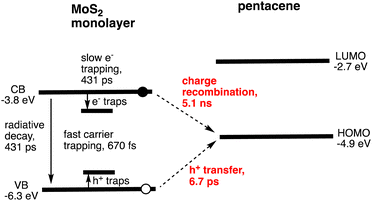
Photoinduced CS has been observed at noncovalent heterojunctions between organic small molecules and few-layer TMDs using time-resolved transient absorption (TA) and photoemission spectroscopies.20–25 Owing to the facile preparation of high-quality few-layer TMDs, most research has focused on semiconducting MoS2 and WS2. For instance, Hersam and coworkers reported ultrafast exciton dissociation and relatively long-lived CS in a heterojunction between pentacene and MoS2.21 In the experiment, a homogeneous ML-MoS2 film was grown directly on quartz wafers by CVD. Subsequently, a 30 nm thick pentacene film was deposited on the ML-MoS2. The TA spectra of the heterojunction were recorded at an excitation wavelength of 535 nm, where the excitation ratio of MoS2![[thin space (1/6-em)]](https://www.rsc.org/images/entities/char_2009.gif) :
:![[thin space (1/6-em)]](https://www.rsc.org/images/entities/char_2009.gif) pentance is 1
pentance is 1![[thin space (1/6-em)]](https://www.rsc.org/images/entities/char_2009.gif) :
:![[thin space (1/6-em)]](https://www.rsc.org/images/entities/char_2009.gif) 3. The four time constants for the decay of the MoS2 B-exciton, monitored at 612 nm, were attributed to the trapping of electrons and holes to surface defects26–28 (670 fs, 48%), hole transfer from photoexcited n-type MoS2 to p-type pentacene (6.7 ps, 28%), radiative recombination and electron trapping26,29–32 (431 ps, 9%), and charge recombination (CR) (5.1 ns, 15%) (Fig. 1 and Table 2). Interestingly, other heterojunctions also reveal similar CT (1–10 ps) and CR (1–10 ns).20–25
3. The four time constants for the decay of the MoS2 B-exciton, monitored at 612 nm, were attributed to the trapping of electrons and holes to surface defects26–28 (670 fs, 48%), hole transfer from photoexcited n-type MoS2 to p-type pentacene (6.7 ps, 28%), radiative recombination and electron trapping26,29–32 (431 ps, 9%), and charge recombination (CR) (5.1 ns, 15%) (Fig. 1 and Table 2). Interestingly, other heterojunctions also reveal similar CT (1–10 ps) and CR (1–10 ns).20–25
| Hetero-junction | τ 1 (A1) | τ 2 (A2) | τ 3 (A3) | τ 4 (A4) | τ 5 (A5) | τ 6 | Ref. |
|---|---|---|---|---|---|---|---|
| a The quantities in parenthesis are the fractional amplitudes of each component. b Poly[[4,8-bis[(2-ethylhexyl)oxy]benzo[1,2-b:4,5-b′]dithiophene-2,6-diyl][3-fluoro-2-[(2-ethylhexyl)carbonyl]-thieno[3,4-b]thiophenediyl]]. | |||||||
| Process | Carrier trapping | CT formation | Non-radiative decay | Radiative decay and e− trapping | CR | CD | |
| ML-MoS2/pentacene | 670 fs (48%) | 6.7 ps (28%) | — | 431 ps (9%) | 5.1 ns (15%) | — | 21 |
| ML-MoS2 | 670 fs (47%) | — | 16 ps (35%) | 431 ps (18%) | — | — | 21 |
| ML-MoS2/PTB7b | — | 1–5 ps (–) | — | — | 3–4 ns | — | 23 |
| ML-MoS2/ZnPc | — | 40 fs (∼100%), 120 fs | — | — | 100–1000 ps | 10 ps | 25 |
| Bulk-MoS2/ZnPc | — | Limited ED and CT | — | — | T1 formation & CR (1–100 ps) | — | 22 |
| ML-WS2/tetracene | — | 2–3 ps | — | — | 2 ns | — | 24 |
| MoS2/P3HT:[60]PCBM | — | <100 fs (from MoS2 to P3HT) | — | — | — | — | 20 |
The overall hole transfer yield (charge-transfer (CT) efficiency) was estimated to be approximately 50%, which is limited by the fast trapping process. Therefore, trap sites caused by defects in MoS2 must be minimized during preparation. The CR lifetime is also shorter than that in polymer/fullerene bulk heterojunction solar cells (20 ns to 10 μs),33 but it is longer than the lifetime of indirect excitons in planar p–n 2D–2D heterojunctions.34 This fast CR eventually limits the ability of charge carriers to diffuse to respective electrodes, thereby limiting charge collection (CC) efficiency in a solar cell. Since ML-MoS2 exhibits fast carrier trapping occurring within less than 1 ps, high light-harvesting (LH) properties of organic small molecules with a long-lived S1 state relative to MoS2 are desirable for efficient CS. Namely, exclusive LH by organic molecules leads to better light energy conversion (vide infra).
Chan and coworkers presented photoinduced charge generation at the zinc phthalocyanine (ZnPc)/MoS2 interface.22,25 They selectively excited ZnPc at 700 nm to probe the formation and decay of exciton and CT states. It was found that a large band bending in ZnPc on bulk-MoS2 limits the extent of exciton delocalization and inhibits electron injection to the conduction band (CB) of bulk-MoS2, whereas efficient exciton diffusion (ED) and CT occurs at the ML-MoS2/ZnPc interface with the small band bending in ZnPc (Fig. 2 and Table 2). Namely, a hot CT state is formed with a high efficiency (∼100%) and a lifetime of 40 fs, which is transformed into a relaxed, localized CT state with a lifetime of 120 fs. They also proposed that large band bending in ZnPc on bulk MoS2 traps the hole of the CT excited state. The hole trapping with the faster spin conversion rate in bulk-MoS2 results in the T1 formation and subsequent CR from bulk-MoS2 to ZnPc. In contrast, the time for the dissociation of the CT excited state at the ML-MoS2/ZnP is relatively fast (∼10 ps), which is explained by a large number of loosely bound CT excited states with small binding energies and large spatial delocalization. In other words, ML-MoS2 is better than bulk-MoS2 in terms of ED, CT, CD, and CC. Therefore, a combination of ML-2D materials and highly LH organic molecules is promising for optoelectronics applications.
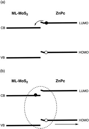 | ||
| Fig. 2 Schematic of (a) charge-transfer (CT) and (b) charge dissociation (CD) in the ML-MoS2/ZnPc heterojunction with small band bending in ZnPc. | ||
For photoelectrochemical devices with a macroscopic size of working electrodes (≥0.4 cm2) under the three electrodes configuration, there are limited examples of heterojunctions comprised of 2D layered materials and organic small molecules. In this regard, hybrids of fullerenes and 2D materials have attracted attention for the creation of novel functional materials through hybridization.35,36 Imahori and coworkers introduced composite films composed of C60 and well-exfoliated nanosheets of TMD, specifically MoS2 or WS2, obtained from the corresponding bulk materials.37 These films were conveniently fabricated onto a semiconducting SnO2 electrode using a two-step method. The first step involved the formation of aggregates by injecting a poor solvent (acetonitrile) into a good solvent (N-methyl-2-pyrrolidone (NMP)) that contained C60 and either MoS2 or WS2. The second step was the electrophoretic deposition, which was achieved by applying a direct current voltage to the aggregate solution.
The composite structures were meticulously characterized by dynamic light scattering and microscopic measurements, confirming the formation of a heterojunction between C60 and either MoS2 or WS2, with an average thickness of three layers. Upon photoexcitation of the composites on the SnO2 semiconducting electrode, they displayed significantly enhanced flash-photolysis time-resolved transient conductivities (FP-TRMCs) compared to the individual components of TMDs or C60. This indicates that the heterojunction nanostructure of TMD and C60 facilitated CS. Moreover, the decoration of TMD nanosheets with C60 molecules hindered the undesirable CR between an electron in the electrode and a hole in the TMD nanosheets. Thanks to the accelerated CS and suppressed CR, the photoelectrochemical devices with SnO2/(MoS2 + C60)m and SnO2/(WS2 + C60)m electrodes achieved incident photon-to-current efficiencies (IPCEs) of 35% and 23% at 400 nm, respectively (Table 3). These efficiencies are superior to those of the individual component films (7–13%), and the IPCE of 35% is the highest ever reported for photoelectrochemical devices under three electrodes configuration among composites of 2D layered materials and organic small molecules on semiconducting electrodes.37 As depicted in Fig. 3, the photoinduced CS and subsequent electron transfer (ET) at the heterojunctions contribute to the generation of photocurrent.
| System | Layer number | IPCE (wavelength) | TRMC (lifetime, %) | Ref. |
|---|---|---|---|---|
| SnO2/(MoS2 + C60)m | 3 | 35% (400 nm) | 1.7 × 10⁻³ cm2 V−1 s−1 (0.2 μs, 59%; 7.0 μs, 16%; 270 μs, 25%) | 37 |
| SnO2/(WS2 + C60)m | 3 | 23% (400 nm) | 1.8 × 10⁻³ cm2 V−1 s−1 (0.4 μs, 28%; 7.0 μs, 11%; 300 μs, 61%) | 37 |
| SnO2/(Sb + C60)m | 8 | 11.4% (400 nm) | 3.3 × 10⁻⁴ cm2 V−1 s−1 (7.9 μs, 33%; 410 μs, 67%) | 38 |
| (Bi + C60)m | 3 | — | No signal | 39 |
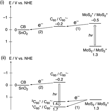 | ||
| Fig. 3 Photoinduced ET pathways in SnO2/(MoS2 + C60)m. The number of parenthesis denotes the order of the pathways. | ||
The device featuring the MoS2/C60 heterojunction demonstrated a higher IPCE compared to the device with the WS2/C60 heterojunction. Given that the TRMC values of SnO2/(MoS2 + C60)m (1.7 × 10⁻³ cm2 V−1 s−1) and SnO2/(WS2 + C60)m (1.8 × 10⁻³ cm2 V−1 s−1) are comparable, the difference could be due to the inhomogeneous film structure of the latter, which results from the strong interaction between WS2 and C60. The insights gained from these findings will offer valuable information on the photodynamics of TMD–organic nanohybrids. Consequently, this will aid in the rational design of organic–inorganic hybrid devices.
Black phosphorous (BP) is a 2D material exhibiting both high carrier mobility and a tunable direct bandgap.40 However, its high sensitivity to light, water, and oxygen limits its applications. Sb, an exfoliated 2D material obtained from bulk antimony, is considered a potential alternative for BP because of its superior stability.41,42 Imahori and coworkers focused on several-layered Sb (approximately 8 layers), which was noncovalently functionalized with C60 molecules by swiftly adding a poor solvent (acetonitrile) into a mixed dispersion of several-layered Sb and C60 in a good solvent (toluene).38 The aggregation behavior of the mixed dispersion of several-layered Sb and C60 in toluene/acetonitrile was examined by UV-visible absorption, dynamic light scattering, and microscopic measurements. These measurements confirmed the formation of the several-layered Sb–C60 composite, (Sb + C60)m, where the Sb surface is covered with C60 molecules. In a FP-TRMC measurement, (Sb + C60)m exhibited a rapid increase in transient conductivity, whereas no signals were detected in FP-TRMC measurements of the individual components, several-layered Sb and C60. This demonstrates the occurrence of photoinduced CS between the several-layer Sb and C60 in (Sb + C60)m. Moreover, a photoelectrochemical device with a SnO2/(Sb + C60)m electrode displayed an enhanced IPCE of 11.4% at 400 nm, which is higher than those of the individual components, either several-layered Sb (8.1%) or C60 (6.9%). This result can be attributed to the photoinduced CS between several-layered Sb and C60 (Fig. 4). The photoelectrochemical properties of the several-layered (Sb + C60)m are lower than those of the corresponding SnO2/(MoS2 + C60)m and SnO2/(WS2 + C60)m probably due to the poor semiconducting properties of Sb with multi-layered structures, as seen in the TRMC data (3.3 × 10⁻⁴ cm2 V−1 s−1). Nevertheless, this work represented the initial step toward the fabrication of antimonene–organic molecule heterojunctions for their application in optoelectronics.
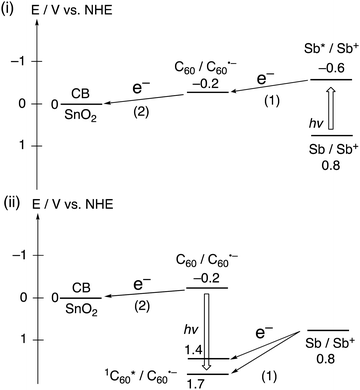 | ||
| Fig. 4 Photoinduced ET pathways in SnO2/(Sb + C60)m. The number of parenthesis denotes the order of the pathways. | ||
Bi, an exfoliated 2D material obtained from bulk bismuth, has attracted great deal of attention because of its unique electronic and spintronic properties.43 Imahori and coworkers reported few-layered Bi with an average thickness of 1.0 nm (3 layers in average), which was prepared via a successive ball mill and sonication method.39 They also hybridized Bi with C60 molecules by injecting acetonitrile into the mixed dispersion of Bi and C60 in toluene. In the FP-TRMC measurement, the few-layered Bi–C60 composite, (Bi + C60)m, showed no transient conductivity. This is in sharp contrast to the significant transient conductivity observed in the composite of Sb and C60. The energy level of the Bi oxidative excited state (−0.6 V vs. NHE) is higher than the LUMO level of C60 (−0.2 V vs. NHE) and the energy level of the Bi oxidation state (0.8 V vs. NHE) is higher than those of the C60 excited triplet (1.4 V vs. NHE) and singlet (1.7 V vs. NHE) states. Despite the energetically favorable ET processes, they were found to be inefficient. The reason for no occurrence of ET is currently unclear, but the inferior semiconducting properties of few-layered Bi, as seen in the TRMC data, may be responsible for the absence of photoinduced CS at the heterojunction. So far there is no systematic investigation on the relationship between defect sites in 2D layered materials and photophysical and photoelectrochemical properties.
Covalent approach
Although the noncovalent approach is straightforward and practical, the fundamental aspect of photoinduced CS at the heterojunction remains elusive. This is due to the amorphous nature of organic layers, which consist of inhomogeneous, numerous molecules on few-layered 2D materials. To address this issue, the covalent approach serves as a powerful method for controlling the interaction between the organic and inorganic materials through a covalent linkage at a single molecular level (Table 1). So far, such covalent functionalization has been reported for only MoS2 and WS2 with two types of approaches: (i) the utilization of preferential edge defect sites (e.g., edge defects of S atoms in MoS2), and (ii) the formation of covalent bonds on all surfaces (e.g., S–C and S–Mo bond formations in MoS2).44,45Regarding the use of TMD chalcogen vacancies at edge sites, thiol derivatives have been functionalized. In particular, 1,2-dithiolanes have proved to be useful for covalent functionalization. Tagmatarchis and coworkers created a number of TMDs that were covalently functionalized with organic electron donors or acceptors using 1,2-dithiolanes.44,45 For instance, they reported the covalent functionalization of exfoliated semiconducting MoS2 which on average had 6 layers, by a 1,2-dithiolane bearing an alkyl chain terminated with a 1-pyrenebutoxy ester (Fig. 5).46 The MoS2-based nanohybrids were characterized by spectroscopic, thermal and microscopic methods. Density functional theoretical studies, together with X-ray photoelectron spectroscopy (XPS) analysis, indicated preferential edge functionalization, primarily via sulfur addition along partially sulfur saturated zig-zag MoS2 molybdenum-edges. Before functionalization, the S 2p signal showed the major pair of peaks at 163.4 and 162.2 eV, assigned to the intact MoS2, with the minor one at 163.1 and 161.9 eV, derived from “vacancy” or damaged sites. After functionalization, these minor peaks disappeared as all the edges became fully sulfur-saturated. At the same time, there was no significant change in the Mo 3d signal. The functionalization ratio was estimated to be one per every 24 MoS2 units by thermogravimetric analysis (TGA). This rather low value is consistent with the selective edge-functionalization together with the multi-layered MoS2.
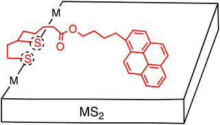 | ||
| Fig. 5 Schematic of several-layered MS2 (M = Mo or W) sheets covalently functionalized with pyrene molecules. Dotted circles denote defect sites at the edge. | ||
The UV-Vis spectrum of the MoS2–pyrene hybrid in DMF exhibited the characteristic features arising from the semiconducting MoS2 and pyrene moieties. The fluorescence spectrum of the MoS2–pyrene hybrid showed moderate 50% quenching of the pyrene fluorescence and the appearance of a broad emission at 490 nm. The authors suggested the occurrence of photoinduced energy transfer (EnT) or ET from the pyrene excited singlet state to the MoS2, but no convincing experimental evidence was given. Later, they also observed a similar photoluminescence spectrum of WS2–pyrene hybrid using the same pyrene derivative.47 At that time, the authors indicated the formation of a pyrene excimer that emits at 490 nm. Their calculations also predicted that the pyrene is stacked preferentially parallel to the MoS2 basal plane with the help of intermolecular interactions. Therefore, the emission at 490 nm might be interpreted as the CT emission arising from the CT excited state between the TMD and pyrene, as reported very recently by Imahori and coworkers (vide infra).48 In such a case, some fractions of the pyrene moieties would not interact with the MoS2 basal plane, leading to no quenching of the pyrene excited singlet state by the MoS2 because of the edge functionalization of the MoS2. This is consistent with the moderate quenching of the pyrene fluorescence and the appearance of a broad CT emission.
Tagmatarchis and coworkers extended this approach to develop a MoS2–ZnPc hybrid. Specifically, ZnPc with a 1,2-dithiolane oxide linker was used to functionalize MoS2 at defect sites located at the edges (Fig. 6).49 The structure of MoS2–ZnPc was assessed by spectroscopic, thermal, and microscopic methods, but XPS analysis was not conducted to support the covalent functionalization. The functionalization ratio was estimated to be very low (one per every 103 MoS2 units by TGA). There is no information on the number of the exfoliated MoS2, but the transmission electron microscope (TEM) image indicates the multi-layered structures. An energy-level diagram showing different photochemical events in MoS2–ZnPc was presented, indicating the occurrence of photoinduced ET to generate the MoS2˙−–ZnPc˙+ state. The photodynamic behaviors obtained by femtosecond TA spectroscopy were complicated by the involvement of continuously relaxing MoS2 excitons, making it difficult to give reliable assignment and their time constants for transient species. Nevertheless, the authors claimed to detect fingerprint of the ZnPc radical cation at 840 nm, indicating the occurrence of photoinduced CS.
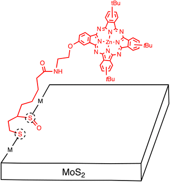 | ||
| Fig. 6 Schematic of multi-layered MoS2 sheets covalently functionalized with zincphthalocyanine (ZnPc) molecules. Dotted circles denote defect sites. | ||
This result is in sharp contrast with the covalently linked MoS2-free base porphyrin (H2P) hybrid, where the first EnT occurs from the H2P excited singlet state to the MoS2, followed by the second EnT from the MoS2 excited state to the H2P, without generating the charge-separated state.50 It is noteworthy that photoinduced CS with a time constant of 80 fs and subsequent CR with a time constant of 1–100 ps to generate the ZnPc triplet excited state was also observed for the heterojunction between bulk, single crystal MoS2 and face-on oriented, few-layered ZnPc (vide supra).22,25 The corresponding monolayer MoS2/ZnPc interface exhibited sub-100 fs CT from the ZnPc excited singlet state to the MoS2, followed by the dissociation to an electron–hole pair. The difference in the single crystal MoS2 and the monolayer MoS2 was rationalized by the different amount of band bending. The small band bending in ZnPc on monolayer MoS2 can widen the spatial range of the coherent CT and facilitate the dissociation. This emphasizes the importance of the interfacial energy level alignment at the heterojunctions between 2D layered materials and small organic molecules.
Tagmatarchis and coworkers reported the covalent functionalization of MoS2 with an electron-acceptor, perylenediimide (PDI), which possesses a 1,2-dithiolane oxidized at each sulfur atom with a 60![[thin space (1/6-em)]](https://www.rsc.org/images/entities/char_2009.gif) :
:![[thin space (1/6-em)]](https://www.rsc.org/images/entities/char_2009.gif) 40 ratio (Fig. 7).51 The MoS2–PDI hybrid structure underwent evaluation using spectroscopic, thermal, and microscopic methods. XPS analysis was not conducted to verify the covalent functionalization. The functionalization ratio was estimated to be one per every 97 MoS2 units by TGA. The average number of the exfoliated MoS2 layer was calculated to be 3–5 by analysing average heights using AFM. The photophysical relaxation of MoS2–PDI was visualized in an energy-level diagram, revealing the possibility of photoinduced CS leading to formation of the MoS2˙+–PDI˙− state. Additionally, femtosecond TA studies were performed on the MoS2–PDI hybrid in DMF. The spectral features of 1PDI*, MoS2*, and PDI are similar, and there is no selective excitation for the two moieties, making the assignment of the transient species difficult. However, the decay associated spectra exhibited three components: τ1 = 1.69 ps, assigned to the PDI and MoS2 excited states, τ2 = 2.36 ns, characterized by a peak of PDI˙− at 730 nm, and τ3 = 5.37 ns, arising from the unmodified MoS2 excited state (Table 4). These results highlight the potential of electron acceptor-tethered MoS2 and its application in optoelectronic devices.
40 ratio (Fig. 7).51 The MoS2–PDI hybrid structure underwent evaluation using spectroscopic, thermal, and microscopic methods. XPS analysis was not conducted to verify the covalent functionalization. The functionalization ratio was estimated to be one per every 97 MoS2 units by TGA. The average number of the exfoliated MoS2 layer was calculated to be 3–5 by analysing average heights using AFM. The photophysical relaxation of MoS2–PDI was visualized in an energy-level diagram, revealing the possibility of photoinduced CS leading to formation of the MoS2˙+–PDI˙− state. Additionally, femtosecond TA studies were performed on the MoS2–PDI hybrid in DMF. The spectral features of 1PDI*, MoS2*, and PDI are similar, and there is no selective excitation for the two moieties, making the assignment of the transient species difficult. However, the decay associated spectra exhibited three components: τ1 = 1.69 ps, assigned to the PDI and MoS2 excited states, τ2 = 2.36 ns, characterized by a peak of PDI˙− at 730 nm, and τ3 = 5.37 ns, arising from the unmodified MoS2 excited state (Table 4). These results highlight the potential of electron acceptor-tethered MoS2 and its application in optoelectronic devices.
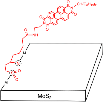 | ||
| Fig. 7 Schematic of several-layered MoS2 sheets covalently functionalized with perylenediimide (PDI) molecules. Dotted circles denote defect sites. | ||
The covalently-linked hybrids described so far possess a flexible linker between organic molecules and few-layered 2D materials, making it difficult to analyze the photodynamics due to multiple conformers arising from the flexibility and continuous relaxation of the MoS2 excited states. Furthermore, the use of defect sites in TMDs also limits the degree of functionalization on TMDs significantly, inhibiting selective excitation of organic molecules against MoS2.20–25 However, the poor reactivity at the surface of 2D layered materials has inhibited the covalent modification by organic molecules with a well-defined structure. Imahori and colleagues rationally designed a heterointerface between a photoactive molecule (i.e., pyrene, Py) and a semiconducting 2D inorganic monolayer (MoS2) with a well-defined bridge at the nanoscale (MoS2–Py). Py and MoS2 are linked by a short, semi-rigid bridge, N-benzylsuccinimide (BSI) (Fig. 8).48
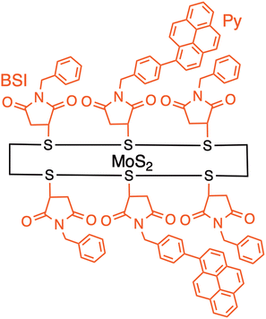 | ||
| Fig. 8 Schematic of MoS2Py hybrid where a pyrene (Py) is linked to a semiconducting 2D inorganic monolayer (MoS2) with a well-defined bridge N-benzylsuccinimide (BSI). | ||
The BSI groups can be covalently bonded onto the MoS2 surface at high densities by the reaction with N-benzylmaleimide (BMI) according to the report by Pérez and coworkers.52,53 Namely, the entire MoS2 surface is completely covered with the BSI moieties covalently. Because of the densely filled BSI moieties on MoS2, the attached Py moieties are significantly inclined toward the BSI-modified MoS2 and are in direct contact with the BSI moieties at a separation distance of approximately 1 nm. This is different from the sparse edge functionalization by Tagmatarchis and coworkers.44–47,49–51 The Py moiety is tethered to the para-position of the phenyl group by Suzuki coupling after the first-step modification of the BSI moiety on MoS2. Since the modification ratio by the Suzuki coupling is low, only 30% of the BSI on MoS2 is modified with the Py moiety. The moderate efficiency of the Suzuki coupling results from the detachment of halogen atoms from the para-position of the phenyl group during the reaction.54,55 Thus, the excited singlet state of Py at the single molecular level is expected to interact solely with MoS2 to form the CT excited state (i.e., excited state with CT character) and/or the charge-separated state at the well-defined heterointerface of MoS2–Py.
The photoluminescence spectra of MoS2–Py and the pyrene reference were taken in DMF. The pyrene reference, when excited at 345 nm, showed intense emission peaks at 382 and 402 nm with an emission quantum yield of 56%. When the photoluminescence spectrum of MoS2–Py was recorded with an excitation wavelength at 345 nm, the excited singlet state of pyrene was strongly quenched, and a broad, red-shifted intense emission was observed at 453 nm. The emission decay profiles exhibited the photoluminescence lifetime of MoS2–Py (2.7 ns), which is much shorter than that of the pyrene reference (77 ns). As solvent polarity increased from toluene to DMF, MoS2–Py also revealed a gradual red-shift and decrease in emission, which can be assigned to CT emission. Surprisingly, the emission quantum yield of MoS2–Py (68% in DMF) is high, considering the emission quantum yield of typical intermolecular CT excited states between pyrene derivatives and N,N-dimethylaniline (approximately 20% in nonpolar solvents). This may originate from the short, fixed orientation between the pyrene and MoS2 through the BSI moieties on MoS2. In other words, this geometry stabilizes the CT excited state and suppresses the nonradiative decay of the CT excited state.
The picosecond TA spectroscopic measurement of MoS2–Py was conducted with an excitation wavelength at 345 nm, where the excitation ratio of MoS2 : Py is 1 : 2. Three components with lifetimes of τ1 = 0.9 ps, τ2 = 117 ps, and τ3 = 2540 ps were deduced from the global analysis. The first and second decay components, characterized by bleach arising from the excited state of MoS2, were assigned to the decay of the hot and cooled MoS2 excitons. The third component, which shows broad positive signals in the visible and NIR regions with a peak around 860 nm, is assignable to the decay of the CT excited state, which is in good agreement with the emission lifetime of MoS2–Py (2.7 ns). From the rise component at 850 nm, the CT excited state is generated with a time constant of 1.2 ps (Fig. 9 and Table 4). Considering the lifetime of the pyrene reference (77 ns), the CT efficiency from the pyrene excited singlet state to MoS2 is estimated to be ∼100%.
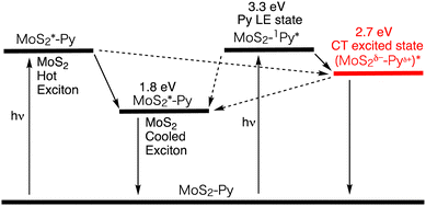 | ||
| Fig. 9 Relaxation pathways of MoS2–Py in DMF. The energy level of the CT state was determined by the peak position of the emission. The plausible pathways are shown as a black dotted arrow. | ||
Theoretical studies were also conducted for the MoS2–Py model with a Mo28S63 nanosheet, in which one Py–BSI and two BSI units are covalently attached to sulfur atoms. The geometry optimization of the Py–MoS2 model revealed the geometry of the Py moiety on MoS2 that is similar to Fig. 8, which aligns well with the small thickness (2.6 nm) of the experimentally obtained monolayer MoS2–Py using AFM. Furthermore, the time-dependent density functional theory (TDDFT) and the three-dimensional reference interaction site model (3D-RISM) were used to investigate the emission behavior of MoS2–Py. The LUMO of the Py moiety is hybridized with the vacant orbitals of MoS2, signifying the formation of the CT excited state by interaction between the vacant orbitals of MoS2 and the excited state of pyrene. Specifically, photoexcitation of the Py moiety in the MoS2–Py covalently linked system effectively formed the long-lived, highly emissive CT excited state, delocalizing over the heterointerface of pyrene and monolayered MoS2. The highly emissive CT excited state may provide insight into how to reduce the voltage loss stemming from nonradiative CR in organic solar cells (OSCs). As has been suggested by several groups,56–60 if the CT excited state becomes more emissive after hybridizing between the locally-excited (LE) and CT excited states due to the small offset for the CT formation, nonradiative vibrational CR would be inhibited, reducing the voltage loss. Such CT states would be transformed into charge-separated states by either attaching an additional donor moiety to the pyrene or weakening electronic coupling between the pyrene and MoS2. Accordingly, this study provides a fundamental understanding of interactions in the excited states at heterojunctions between 2D monolayered materials and single organic molecules. This will be useful for the applications of organic–inorganic 2D heterointerfaces in optoelectronic devices and sensors. However, exfoliation and chemical modification may increase defect sites in TMDs, deteriorating their intrinsic photophysical properties. The effects of defect sites in 2D layered materials need to be examined systematically for better understanding of photodynamics at the heterojunctions.
Several researchers have observed photocurrent generation at covalently-linked heterojunctions between 2D materials and organic molecules, but the detailed mechanism has not been addressed because of the use of flexible bridges.61–63
Applications
Potential applications of p–n heterojunctions between small organic molecules and 2D layered materials include photodetectors, photocatalysts, solar cells, and photoelectrochemical devices. In particular, there are a number of TMC-organic small molecule heterojunction photodetectors (Table 5).64–78 TMDs such as MoS2, BiSe3, BiTe3, MoSe2, WS2, and InSe have been combined with organic molecules to fabricate photo-transistors and diodes. All devices utilize ML-2D TMCs with suitable band alignment of organic molecule layers, forming a type-II heterojunctions. Remarkably, the MoS2/BTBT transistor exhibited an excellent photoresponsivity of 475 A W−1, enhanced external quantum efficiency of 1.45 × 10⁵%, and a high on/off ratio,64 demonstrating the utility of TMC-organic small molecule heterojunctions as optoelectronic devices.| Heteojunction | Type | Detection range | Responsivity | Response speed | Ref. |
|---|---|---|---|---|---|
| a BTBT: (12-(benzo[b]benzo[4,5]thieno[2,3-d]thiophen-2-yl)dodecyl)-phosphonic acid. b PDVT-10: poly{3,6-dithiophen-2-yl-2,5-di(2-decyltetradecyl)}-pyrrolo[3,4-c]pyrrole-1,4-dione-alt-thienylenevin. c PDPP3T: poly[[2,5-bis(2-hexyldecyl)-2,3,5,6-tetrahydro-3,6-dioxo-pyrrolo[3,4-c]pyrrole-1,4-diyl][2,2′:5′,2′′-terthiophene]-5,5′′-diyl]. d PTCDA: perylenetetracarboxylic dianhydride. | |||||
| MoS2/BTBTa | Transistor | 406 nm | 475 A W−1 | 5.5–17.8 s | 64 |
| MoS2/ZnPc | Transistor | 532 nm | 430 A W−1 | 8–72 ms | 65 |
| MoS2/CuPc | Transistor | 520 nm | 1.98 A W−1 | 0.3 s | 66 |
| MoS2/PDVT-10b | Transistor | White light | 1.38 A W−1 | — | 67 |
| MoS2/rhodamine 6G | Transistor | 520 nm | 1.17 A W−1 | — | 68 |
| MoS2/rubrene | Diode | 532 nm | 0.5 A W−1 | <5 ms | 69 |
| MoS2/PDPP3Tc | Transistor | 660 nm | 0.45 A W−1 | 4–40 ms | 70 |
| MoS2/C8-BTBT | Diode | White light | 22 mA W−1 | — | 71 |
| MoS2/rubrene | Transistor | 532 nm | 0.8 mA W−1 | — | 72 |
| MoS2/pentacene | Diode | 532 nm | — | 1.8–2 ms | 73 |
| MoSe2/NiPC | Diode | 658 nm | 5.95 A W−1 | — | 74 |
| WS2/PTCDAd | Diode | 430 nm | — | — | 75 |
| InSe/C8-BTBT | Diode | 532 nm | — | — | 76 |
| Bi2Se3/rubrene | Transistor | 532 nm | 124 A W−1 | 10–59 ms | 77 |
| Bi2Te3/pentacene | Diode | 450–3500 nm | 14.89 A W−1 | 2.98–3.57 ms | 78 |
Another issue to be addressed is their layered-number dependent properties at the heterojunctions. However, conventional approaches need multiple complicated preparation procedures to fabricate the heterojunctions. Choi and coworkers developed a series of heterojunctions from eosin Y (EY) molecules stacked on mechanically exfoliated WSe2 flakes of ML through 6-layer (6L) via one-step solution phase chemistry.79 As the layer number of WSe2 increases, its CB level decreases from –3.70 eV and VB level increases from −5.35 eV. EY's LUMO level (−4.05 eV) is lower than the CB of 6L WSe2 and its HOMO level (−4.75 eV) is higher than the VB of ML WSe2, forming a type-II band alignment. When the WSe2 was excited, the WSe2/EY heterojunction showed significantly enhanced photoconductivity compared to pristine WSe2 with a lower barrier height and a longer effective screening length. As the layer-number increased, the photoresponse decreased gradually and finally increased slightly. Overall, the staggered bands between the EY layer and ML-WSe2 flake can facilitate the exciton dissociation efficiently, leading to enhanced photoconductivity. This is consistent with the results on ML-MoS2/ZnP.22,25
Conclusions and perspectives
We have shown that p–n heterojunctions between small organic molecules and 2D layered materials are useful for photoinduced CS and photocurrent generation. The noncovalent approach is facile and practical for fabrication, although typically only limited information is available for the close relationship between the structure and photophysical and photoelectrochemical properties due to its amorphous nature. Meanwhile, covalent approach is powerful, but tedious and time-consuming for the preparation. Moreover, edge functionalization with flexible bridge leads to the formation of multiple conformations, making it difficult to analyze the photodynamics. On the other hand, surface functionalization with rigid bridge results in well-defined geometry, but it is synthetically challenging due to the poor surface reactivity of few-layered 2D materials in addition to the defect formation by exfoliation and chemical reactions. Other types of exfoliation and covalent modification under mild conditions need to be exploited for the well-defined covalent heterojunction hybrids without damaging their electronic structures.80Unexplored potential applications of p–n heterojunctions between small organic molecules and 2D layered materials include photocatalysts and solar cells. So far, a combination of 2D layered materials with inorganic materials has been investigated for the applications. For photocatalysts, improving the CS efficiency and lifetime is essential. The charge-separated state must be quenched efficiently by diffusing reagents in solutions.81,82 For solar cells, such p–n heterojunctions have not been used at this stage because of insufficient photovoltaic parameters for achieving high IPCE values. ML-2D layered materials are potential candidates, as seen in ML-MoS2/ZnP heterojunction.22,25 We need to develop organic molecules with an excellent light-harvesting property in visible and near-infra red regions, long-lived excited state (e.g., long exciton diffusion length),83,84 and self-CT and CD without bulk heterojuctions,59 as demonstrated in non-fullerene acceptors.
HOMO and LUMO of organic small molecules can be tuned to make a desirable heterojunction with 2D layered materials. If we can modulate the electronic coupling at the p–n heterointerface intentionally, efficient formation of CT excited states and subsequent charge dissociation at the interface for optoelectronics and solar cells will be achieved.
Author contributions
H. I. and M. A. researched and wrote the initial manuscript. All authors contributed to editing and finalizing the manuscript. Hiroshi Imahori: conceptualizing (lead); writing – original draft, review & editing (equal). Midori Akiyama: writing – original draft, review & editing (equal).Data availability
Data sharing is not applicable to this article as no datasets were generated or analysed during the current study.Conflicts of interest
There are no conflicts to declare.Acknowledgements
We would like to express our gratitude to the dedicated contributions of coworkers and students who participated in the team-based collaboration mentioned in this review. We wish to convey our appreciation for Transformative Research Areas (A), “Dynamic Exciton: Emerging Science and Innovation (20A201)” (JSPS KAKENHI Grant Numbers JP20H05831 (H. I.), JP20H05832 (H. I.), JP21H05385 (M. A.), and JP23H03950 (M. A.)) and Grant-in-Aid for Scientific Research (A) (JSPS KAKENHI Grant Numbers JP23H00309 (H. I.)).References
- M. Buscema, D. J. Groenendijk, G. A. Steele, H. S. J. van der Zant and A. Castellanos-Gomez, Nat. Commun., 2014, 5, 4651 CrossRef CAS.
- Y. Taniyasu, M. Kasu and T. Makimoto, Nature, 2006, 441, 325 CrossRef CAS.
- V. M. Agranovich, Y. N. Gartstein and M. Litinskaya, Chem. Rev., 2011, 111, 5179 CrossRef CAS.
- R. Otero, A. L. Vázquez de Parga and J. M. Gallego, Surf. Sci. Rep., 2017, 72, 105 CrossRef CAS.
- H. Jin, J. Li, J. Iocozzia, X. Zeng, P.-C. Wei, C. Yang, N. Li, Z. Liu, J. H. He, T. Zhu, J. Wang, Z. Lin and S. Wang, Angew. Chem., Int. Ed., 2019, 58, 15206 CrossRef CAS.
- C. Zang, M. Xu, L. Zhang, S. Liu and W. Xie, J. Mater. Chem. C, 2021, 9, 1484 RSC.
- K. S. Novoselov, D. Jiang, F. Schedin, T. J. Booth, V. V. Khotkevich, S. V. Morozov and A. K. Geim, Proc. Natl. Acad. Sci. U. S. A., 2005, 102, 10451 CrossRef CAS.
- Q. H. Wang, K. Kalantar-Zadeh, A. Kis, J. N. Coleman and M. S. Strano, Nat. Nanotechnol., 2012, 7, 699 CrossRef CAS PubMed.
- C. Tan, X. Cao, X.-J. Wu, Q. He, J. Yang, X. Zhang, J. Chen, W. Zhao, S. Han, G.-H. Nam, M. Sindoro and H. Zhang, Chem. Rev., 2017, 117, 6225 CrossRef CAS PubMed.
- G. R. Bhimanapati, Z. Lin, V. Meunier, Y. Jung, J. Cha, S. Das, D. Xiao, Y. Son, M. S. Strano, V. R. Cooper, L. Liang, S. G. Louie, E. Ringe, W. Zhou, S. S. Kim, R. R. Naik, B. G. Sumpter, H. Terrones, F. Xia, Y. Wang, J. Zhu, D. Akinwande, N. Alem, J. A. Schuller, R. E. Schaak, M. Terrones and J. A. Robinson, ACS Nano, 2015, 9, 11509 CrossRef CAS.
- W. Xia, L. Dai, P. Yu, X. Tong, W. Song, G. Zhang and Z. Wang, Nanoscale, 2017, 9, 4324 RSC.
- M. Chhowalla, H. S. Shin, G. Eda, L.-J. Li, K. P. Loh and H. Zhang, Nat. Chem., 2013, 5, 263 CrossRef PubMed.
- Y.-C. Lin, D. O. Dumcenco, Y.-S. Huang and K. Suenaga, Nat. Nanotechnol., 2014, 9, 391 CrossRef CAS PubMed.
- Y. L. Huang, Y. J. Zheng, Z. Song, D. Chi, A. T. S. Wee and S. Y. Quek, Chem. Soc. Rev., 2018, 47, 3241 RSC.
- J. Azadmanjiri, P. Kumar, V. K. Srivastava and Z. Sofer, ACS Appl. Nano Mater., 2020, 3, 3116 CrossRef CAS.
- B. Kirubasankar, Y. S. Won, L. A. Adofo, S. H. Choi, S. M. Kim and K. K. Kim, Chem. Sci., 2022, 13, 7707 RSC.
- S. Zhang, S. Guo, Z. Chen, Y. Wang, H. Gao, J. Gómez-Herrero, P. Ares, F. Zamora, Z. Zhu and H. Zeng, Chem. Soc. Rev., 2018, 47, 982 RSC.
- P. Vishnoi, K. Pramoda and C. N. R. Rao, ChemNanoMat, 2019, 5, 1062 CrossRef CAS.
- T. Wang, H. Wang, Z. Kou, W. Liang, X. Luo, F. Verpoort, Y.-J. Zeng and H. Zhang, Adv. Funct. Mater., 2020, 30, 2002885 CrossRef CAS.
- C. E. Petoukhoff, M. B. M. Krishna, D. Voiry, I. Bozkurt, S. Deckoff-Jones, M. Chhowalla, D. M. O’Carroll and K. M. Dani, ACS Nano, 2016, 10, 9899 CrossRef CAS PubMed.
- S. B. Homan, V. K. Sangwan, I. Balla, H. Bergeron, E. A. Weiss and M. C. Hersam, Nano Lett., 2017, 17, 164 CrossRef.
- T. R. Kafle, B. Kattel, S. D. Lane, T. Wang, H. Zhao and W.-L. Chan, ACS Nano, 2017, 11, 10184 CrossRef CAS.
- C. Zhong, V. K. Sangwan, C. Wang, H. Bergeron, M. C. Hersam and E. A. Weiss, J. Phys. Chem. Lett., 2018, 9, 2484 CrossRef CAS PubMed.
- T. Zhu, L. Yuan, Y. Zhao, M. Zhou, Y. Wan, J. Mei and L. Huang, Sci. Adv., 2018, 4, eaao3104 CrossRef PubMed.
- T. R. Kafle, B. Kattel, P. Yao, P. Zereshki, H. Zhao and W.-L. Chan, J. Am. Chem. Soc., 2019, 141, 11328 CrossRef CAS.
- S. H. Aleithan, M. Y. Livshits, S. Khadka, J. J. Rack, M. E. Kordesch and E. Stinaff, Phys. Rev. B, 2016, 94, 035445 CrossRef.
- P. D. Cunningham, K. M. McCreary, A. T. Hanbicki, M. Currie, B. T. Jonker and L. M. Hayden, J. Phys. Chem. C, 2016, 120, 5819 CrossRef CAS.
- H. Wang, C. Zhang and F. Rana, Nano Lett., 2015, 15, 339 CrossRef CAS PubMed.
- H. Shi, R. Yan, S. Bertolazzi, J. Brivio, B. Gao, A. Kis, D. Jena, H. G. Xing and L. Huang, ACS Nano, 2013, 7, 1072 CrossRef CAS PubMed.
- M. Palummo, M. Bernardi and J. C. Grossman, Nano Lett., 2015, 15, 2794 CrossRef CAS PubMed.
- O. Salehzadeh, N. H. Tran, X. Liu, I. Shih and Z. Mi, Nano Lett., 2014, 14, 4125 CrossRef CAS PubMed.
- M. Amani, D.-H. Lien, D. Kiriya, J. Xiao, A. Azcatl, J. Noh, S. R. Madhvapathy, R. Addou, S. KC, M. Dubey, K. Cho, R. M. Wallace, S.-C. Lee, J.-H. He, J. W. Ager III, X. Zhang, E. Yablonovitch and A. Javey, Science, 2015, 350, 1065 CrossRef CAS PubMed.
- I. Montanari, A. F. Nogueira, J. Nelson, J. R. Durrant, C. Winder, M. A. Loi, N. S. Sariciftci and C. Brabec, Appl. Phys. Lett., 2002, 81, 3001 CrossRef CAS.
- F. Ceballos, M. Z. Bellus, H.-Y. Chiu and H. Zhao, ACS Nano, 2014, 8, 12717 CrossRef CAS.
- M. Chen, R. Guan and S. Yang, Adv. Sci., 2019, 6, 1800491 Search PubMed.
- T. Umeyama and H. Imahori, Nanoscale Horiz., 2018, 3, 352 RSC.
- J. Baek, T. Umeyama, W. Choi, Y. Tsutsui, H. Yamada, S. Seki and H. Imahori, Chem. – Eur. J., 2018, 24, 1561 CrossRef CAS PubMed.
- T. Umeyama, T. Ohara, Y. Tsutsui, S. Nakano, S. Seki and H. Imahori, Chem. – Eur. J., 2020, 26, 6726 CrossRef CAS PubMed.
- T. Umeyama, H. Xu, T. Ohara, Y. Tsutsui, S. Seki and H. Imahori, J. Phys. Chem. C, 2021, 125, 13954 CrossRef CAS.
- Y. Abate, D. Akinwande, S. Gamage, H. Wang, M. Snure, N. Poudel and S. B. Cronin, Adv. Mater., 2018, 30, 1704749 CrossRef.
- G. Abellán, P. Ares, S. Wild, E. Nuin, C. Neiss, D. R.-S. Miguel, P. Segovia, C. Gibaja, E. G. Michel, A. Görling, F. Hauke, J. Gómez-Herrero, A. Hirsch and F. Zamora, Angew. Chem., Int. Ed., 2017, 56, 14389 CrossRef.
- Q. Xiao, C.-X. Hu, H.-R. Wu, Y.-Y. Ren, X.-Y. Li, Q.-Q. Yang, G.-H. Dun, Z.-P. Huang, Y. Peng, F. Yan, Q. Wang and H.-L. Zhang, Nanoscale Horiz., 2020, 5, 124 RSC.
- H. Huang, X. Ren, Z. Li, H. Wang, Z. Huang, H. Qiao, P. Tang, J. Zhao, W. Liang, Y. Ge, J. Liu, J. Li, X. Qi and H. Zhang, Nanotechnology, 2018, 29, 235201 CrossRef PubMed.
- A. Stergiou and N. Tagmatarchis, Chem. – Eur. J., 2018, 24, 18246 CrossRef CAS PubMed.
- C. Stangel, E. Nikoli and N. Tagmatarchis, Adv. Energy Sustainability Res., 2022, 3, 2200097 CrossRef CAS.
- R. Canton-Victoria, Y. Sayed-Ahmad-Baraza, M. Pelaez-Fernandez, R. Arenal, C. Bittencourt, C. P. Ewels and N. Tagmatarchis, npj 2D Mater. Appl., 2017, 1, 13 CrossRef.
- R. Canton-Victoria, S. Nufer, X. Che, Y. Sayed-Ahmad-Baraza, R. Arenal, C. Bittencourt, A. Brunton, A. B. Dalton, C. P. Ewels and N. Tagmatarchis, Mater. Adv., 2020, 1, 2459 RSC.
- T. Umeyama, D. Mizutani, Y. Ikeda, W. R. Osterloh, F. Yamamoto, K. Kato, A. Yamakata, M. Higashi, T. Urakami, H. Sato and H. Imahori, Chem. Sci., 2023, 14, 11914 RSC.
- R. Canton-Victoria, H. B. Gobeze, V. M. Blas-Ferrando, J. Ortiz, Y. Jang, F. Fernández-Lázaro, Á. Sastre-Santos, Y. Nakanishi, H. Shinohara, F. D’Souza and N. Tagmatarchis, Angew. Chem., Int. Ed., 2019, 58, 5712 CrossRef.
- R. Canton-Victoria, T. Scharl, A. Stergiou, A. Cadranel, R. Arenal, D. M. Guldi and N. Tagmatarchis, Angew. Chem., Int. Ed., 2020, 59, 3976 CrossRef.
- I. K. Sideri, Y. Jang, J. Garcés-Garcés, Á. Sastre-Santos, R. Canton-Victoria, R. Kitaura, F. Fernández-Lázaro, F. D’Souza and N. Tagmatarchis, Angew. Chem., Int. Ed., 2021, 60, 9120 CrossRef CAS PubMed.
- M. Vera-Hidalgo, E. Giovanelli, C. Navío and E. M. Pérez, J. Am. Chem. Soc., 2019, 141, 3767 CrossRef CAS.
- R. Quirós-Ovies, M. V. Sulleiro, M. Vera-Hidalgo, J. Prieto, I. J. Gómez, V. Sebastián, J. Santamaría and E. M. Pérez, Chem. – Eur. J., 2020, 26, 6629 CrossRef.
- T. Umeyama, J. Baek, Y. Sato, K. Suenaga, F. Abou-Chahine, N. V. Tkachenko, H. Lemmetyinen and H. Imahori, Nat. Commun., 2015, 6, 7732 CrossRef CAS PubMed.
- T. Umeyama, J. Baek, J. Mihara, N. V. Tkachenko and H. Imahori, Chem. Commun., 2017, 53, 1025 RSC.
- H. Imahori, Y. Kobori and H. Kaji, Acc. Mater. Res., 2021, 2, 501 CrossRef CAS.
- H. Imahori, Bull. Chem. Soc. Jpn., 2023, 96, 339 CrossRef CAS.
- T. Saito, S.-i Natsuda, K. Imakita, Y. Tamai and H. Ohkita, Sol. RRL, 2020, 4, 2000255 CrossRef CAS.
- A. Yamakata, K. Kato, T. Urakami, S. Tsujimura, K. Murayama, M. Higashi, H. Sato, Y. Kobori, T. Umeyama and H. Imahori, Chem. Sci., 2024, 15, 12686 RSC.
- H. Imahori and M. Akiyama, J. Chem. Phys., 2024, 161, 080901 CrossRef CAS PubMed.
- X. Chen, D. McAteer, C. McGuinness, I. Godwin, J. N. Coleman and A. R. McDonald, Chem. – Eur. J., 2018, 24, 351 CrossRef CAS.
- M. P. Minadakis, R. Canton-Victoria, C. Stangel, E. Klontzas, R. Arenal, J. Hernández-Ferrer, A. M. Benito, W. K. Maser and N. Tagmatarchis, ChemSusChem, 2023, 16, e202202322 CrossRef CAS.
- R. Canton-Victoria, T. Hotta, Y. Tanuma, I. K. Sideri, N. Tagmatarchis, C. Ewels and R. Kitaura, J. Phys. Chem. C, 2023, 127, 10699 CrossRef.
- B. Zhao, Z. Gan, M. Johnson, E. Najafidehaghani, T. Rejek, A. George, R. H. Fink, A. Turchanin and M. Halik, Adv. Funct. Mater., 2021, 31, 2105444 CrossRef CAS.
- Y. Huang, F. Zhuge, J. Hou, L. Lv, P. Luo, N. Zhou, L. Gan and T. Zhai, ACS Nano, 2018, 12, 4062 CrossRef CAS PubMed.
- J. Pak, J. Jang, K. Cho, T.-Y. Kim, J.-K. Kim, Y. Song, W.-K. Hong, M. Min, H. Lee and T. Lee, Nanoscale, 2015, 7, 18780 RSC.
- J. Yan, Y. Hao, Y. Cui, J. Zhang, Y. Zou, W. Zhang, G. Yu, J. Zheng, W. Xu and D. Zhu, J. Mater. Chem. C, 2018, 6, 12976 RSC.
- S. H. Yu, Y. Lee, S. K. Jang, J. Kang, J. Jeon, C. Lee, J. Y. Lee, H. Kim, E. Hwang, S. Lee and J. H. Cho, ACS Nano, 2014, 8, 8285 CrossRef CAS PubMed.
- F. Liu, W. L. Chow, X. He, P. Hu, S. Zheng, X. Wang, J. Zhou, Q. Fu, W. Fu, P. Yu, Q. Zeng, H. J. Fan, B. K. Tay, C. Kloc and Z. Liu, Adv. Funct. Mater., 2015, 25, 5865 CrossRef CAS.
- M. Sun, P. Yang, D. Xie, Y. Sun, J. Xu, T. Ren and Y. Zhang, Adv. Electron. Mater., 2019, 5, 1800580 CrossRef.
- D. He, Y. Pan, H. Nan, S. Gu, Z. Yang, B. Wu, X. Luo, B. Xu, Y. Zhang, Y. Li, Z. Ni, B. Wang, J. Zhu, Y. Chai, Y. Shi and X. Wang, Appl. Phys. Lett., 2015, 107, 183103 CrossRef.
- C.-J. Park, H. J. Park, J. Y. Lee, J. Kim, C.-H. Lee and J. Joo, ACS Appl. Mater. Interfaces, 2018, 10, 29848 CrossRef CAS.
- D. Jariwala, S. L. Howell, K.-S. Chen, J. Kang, V. K. Sangwan, S. A. Filippone, R. Turrisi, T. J. Marks, L. J. Lauhon and M. C. Hersam, Nano Lett., 2016, 16, 497 CrossRef CAS PubMed.
- J. Choi, H. Zhang and J. H. Choi, ACS Nano, 2016, 10, 1671 CrossRef CAS PubMed.
- X. Liu, J. Gu, K. Ding, D. Fan, X. Hu, Y.-W. Tseng, Y.-H. Lee, V. Menon and S. R. Forrest, Nano Lett., 2017, 17, 3176 CrossRef CAS PubMed.
- S. Li, C. Zhong, A. Henning, V. K. Sangwan, Q. Zhou, X. Liu, M. S. Rahn, S. A. Wells, H. Y. Park, J. Luxa, Z. Sofer, A. Facchetti, P. Darancet, T. J. Marks, L. J. Lauhon, E. A. Weiss and M. C. Hersam, ACS Nano, 2020, 14, 3509 CrossRef CAS PubMed.
- K. Pei, F. Wang, W. Han, S. Yang, K. Liu, K. Liu, H. Li and T. Zhai, Small, 2020, 16, 2002312 CrossRef CAS.
- M. Yang, J. Wang, Y. Zhao, L. He, C. Ji, X. Liu, H. Zhou, Z. Wu, X. Wang and Y. Jiang, ACS Nano, 2019, 13, 755 CrossRef CAS PubMed.
- J. Ji and J. H. Choi, Adv. Mater. Interfaces, 2019, 6, 1900637 CrossRef.
- K. C. Knirsch, N. C. Berner, H. C. Nerl, C. S. Cucinotta, Z. Gholamvand, N. McEvoy, Z. Wang, I. Abramovic, P. Vecera, M. Halik, S. Sanvito, G. S. Duesberg, V. Nicolosi, F. Hauke, A. Hirsch, J. N. Coleman and C. Backes, ACA Nano, 2015, 9, 6018 CrossRef CAS.
- S. Ibrahim, T. Pal and S. Ghosh, New J. Chem., 2019, 43, 10118 RSC.
- S. Fukuzumi, H. Imahori, K. Okamoto, H. Yamada, M. Fujitsuka, O. Ito and D. M. Guldi, J. Phys. Chem. A, 2002, 106, 1903 CrossRef CAS.
- T. Umeyama, K. Igarashi, D. Sasada, Y. Tamai, K. Ishida, T. Koganezawa, S. Ohtani, K. Tanaka, H. Ohkita and H. Imahori, Chem. Sci., 2020, 11, 3250 RSC.
- T. Umeyama, K. Igarashi, D. Sasada, K. Ishida, T. Koganezawa, S. Ohtani, K. Tanaka and H. Imahori, ACS Appl. Mater. Interfaces, 2020, 12, 39236 CrossRef CAS.
| This journal is © The Royal Society of Chemistry 2025 |

