
 Open Access Article
 This Open Access Article is licensed under a Creative Commons Attribution-Non Commercial 3.0 Unported Licence
Indoor light energy harvesting perovskite solar cells: from device physics to AI-driven strategies
Wenning
Chen†
 ac,
Kelvian T.
Mularso†
bc,
Bonghyun
Jo
*bc and
Hyun Suk
Jung
*abc
ac,
Kelvian T.
Mularso†
bc,
Bonghyun
Jo
*bc and
Hyun Suk
Jung
*abc
aDepartment of Future Energy Engineering, Sungkyunkwan University, Suwon 16419, Republic of Korea
bSchool of Advanced Materials Science and Engineering, Sungkyunkwan University, Suwon 16419, Republic of Korea
cSKKU Institute of Energy Science and Technology (SIEST), Sungkyunkwan University, Suwon 16419, Republic of Korea. E-mail: jbh0721@skku.edu; hsjung1@skku.edu
First published on 14th March 2025
Abstract
The rapid advancement of indoor perovskite solar cells (IPSCs) stems from the growing demand for sustainable energy solutions and the proliferation of internet of things (IoT) devices. With tunable bandgaps and superior light absorption properties, perovskites efficiently harvest energy from artificial light sources like LEDs and fluorescent lamps, positioning IPSCs as a promising solution for powering smart homes, sensor networks, and portable electronics. In this review, we introduce recent research that highlights advancements in material optimization under low-light conditions, such as tailoring wide-bandgap perovskites to match indoor light spectra and minimizing defects to enhance stability. Notably, our review explores the integration of artificial intelligence (AI) and machine learning (ML), which are transforming IPSC development by facilitating efficient material discovery, optimizing device architectures, and uncovering degradation mechanisms. These advancements are driving the realization of sustainable indoor energy solutions for interconnected smart technologies.
 Wenning Chen | Wenning Chen is a PhD candidate in the Department of Future Energy Engineering at Sungkyunkwan University. His current research topics are the analysis of artificial intelligence driven perovskite optoelectronic mechanisms, and the development of high-performance perovskite optoelectronic devices. |
 Kelvian T. Mularso | Kelvian T. Mularso is a PhD candidate under the supervision of Prof. Hyun Suk Jung at Advanced Materials Science and Engineering Department of Sungkyunkwan University, South Korea, specializing in perovskite solar cells. His research focuses on optimizing charge transport, power conversion efficiency, and stability in perovskite solar cells through low-dimensional materials. He has extensive experience in solution-processed thin film fabrication, material characterization techniques and optoelectronic device analysis. |
 Bonghyun Jo | Bonghyun Jo completed a PhD in Energy Science at Sungkyunkwan University in 2020. Currently he is a research professor under supervision of Prof. Hyun Suk Jung at Material science and engineering department, Sungkyunkwan University. His research is focused on the development of perovskite solar cells, and perovskite photodiode, especially machine learning-driven optimization of additives, novel compositions, and optoelectronic analysis. |
 Hyun Suk Jung | Hyun Suk Jung is a fellow professor in school of Advanced Materials Science & Engineering at Sungkyunkwan University (SKKU). He serves as director of center for future energy conversion in SKKU Institute of Energy Science & Technology (SIEST). He received his PhD in Materials Science & Engineering from Seoul National University in 2004 and joined Los Alamos National Laboratory as a director's postdoctoral fellow in 2005. He has published over 250 peer-reviewed papers and holds over 70 patents regarding synthesis of inorganic nanomaterials and solar energy conversion devices. His current H-index is 66. He presently researches perovskite optoelectronics, including flexible perovskite modules, tandem solar cells, solar cell recycling, photo-sensors and memristors. |
Wider impactOur review highlights key advancements in optimizing perovskite materials for low-light indoor environments, addressing challenges like crystallization control, defect engineering, and stability. We explore prospects for integrating indoor perovskite solar cells (IPSCs) into smart technologies such as IoT devices and emphasize the transformative role of machine learning (ML) in IPSC development. ML accelerates innovation through high-throughput screening, predictive modeling, and insights into defect states, enabling efficient bandgap tuning, novel material discovery, and adaptations for indoor light conditions. This work underscores the transition of ML strategies from outdoor to indoor solar cells, advancing sustainable energy solutions by improving energy-harvesting efficiency through computational techniques. |
1. Introduction
The escalating environmental concerns and the global push towards sustainable energy have catalyzed the rapid advancement of photovoltaic technologies, positioning perovskite solar cells (PSCs) at the forefront of solar energy application. PSCs are distinguished by their remarkable efficiency, low fabrication costs, and exceptional optoelectronic properties, such as excellent light absorption, tunable bandgaps, and long carrier diffusion lengths.1–3 These unique characteristics have made PSCs a promising candidate for diverse energy applications, particularly in low-light environments where traditional solar technologies struggle to perform effectively.As the world becomes increasingly interconnected through the internet of things (IoT), the demand for reliable, low-power energy sources to sustain trillions of sensors is accelerating. Powering billions of IoT sensors and devices solely with batteries presents significant challenges, including frequent maintenance and environmental waste, underscoring the need for alternative energy solutions like indoor photovoltaics (IPVs).4 Indoor environments impose different requirements compared to outdoor applications, requiring customized materials and designs, harnessing the energy from artificial indoor light sources such as fluorescent lamps (FL) and light-emitting diodes (LEDs) to power small electronics and sensors.5 The tunable bandgap of perovskites allows these materials to efficiently absorb the unique spectral characteristics of indoor light, setting them apart from traditional PV materials optimized for outdoor sunlight.
Nowadays, research on IPVs has focused on exploring new compositions and optimizing the structure of devices to improve their stability and efficiency under unique indoor conditions. Efforts include enhancing moisture resistance and reducing the rate of degradation in response to prolonged exposure to indoor lighting. Moreover, given the low power requirements of IoT devices, perovskite PV systems designed for indoor use are being integrated into compact energy-harvesting solutions, opening up potential markets in smart homes,6 sensor networks,7 and portable electronics.8 At the same time, efforts to reduce manufacturing costs and scale production through various printing techniques, such as roll-to-roll processing,9 inkjet printing,10 blade coating,11 and slot-die coating,12 demonstrate strong potential for large-scale implementation.
Advancements in perovskite materials and the explosive growth of the IoT field have intensified research into IPSCs, with a strong emphasis on optimizing performance under low-light conditions. A critical advancement is the integration of artificial intelligence (AI) and machine learning (ML) into the discovery and design of perovskite-based devices. ML has been instrumental in guiding the rational design of new materials,13 optimizing device architectures,14 predicting performance metrics,15 and refining fabrication processes.16 For instance, ML models employing algorithms such as random forest (RF) and artificial neural networks (ANN) have shown high accuracy in predicting key performance indicators like bandgap, open-circuit voltage (Voc), short-circuit current density (Jsc), fill factor (FF), and power conversion efficiency (PCE).17,18 These predictive capabilities significantly accelerate the development of high-performing IPSCs, enabling researchers to explore vast compositional spaces with efficiency and precision. Recent review papers on IPSCs have primarily focused on material development, device engineering, and their potential applications. Some studies discuss IPSC integration into the IoT, emphasizing material selection, device architecture, and standardization, while others highlight defect engineering strategies, efficiency records, and their feasibility for powering smart sensors.5,19,20 Additionally, certain reviews compare IPSCs with other IPV technologies, whereas others explore Pb-free perovskite materials as a solution to toxicity concerns.4,21,22 While these works provide valuable insights into IPSC advancements, a critical aspect remains underexplored—the potential of ML in IPSC research.
This review provides a comprehensive overview of IPSCs, focusing on their unique properties under indoor lighting and recent advancements that enhance their performance and stability. As IPSCs gain traction for efficient indoor energy harvesting, AI and ML are proving essential in optimizing material design, device engineering, and performance prediction. By leveraging AI-driven modeling and ML-based optimization, researchers can accelerate material discovery, improve stability, and enhance energy management. This work reflects our commitment to leveraging computational techniques to accelerate material discovery and improve the efficiency of energy-harvesting devices, a crucial step towards realizing sustainable energy solutions.
2. Performance and key features of PSCs under low-intensity light
2.1. Photovoltaic performance and measurement
The performance of indoor solar cells varies depending on the type of indoor lighting used. This is because indoor lighting has spectral differences between light sources such as FL, LED, and halogen lamps, which can impact the absorption efficiency of the active material. Additionally, indoor lighting provides lower irradiance compared to sunlight (AM 1.5G), which reduces photocurrent generation, as describes in the following equations:| Jsc = qG(Ln + Lp) |
| Isc = JscA |
Another key challenge for IPSCs is the lack of a clear standard for evaluating device performance across reported studies. The indoor lighting being used are varied among the researchers, making it difficult for comparison. Lee et al. showed that PCEs of identical devices might be varied when illuminated with two different kind of lamps at the same intensity.25 That is the reason why each report should mention the exact information of indoor lamp used and the intensity. Efforts have been made to make the IPSCs reporting more standardized. Ann et al. presented power density output instead of the commonly used PCEs,26 whereas the other studies reported both PCEs and power density output.27,28 Moreover, since lower light intensity is being used for characterization, black boxes has been used during the PCE measurement to prevent any scattered and reflected light to interfere with the incident light.29,30 Even though, so far, there is no global standard for checking the PCE under low light illumination, which should be the focus of the field in the near future.
2.2. Parasitic resistance: series & shunt resistances
There are two important parameters that can be easily observed in any J–V curves of a general PSCs: series (Rs) and shunt (Rsh) resistance. The combination of both can induce parasitic resistance which reduces the overall power that can be extracted from the PSCs. Rs and Rsh parameters can be obtained from the slope of J–V curve at the Voc point (no current flow throughout the device) and Jsc point (no voltage across the device), respectively. Rs in PSCs are closely related to lateral conductivity of transparent electrode,31 but it can also be increased due to the contact resistance at the interfaces. Even though Rs does not affect the value of Voc directly, as Voc is obtained under zero current flow through the device, but it heavily affects the FF. Higher Rs results in lower FF and subsequently deteriorates the PCE, whereas the Jsc remains unchanged until Rs becomes very large. Thus, very low Rs value is preferred for IPSCs. On the other hand, Rsh are typically related to fabrication defects. In PSCs, low value of Rsh mostly associated with pinholes and nonuniformities in the perovskite absorber layer. These can cause shunting effect or shorting pathway in a device, leading to direct contact of two layers that are not supposed to be coupled directly. These two parameters have different behavior under low light illumination, thus understanding of it will present a deeper understanding about IPSC device mechanism.A simulation study on how the light intensity affected the photovoltaic parameters was carried out.32Fig. 1a shows that for very low value of Rs (i.e. closed to 0 ohm and only Rs was considered as the performance-limiting factor), the FF was not affected either by low or high light intensity. Whereas as for the higher value of Rs (i.e. slightly higher than 1 ohm), the FF was reduced significantly at high light intensity, but not at the low light illumination. In the other side, FF remained constant upon varying the light intensity at very high value of Rsh where other resistances were omitted. Whereas, at lower values of Rsh, the effect of light intensity on FF became more pronounced, particularly under low light conditions (Fig. 1b). This implies that for IPSCs, the variation of Rs is less significant for PCE only if Rsh is very high, and no other resistances are presence or less presence within the devices. Though, employing high value of Rsh for IPSCs is more important than obtaining low value of Rs to maintain high PCE under low light illumination. For example, an IPSC exhibiting MA0.85Cs0.15Pb(I0.72Br0.15)3 as perovskite absorber layer (Fig. 1c), showed only slightly decreased in Voc while FF remained constant upon lowering the light intensity from 2000 to 1000 lux.33 After the light intensity reached to 600 lux, then the FF started to drop. It indicates that the IPSCs with a mixed iodine–bromine system exhibited low Rs than the iodine-only system. Subsequently, improved PCE under low light illumination is obtained.
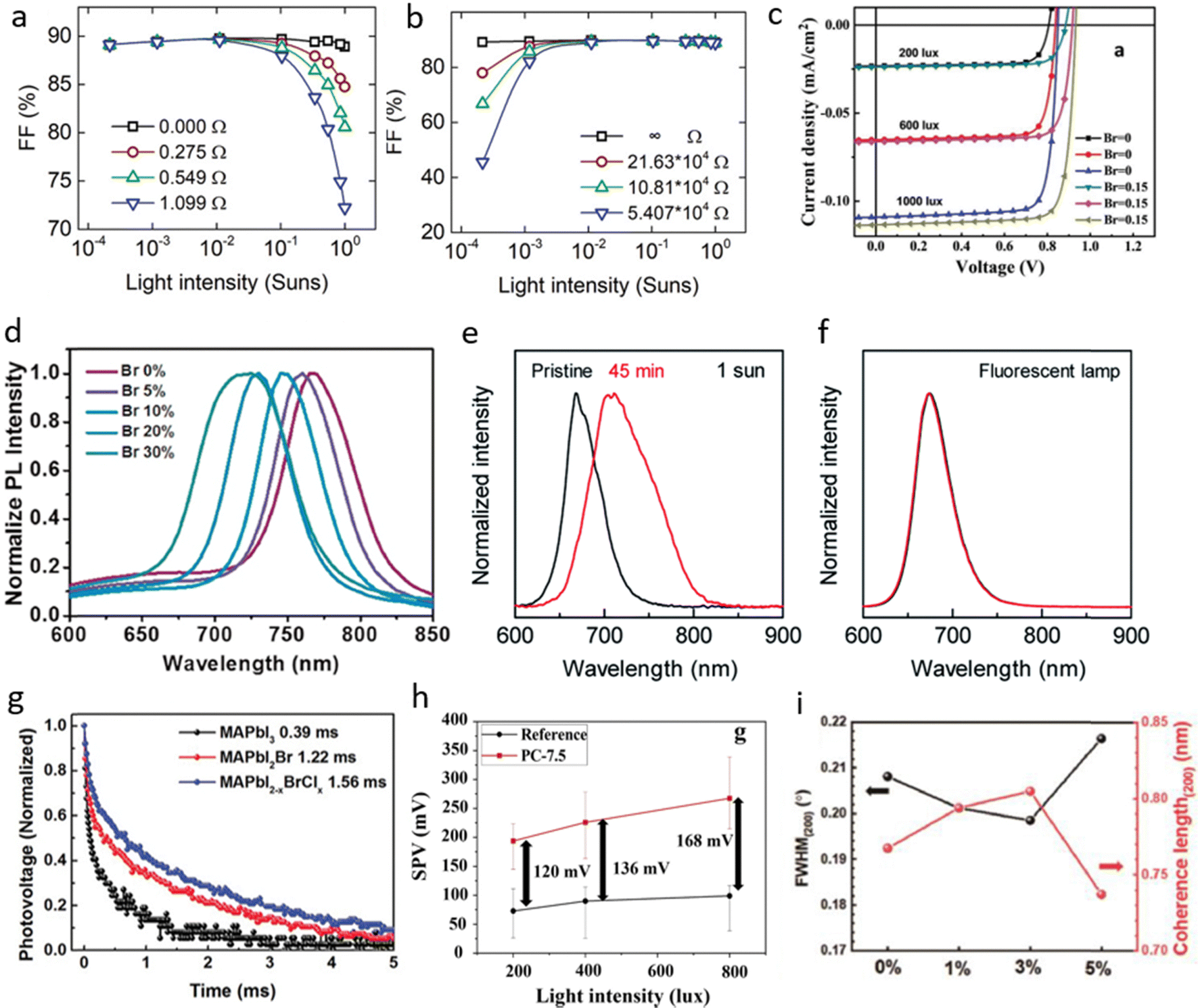 | ||
| Fig. 1 Simulated results for FF of PSCs under different light intensities: (a) devices having only (a) series resistance, and (b) shunt resistance as performance-limiting factor. Reproduced with permission.32 Copyright 2021, John Wiley and Sons. (c) J–V curves of PSCs under different light intensity. Reproduced with permission.33 Copyright 2019, John Wiley and Sons. (d) PL spectra of the MAPbI3−xBrx films.34 Copyright 2020, Elsevier. (e) PL spectra of Cs0.05FA0.79MA0.16Pb(I0.50-Br0.50)3 (FA = formamidinium, MA = methylammonium) films under AM 1.5G illumination, and (f) under FL illumination. Reproduced with permission.35 Copyright 2019, RSC Publishing. (g) Transient photovoltage decay under open circuit condition. Reproduced with permission.36 Copyright 2019, John Wiley and Sons. (h) Mean CPD values obtained in the dark and under 200, 400, and 800 lux. (i) Full width at half maximum (FWHM) and coherence length of crystals for (200) phases. Reproduced with permission.37 Copyright 2020, Elsevier. | ||
2.3. Trap-assisted recombination
Experimentally, besides the parasitic resistance, other resistances originate from defects might induce energy dissipation that can reduce the PCE of the device. Therefore, independent analysis of Rs and Rsh will be irrelevant for further analysis. The trap-assisted recombination, that takes place mostly at the grain boundaries and interfaces, plays a big role in providing recombination sites which influences a lot to the reduced efficiency of PSCs.38 It usually referred as interface recombination center (non-radiative recombination center). Not only that, but the defects might be generated within the perovskite crystal during fabrication process, which commonly known as bulk recombination center (Shockley–Read–Hall (SRH) trap-assisted and radiative recombination center). These two recombination centers operate differently under low light illumination. At higher light intensity, the number of photogenerated carriers is sufficient to overcome the bulk and interface recombination, whereas the remaining photogenerated carriers can be collected at the respective electrodes. However, at lower light intensity, the number of photogenerated carriers are more limited. Most of those photogenerated carriers recombine, leaving very less photogenerated carrier that can be converted to energy; subsequently drops the PCE.Even though both recombination centers are well known to deteriorate the performance of PSCs, but interface recombination mechanisms are dominating at high light intensities.39 There is a high concentration of defects within a few nanometers of the interface, caused by dangling bonds and structural mismatches between the adjacent surfaces. Moreover, the higher concentration of photogenerated carriers gained at higher light intensity give rise to more carriers that can reach the surface. Thus, more carriers recombine non-radiatively at the surface. It also explains the reason many researchers are working on interface engineering for highly efficient and stable PSCs.40,41 Meanwhile, at lower light intensity, bulk recombination is more detrimental to IPSC performance than interface recombination, due to larger FF drop.32 Nevertheless, both recombination centers should be mitigated properly for fabricating IPSCs with a performance close to the Shockley–Queisser (S–Q) limit. One of them is by the composition engineering of perovskite absorber films which is important to not only obtaining appropriate bandgap, but also overcome the bulk recombination center.
2.4. Optimized light extraction through bandgap engineering
As mentioned in previous chapter, to extract the most energy from indoor lamps including FLs, phosphorous LED, red-green-blue LED, and other indoor lamps, PSCs with an optimal bandgap between 1.70–2.00 eV is necessary. A wider bandgap of perovskite films can be achieved by introducing a mixed-halide perovskite composition, specifically by employing higher portion of bromine into the perovskite films.34 Even though, the devices prepared with pure iodine-based perovskite and iodine–bromine-mixed perovskite showed similar performance under 1 sun illumination, they performed differently under low light intensity.33 Thus, it is important to understand the influence of bromine inclusion into perovskite active layer.To get the most efficient wide bandgap PSCs, the fraction of Br should be optimized. Nonetheless, rather than improving the efficiency, PSCs with excessive addition of bromine in the active layer would perform poorly due to the changes in the morphologies. For example, Wu et al. employed the bromine additives into MA0.85Cs0.15PbI3 perovskite film to adjust the bandgap from 1.59 to 1.66 eV.33 Not only adjusting the bandgap, the optimized bromine addition showed lower defect density level as can be seen from the lower photoluminescence (PL) decay and larger grain size, implying better morphology which was preferable for high performing IPSCs. Similarly, Lim et al. showed that the optimized condition with precise concentration of Br in pure MAPbI3 perovskite system (the change of PL peak, corresponding to bandgap, as a function of Br addition are shown in Fig. 1d) led to the formation of an uniform perovskite films with low trap density which originated from lowered interfacial pinholes and recombination sites.34 Consequently, it improved charge collection efficiency, as can be seen from the enhanced crystallinity and lower PL decay. In conclusion, not only improving the devices performances via morphology and defect regulation, which is beneficial for obtaining high current density, but Br addition also enhancing the Voc of the devices due to the widening of the bandgap. As a result, higher performance of IPSCs can be obtained.
2.5. Phase segregation of perovskite films
Although the mixed-halide perovskite with an optimized condition showed better PSCs performance under low light illumination, any phase segregation of any system with mixed composition should be considered. Singh et al. explored the effect of perovskite crystal structure with different combination of iodine and bromine in MA-based perovskite absorber to compare the electrical conductivity, trap density, recombination loss, and operational stability of the PSCs.42 In contradiction, they found that the stability of tetragonal phase of pseudo halide perovskite based PSCs with mixed iodine and bromine were inferior as compared to the pure crystalline cubic phase of the MAPbI3 and MAPbBr3 perovskites due to unstable tetragonal phase induced by phase segregation. In fact, in-line with previous discussion, excessive bromine fraction in the mixed-halide perovskite system influences the morphology and opto-electronic properties of the films. Fortunately, as shown in Fig. 1e, and f, phase segregation, which typically occurs in mixed-halide perovskite systems under 1 sun illumination, was not observed under low light illumination, specifically by adding more cations into the system, making a mixed-cation perovskite composition of Cs0.05FA0.79MA0.16Pb(I0.5Br0.5)3.43 As can be seen from the PL data, there was no phase segregation occurred even after 45 minutes of continuous fluorescent light irradiation, which was prominent under 1 sun light illumination. This result showed the cation engineering of perovskite film with mixed halide perovskites, similar to recent study,44 should be further explored to fully harness their potential for IPSC applications.2.6. Defect suppression with multiple anions
To further improve the performance of PSCs under low light illumination, perovskite with multiple anions were studied. This multiple anion composition is proven to be beneficial for: (1) suppressing non-radiative recombination loss, better than only Br-doping.45 It was found that halide segregation, which usually happens in Br–I perovskite system, can be retarded by the chloride addition. Moreover, it also reduced the trap-states, leading to enhanced transient photovoltage decay as shown in Fig. 1g. It was proven from the outstanding long-term stability where in retained over 95% of original efficiency under 2000 hours light soaking; (2) eliminating bulk defects: chlorine incorporation into the perovskite layer influences the movement of photogenerated carriers and ions because of the smaller bulk defects in perovskite, which enhanced the hole extraction on the top surface.36 Moreover, from the mean contact potential difference measurement using Kelvin probe force microscopy (KPFM) (Fig. 1h), it was found that the chlorine inclusion also contributed to better hole extracting property on the perovskite surface, owing to less defect in the bulk; and (3) regulating crystallization kinetics and forming an improved crystallinity, where the lattice structure caged by the partial Cl− substitution, resulting a larger grain size, less defects, and a more favorable uniform surface.46 A high quality of CsPbI2Br was fabricated by incorporating CsCl as a doping: resulting in improved crystallization kinetics with flat, dense, and large-sized grains of perovskite films, as shown from narrowest full at half maximum of (200) peak.47 Similarly, high crystallinity CsPbI2Br perovskite films was obtained by incorporating tetramethylammonium chloride (TMACl) as an additive: producing pinholes-free compact grains, smooth surface, reduced trap density, and better phase stability in Fig. 1i.37 Consequently, the improved properties resulted in suppressed recombination and longer carrier lifetime, which ultimately enhanced the devices performance.In summary, wide bandgap perovskite film fabricated with bromine addition is necessary for IPSC applications. However, the bromine inclusion to the perovskite film should be optimized that wider bandgap close to 1.7–2.0 eV is achieved without inducing phase segregation problem which proven to be detrimental for the IPSCs performance. The cation engineering can compensate the unfavorable tetragonal crystal structure from stable cubic crystal structure induced by halide modification.
3. Recent research advances in IPSCs
In recent years, IPVs have gained significant attention for their applications in low-light environments, encompassing various material systems such as silicon, dye-sensitized, III–V, organic, and PSCs, as summarized in Table 1. Silicon-based IPVs offer high stability and mature manufacturing but are limited by poor spectral alignment indoors (PCE: 36% under 3000 lux LED).48 III–V cells achieve high PCEs (GaInP: 40.9% under 1000 lux LED) but are costly and less scalable. Organic photovoltaics (OPVs) feature tunable bandgaps and flexibility (PCE: 36.5%) but face challenges with low carrier mobility and structural disorder.49 Dye-sensitized solar cells (DSSCs) excel in spectral adaptability (PCE: 34.5%) but are hindered by electrolyte volatility and encapsulation issues.50 By contrast, PSCs stand out for their tunable bandgaps, defect tolerance, high quantum efficiency, and simple fabrication, achieving a record PCE of 42.43% under indoor conditions.51 IPSCs demonstrate unparalleled potential as the next-generation technology for indoor energy harvesting, combining superior performance with flexibility and cost-effectiveness to outpace traditional material systems.| Year | Com. | E g | Area (cm2) | J sc (mA cm−2) | V oc (V) | FF (%) | PCE (%) | PV type | Light source | Light intensity (lux μW−1 cm−2) | Ref. |
|---|---|---|---|---|---|---|---|---|---|---|---|
| a GaInP: gallium indium phosphate. b GaAs: gallium arsenide. c GIGS: copper indium gallium selenide. | |||||||||||
| 2024 | FA0.85MA0.15PbI3 | 1.54 | 0.09 | 0.144 | 0.984 | 83.24 | 42.12 | PSC | LED 3000 K | 1000/280 | 52 |
| 0.09 | 0.072 | 0.931 | 138 | 39.31 | LED | 500/138 | |||||
| 0.09 | 0.032 | 0.899 | 26 | 38.31 | LED | 200/56 | |||||
| Cs0.05FA0.85MA0.10Pb(I0.97Br0.03)3 | 1.61 | 0.0623 | 0.138 | 1.08 | 83.43 | 41.04 | LED 3376 K | 984/300 | 53 | ||
| Cs0.05FA0.85MA0.1Pb(I0.97Br0.03)3 | 1.52 | 0.0623 | 0.137 | 1 | 77.2 | 35.14 | LED 3300 K | 984/300 | 54 | ||
| Cs0.18FA0.82Pb(I0.8Br0.2)3 | 1.65 | 0.1 | 0.293 | 1.04 | 77.3 | 42.05 | LED 3000 K | 1000/596 | 55 | ||
| FA0.92MA0.08PbI3 | 1.55 | 0.09 | 0.13 | 1.148 | 85.17 | 45.51 | LED 3000 K | 1000/279 | 56 | ||
| Cs0.05FA0.70MA0.25PbI2.25Br0.75 | 1.71 | 0.0915 | 1.069 | 82.3 | 44.72 | U30 light | 1000/338.2 | 57 | |||
| CsPbI3 | 1.79 | 0.045 | 0.160 | 0.97 | 75 | 41.1 | FL | 1000/300 | 58 | ||
| 0.130 | 0.992 | 77.4 | 39.2 | LED 3000 K | 1000/ | ||||||
| Cs0.15FA0.85PbI3 | 1.48 | 0.157 | 0.93 | 83.15 | 39.04 | LED 6500 K | 1000/ | 59 | |||
| 2023 | CsPbI2.85Br0.15 | 1.74 | 0.09 | 0.173 | 1.012 | 77.66 | 39.78 | LED | 1200/341 | 60 | |
| FAPbI3 | 1.54 | 0.09 | 0.145 | 0.994 | 82.53 | 42.43 | 1002/281 | 61 | |||
| CsPbI3 | 1.7 | 0.09 | 0.155 | 1.07 | 83 | 41.21 | LED 2956 K | 1062/334.11 | 62 | ||
| Cs0.18FA0.82Pb(I0.8Br0.2)3 | 1.64 | 0.1 | 0.278 | 1.07 | 79.2 | 39.9 | LED 3000 K | 1000/284.4 | 63 | ||
| CsPbI2Br | 1.93 | 0.04 | 0.137 | 1.041 | 80.62 | 30.43 | LED | 1000/379.54 | 64 | ||
| CsPbI3 | 1.7 | 0.09 | 0.143 | 1.02 | 0.82 | 38.93 | LED | 1000/307 | 65 | ||
| 2022 | FA0.83MA0.17PbI2.53Br0.47 | 0.09 | 0.245 | 0.83 | 0.53 | 32.61 | 1000/ | 66 | |||
| FAPbI3 | 1.52 | 0.0725 | 0.150 | 0.920 | 77.1 | 31.85 | LED 2956 K | 1062/334 | 67 | ||
| CsI0.05((FAPbI3)0.85(MAPbBr3)0.15)0.95 | 1.58 | 0.1 | 0.107 | 1 | 82 | 36.9 | LED | 800/ | 68 | ||
| MAPbI3 | 1.66 | 1 | 0.051 | 0.85 | 74 | 33.8 | LED | 2851/100 | 11 | ||
| Cs0.17FA0.83 Pb(I0.7Br0.3)3 | 1.72 | 0.1 | 0.1594 | 0.926 | 82.5 | 30.9 | LED 3270 K | 1000/393.6 | 69 | ||
| Cs0.17FA0.83PbI1.8Br1.2 | 1.77 | 12.96 | 0.274 | 6.42 | 73 | 36.36 | TL84 | 1000/ | 70 | ||
| 0.09 | 0.122 | 1.03 | 79.79 | 32.94 | LED 3000 K | 1000/301.9 | |||||
| FA0.92MA0.08PbI2.92Br0.08 | 1.53 | 24 | 0.0171 | 7.678 | 72.39 | 30.73 | LED 6600 K | 1000/310 | 71 | ||
| 0.0142 | 7.605 | 73.22 | 26.48 | Yellow LED 3000 K | 1000/298 | ||||||
| 2021 | (FAPbI3)0.97(MAPbBr3)0.03 | 1.59 | 0.08 | 0.152 | 1.001 | 79.52 | 40.1 | LED 2700 K | 824/301.6 | 72 | |
| MAPbI3 | 1.5 | 0.02 | 0.165 | 0.93 | 82.1 | 39.2 | LED 2700 K | 1000/ | 27 | ||
| Cs0.05(FA0.6MA0.4)0.95Pb(I0.6Br0.4)3 | 1.75 | 0.02 | 0.135 | 0.95 | 69.6 | 33.42 | LED | 1000/ | 25 | ||
| CsPbBrI2 | 1.89 | 0.09 | 0.15 | 0.94 | 80 | 33.5 | FL 2956 K | 1062/334.41 | 73 | ||
| CsPbBrI2 | 1.89 | 0.17 | 0.75 | 62 | 28.48 | FL | 1000/ | 74 | |||
| MA0.91FA0.09PbI0.94Br0.06 | 1.58 | 0.2 | 0.188 | 0.96 | 78.7 | 38.2 | LED 5000 K | 1000/370 | 75 | ||
| CsPbI2Br | 1.91 | 0.09 | 0.1998 | 1.13 | 86.34 | 34.2 | LED | 400/120 | 76 | ||
| 0.9553 | 1.23 | 82.07 | 32.6 | LED | 1000/300 | ||||||
| 2020 | Hydrogenated amorphous silicon | 1.81 | 0.25 | Si | Warm-white LED 3000 K | 1000/300 | 48 | ||||
| 2020 | Hydrogenated amorphous silicon | 1.81 | 0.25 | 0.6929 | 0.725 | 65.9 | 36 | Si | 3000/920 | 77 | |
| 2015 | Crystalline Si | 1.68 | 0.0812 | 0.25 | 48.1 | 6.11 | Si | FL | 500/ | 78 | |
| 2015 | Crystalline Si | 1.68 | 0.0775 | 0.22 | 45.4 | 4.73 | Si | LED | 500/ | ||
| 2015 | Crystalline Si | 1 | 0.02 | 0.37 | 64 | 9.19 | Si | 209/62.9 | 79 | ||
| 2015 | Amorphous silicon | 1 | 0.02 | 0.61 | 66 | 10.51 | Si | 209/62.9 | |||
| 2023 | GaInPa | 1.89 | 4 | 0.085 | 1.17 | — | 26.8 | III–V | LED 3000 K | 1000/— | 80 |
| 2023 | GaInP | 1.89 | 1 | 0.1122 | 1.354 | 83.4 | 40.9 | III–V | LED | 1000/ | 81 |
| 2023 | GaInP | 1.89 | 1 | 0.0112 | 1.276 | 81.3 | 37.5 | III–V | LED | 100/ | |
| 2015 | Al0.2Ga0.8As | 1.67 | 0.01 | 0.045 | 0.85 | 79 | 21.1 | III–V | White LED | 580/100 | 82 |
| 2015 | Al0.2Ga0.8As | 1.67 | 0.01 | 0.85 | 79 | III–V | White LED | 1000/ | |||
| 2015 | Al0.2Ga0.8As | 1.67 | 0.01 | 0.78 | 77 | III–V | White LED | 20/ | |||
| 2021 | GaAsb | 1.43 | 48 | 0.0408 | 2.31 | 44.1 | 14.1 | III–V | Warm LED 3000 K | 1000/293 | 83 |
| 2020 | GaAs | 1.43 | 4 | 0.1271 | 0.816 | 64.5 | 22.85 | III–V | LED 3000 K | 1000/292.67 | 84 |
| 2020 | GaAs | 1.43 | 4 | 0.1285 | 0.817 | 64.3 | 21.72 | III–V | LED 4000 K | 1000/310.79 | |
| 2020 | GaAs | 1.43 | 4 | 0.1471 | 0.824 | 63 | 20.62 | III–V | LED 6000 K | 1000/370.19 | |
| 2023 | CIGSc | 1.17 | 0.5 | 0.1143 | 0.516 | 65.5 | 12.5 | III–V | LED | 1000/ | 81 |
| 2023 | CIGS | 1.17 | 0.5 | 0.0115 | 0.36 | 33.8 | 4.5 | III–V | LED | 100/ | |
| 2024 | PYFO-V | 1.98 | 0.1319 | 0.829 | 75.4 | 25.9 | OPV | LED 2600 K | 1000/318 | 85 | |
| 2024 | PYFO-V | 1.98 | 0.2638 | 0.855 | 76.1 | 27.1 | OPV | LED 2600 K | 2000/637 | ||
| 2023 | PM6:L8-BO | 1.6 | 0.048 | 0.1385 | 0.81 | 80.97 | 29.52 | OPV | White LED 3000 K | 1000/ | 86 |
| 2023 | PB2:FCC-Cl | 0.04 | 2.53 | 1.02 | 80.5 | 33 | OPV | LED 2700 K | 20![[thin space (1/6-em)]](https://www.rsc.org/images/entities/char_2009.gif) 000/ 000/ |
87 | |
| 2023 | PM6:Y6:2PACz | 1.74, 133 | 0.045 | 0.1466 | 0.72 | 77 | 36.4 | OPV | LED | 1000/230 | 49 |
| 2023 | PM6:Y6:2PACz | 1.74, 133 | 0.045 | 0.1626 | 0.722 | 77.5 | 33.7 | OPV | FL | 1000/270 | |
| 2024 | XY1b TiO2 hollow sphere | 0.2195 | 0.64 | 53.8 | 25.25 | DSSC | LED | 1000/300.7 | 88 | ||
| 2024 | N719 + Ti, CNT | 0.0019 | 0.2618 | 0.583 | 69.75 | 25.53 | DSSC | FL U30 | 1500/ | 89 | |
| 2024 | N719 + Ti, CNT | 0.0019 | 0.1724 | 0.564 | 70.58 | 24.29 | DSSC | FL U30 | 1000/ | ||
| 2023 | D35:XY1 DMP-5 electrolyte | 1 | 0.1349 | 0.91 | 82.6 | 35.6 | DSSC | Warm white CFL 2700 K | 1000/283.4 | 90 | |
| 2023 | D35:XY1 DMP-5 electrolyte | 1 | 0.1149 | 0.893 | 80.1 | 29.8 | DSSC | Warm white LED 2700 K | 1000/303.2 | ||
| 2021 | MS5, XY1b | 1.72 | 2.8 | 0.387 | 0.98 | 81.5 | 34.5 | DSSC | Warm white FL | 1000/318.2 | 50 |
| 2020 | XY1, L1 | — | 0.16 | 0.147 | 0.75 | 77 | 34.0 | DSSCa | FL | 1000/103 | 91 |
Achieving high PCE and operational stability in PSCs under low illumination hinges on meticulous control over nucleation and crystal growth during film formation. A well-regulated crystallization process yields uniform films with minimal defects, enhanced carrier mobility, and superior light absorption—key factors for optimal indoor performance.52,92 Similarly, defect passivation is particularly crucial for IPSCs, as intrinsic and extrinsic defects in perovskite films can serve as recombination centers, limiting charge carrier lifetimes and reducing efficiency.93 Over the years, various methodologies have been developed to mitigate these defects, including doping strategies, the use of small molecules and organic additives, and interfacial engineering.92,94,95 This section highlights recent noteworthy achievements in IPSCs, emphasizing methodologies for crystallization control and defect passivation, and their practical applications in improving efficiency and stability.
3.1. Improving perovskite film quality via nucleation and growth control
The primary reason for large energy loss in halide perovskites is ascribed to the slow nucleation and fast crystallization of the films. Especially, tin-based perovskites, with their narrow bandgap and high carrier mobility, are promising candidates for the preparation of efficient lead-free PSCs. However, the poor crystallization of tin-based perovskite films with unfavorable defects and rough morphology is still the biggest challenge to achieve high PCE.Wang et al. presents a novel strategy for achieving rapid nucleation and slow crystal growth of CsPbI3 perovskite films using solvent molecular sieves in the antisolvent.96 A mixed chlorobenzene and ethyl alcohol antisolvent induces rapid nucleation through supersaturation, while small molecules like phthalimide regulate solvent evaporation and crystal growth. Phthalimide acts as a molecular sieve, passivating surface defects and enhancing performance. This approach achieves high-crystallinity films with large grains and minimal defects. The resulting device demonstrates a PCE of 20.14% under AM1.5G and 40.07% under 1062 lux LED, offering a pathway to stable, high-quality inorganic perovskite films for indoor and outdoor applications.
Dong et al. introduces lead oxalate (PbC2O4) as a non-halide lead component in the perovskite precursor solution, which facilitates anion replacement during thin film annealing.29 The interaction between PbC2O4 and MAI moderates nucleation and crystallization, producing films with larger grains and fewer defects. Fig. 2a briefly illustrates the crystallization process of perovskite layers during annealing. The J–V curves in Fig. 2b indicate that Voc has the most significant impact on device performance, which is attributed to interface adjustments between the active and charge-transporting layers. These adjustments reduce interfacial electron–hole recombination, while minimal trap levels at the interface enhance carrier transport, thereby boosting device efficiency. Controlled crystallization prevents C2O42− penetration into deeper layers due to ionic radius differences, optimizing surface properties. Adjustments at the active layer interfaces reduce electron–hole recombination and enhance carrier transport, boosting efficiency. The optimized device achieved a Voc of 1.12 V, a PCE of 20.20% under standard illumination, and 34.86% under 1000 lux. Additionally, PbC2O4 improves performance consistency, as shown by reproducible PCE results across multiple devices (Fig. 2c).
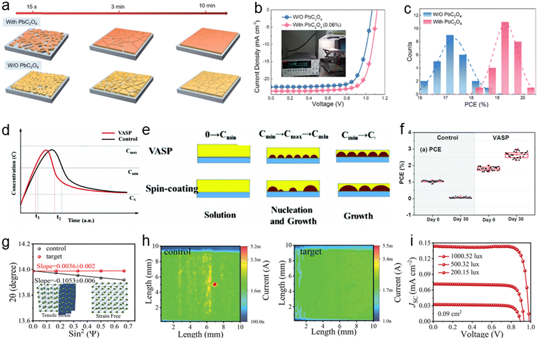 | ||
| Fig. 2 (a) Schematic illustration of the annealing process for perovskite film deposition from precursors with or without PbC2O4. And (b) J–V curves of control and doped devices under 100 mW cm−2 illumination. And (c) distribution chart of PCE for control and optimal devices. Reproduced with permission.29 Copyright 2024, American Chemical Society. (d) Comparison of nucleation and growth predictions using the LaMer model for the VASP method and the spin-coating method. And (e) schematic illustrations showing the nucleation/growth competition according to each method. (f) PCEs of the control device and the VASP device. Reproduced with permission.97 Copyright 2024, American Chemical Society. (g) and (h) 2θ–sin2ψ plots and transient photogenerated current mappings for the control and target films. (i) J–V curves of the target IPSC under light densities of 1000, 500, and 200 lux in a 0.09 cm2 area. Reproduced with permission.98 Copyright 2024, John Wiley and Sons. | ||
CsSnI3-based PSCs often suffer from Sn2+/Sn4+ oxidation and unbalanced nucleation and growth, hindering performance. To address this, Li et al. developed a vacuum flash-assisted solution processing (VASP) method for fabricating high-quality CsSnI3 films.97 Using the LaMer model, they demonstrated that rapid solvent evaporation in a low-pressure chamber achieves balanced nucleation and growth rates, see Fig. 2d. As illustrated in Fig. 2e, this process ensures high nucleation density, reduced pinholes, and enhanced crystal quality. Compared to spin-coating, VASP films exhibit better surface coverage, preferred facet orientation, reduced defects, and enhanced charge carrier mobility. These improvements lead to better charge transport, lower trap-assisted recombination, improved moisture stability, and significantly higher PSC efficiency. Fig. 2f shows that VASP cells achieved further PCE improvement, increasing from 2.0% to 3.8% over 180 days as Jsc and FF rose under nitrogen storage, due to gradual optimization of the crystal structure. In contrast, control cells completely lost their photovoltaic characteristics.
Li et al. introduced β-alaninamide hydrochloride (AHC) into the perovskite precursor solution to create 2D perovskite nucleation seeds, improving film uniformity, crystallinity, and reducing lattice stress.52 This in situ pre-nucleation approach facilitates the growth of high-quality 3D perovskite films with larger grains, enhancing charge carrier lifetime by tenfold. The resulting PSCs achieved PCEs of 42.12% for small areas (0.09 cm2) and over 40% for larger areas (1.00 cm2 and 2.56 cm2). Unsealed devices also exhibited excellent stability, retaining 90% efficiency after 6570 hours in dry storage and 83% after 920 hours of continuous light exposure in nitrogen.
In flexible IPVs, Kim et al. introduced butyl acetate (BA) as a green antisolvent to enhance perovskite film quality.99 Due to its low toxicity and a larger solubility parameter difference with DMSO compared to CB, BA facilitates gradual nucleation and crystallization, resulting in perovskite films with larger grain sizes (>1 μm), reduced trap density, and improved charge carrier mobility. Devices using BA achieved a PCE of 19.78% with 97.4% stability after 1000 hours. Under indoor illumination, they reached a PCE of 23.33% and a maximum power density of 0.104 mW cm−2. These devices also maintained performance under bending, making them ideal for wearable devices, low-power electronics, and BIPV applications. Li et al.98 proposed an in situ heterogeneous nucleation strategy, incorporating β-alaninamide hydrochloride (AHC) into the perovskite precursor solution. This additive spontaneously reacts with PbI2, leading to the formation of 2D perovskite seed crystals that guide the crystallization of high-quality 3D perovskite films. The 2θ–sin2ψ plots in Fig. 2g based on the grazing incidence X-ray diffraction (GIXRD) indicates the internal stress of the target perovskite films are almost completely released. Transient photogenerated current mapping (Fig. 2h) further demonstrated that the target film exhibited more uniform charge transport characteristics and lower trap density. Under a 1000 lux LED light source, the target i-PSC achieved a record-high 42.12% PCE, surpassing all previously reported values in the field. Even under reduced illumination intensities of 500 lux and 200 lux, the target device maintained outstanding efficiencies of 39.31% and 38.31%, respectively (Fig. 2i).
Advancements in nucleation and growth control has significantly enhanced the quality of perovskite films, leading to increased grain sizes, reduced defects, and improved device performance. Techniques such as additive incorporation and solvent engineering have been instrumental in optimizing crystallization, boosting both efficiency and stability. However, challenges remain in achieving a precise balance between nucleation and growth, as well as ensuring film uniformity for large-scale applications. These factors are critical for the scalability of high-performance perovskite solar cells in practical use.
3.2. Minimizing performance losses using defect mitigation strategies
Wide-bandgap PSCs face challenges like bulk trap-induced non-radiative recombination and bromine-rich perovskite segregation, leading to losses in Voc and FF. These issues are critical in IPVs, where low light generates fewer electrons than trapped electrons. Bulk trap recombination significantly impacts Voc and FF under low light intensity, with FF being more influenced by Rsh than Rs. To mitigate these effects, various passivation strategies have been explored, which will be discussed in the following sections.Kim et al. studied chlorine doping in perovskite precursors for indoor light applications, highlighting its role in improving PSC performance under low-intensity light. Chlorine doping reduces bulk defects, enhances carrier mobility, and facilitates hole extraction at grain boundaries, leading to better charge separation and reduced non-radiative recombination.36 The optimized (Pb(I0.98Br0.02)2)0.925(PbCl2)0.075 PSC (PC-7.5) achieved a maximum power density of 35.25 μW cm−2 under 400 lux LED light and 231.78 μW cm−2 under halogen illumination. Notably, KPFM measurements were conducted to compare the electrical properties of undoped (PC-0) and doped (PC-7.5) samples. The chlorine-doped PC-7.5 sample exhibited fewer trap sites at grain boundaries, enabling effective quasi-Fermi level splitting and significant band bending downward under illumination (Fig. 3a). The reference sample exhibited time-dependent contact potential difference (CPD) changes under illumination, attributed to ionic defect movement,100 while PC-7.5 showed stable CPD, indicating effective defect passivation (Fig. 3b). Higher surface photovoltage values for PC-7.5 across all light intensities confirmed lower non-radiative recombination and greater photo-generated hole accumulation, underscoring the benefits of chlorine doping in enhancing PSC stability and performance under indoor light conditions.
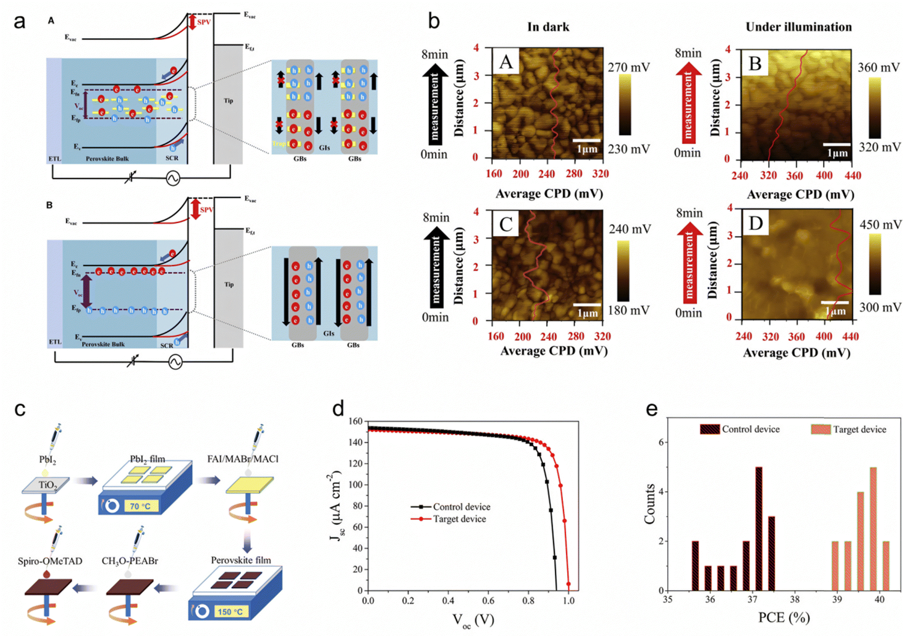 | ||
| Fig. 3 (a) Schematic band diagrams of the reference sample (A) and modified sample (B, PC-7.5) in the dark (black line) and under illumination (red line) and (b) CPD maps obtained by contact potential measurement in the dark for (A) the reference sample and (C) sample PC-7.5, and under 200 lux for (B) the reference sample and (D) sample PC-7.5, with an overlay of the CPD line profile. Reproduced with permission.36 Copyright 2024, Elsevier. (c) Preparation procedure for the perovskite film with an FTO/TiO2/perovskite/CH3O-PEABr/spiro-OMeTAD/Au structure. And (d) current density–voltage (J–V) curves for devices without (black) and with CH3O-PEABr (red) modification, and (e) PCE distribution histogram for the control and target PSCs measured under 824.5 lux (301.6 μW cm−2) LED illumination. Reproduced with permission.101 Copyright 2021, John Wiley and Sons. | ||
He et al. develops a passivation strategy incorporation of guanidinium and 2-(4-methoxyphenyl)ethylamine hydrobromide (CH3O-PEABr) to reduce traps both on the surface and in the bulk of micrometer-thick (FAPbI3)0.97(MAPbBr3)0.03 perovskite films, solving severe trap-induced nonradiative recombination, particularly under low-light conditions.101Fig. 3c illustrates the fabrication procedure of the (FAPbI3)0.97(MAPbBr3)0.03 perovskite film. Guanidinium forms 2D FAGAPbI4 perovskite, passivating grain boundaries, while CH3O-PEABr treatment reduces recombination at the perovskite/spiro-OMeTAD interface, resulting in smooth morphology and low trap activity. Significant PCE enhancement is mainly attributed to the Voc increase from 0.940 to 1.001 V and FF improvement from 77.99% to 79.52%, as shown in Fig. 3d. Fig. 3e displays the PCE distribution histogram for un-passivated control and passivated target PSCs based on 15 individual cells, with the narrower distribution of the target device indicating improved reproducibility due to trap passivation. Reduced nonradiative recombination enables a high Voc of 1.00 V, significantly enhancing the performance of micrometer-thick perovskite films and achieving a record PCE of 40.1% under 824 lux LED illumination.
In the meanwhile, Zhang et al. investigated the impact of Br vacancy (VBr) defects on wide-bandgap perovskites, revealing their significant contribution to Voc deficits.70 By fabricating I/Br hybrid MA-free perovskites with tunable bandgaps, they suppressed VBr defects using I-rich alkali metal compounds, particularly KI. This approach enhanced the Voc to 1.05 V under 1000 lux LED illumination, enabling a certified record PCE of 36.36% for an IPV module. This study highlighted that increasing Br content raised the minimum current from 30 to 45 pA and increased leakage current at grain surfaces, due to high defect density and rapid crystallization dynamics. Additionally, Br's high vapor pressure caused it to escape during annealing, leading to charged VBr accumulation and increased conductivity. These findings provide insights into mitigating Voc losses in wide-bandgap perovskites through defect control.
The current research on doping strategies has led to significant progress in mitigating defects in PSCs, especially under low-light indoor conditions. Targeted doping with elements such as chlorine and guanidinium has shown improvements in photovoltaic performance by reducing bulk trap-induced recombination. However, these advancements mainly focus on incremental improvements rather than comprehensive breakthroughs in device efficiency or long-term stability. A crucial gap persists in understanding the long-term effects of these doping strategies when PSCs are exposed to real-world conditions, including variable indoor light intensities and temperature fluctuations.
In this regard, representative study on passivating surface defects, particularly those related to iodine vacancies (VI), was conducted by Guo et al.102 In their study, they explored the use of 2,5-thiophenedicarboxylic acid (TDCA) to passivate VI through the strong coordination interaction between the thiophene unit of TDCA and the undercoordinated Pb2+ in the perovskite. TDCA interacts strongly with undercoordinated Pb2+via its thiophene unit, as confirmed by density functional theory (DFT) calculations. Introducing TDCA increased the VI formation energy from 1.411 to 1.885 eV, indicating effective defect passivation. This also elevated the perovskite surface valence band, enhancing interfacial energy alignment. TDCA passivation improved the performance of CsPbI2.25Br0.75 PSCs, increasing Voc from 1.36 to 1.43 V and efficiency from 15.55% to 16.72%, reaching 92% of the S–Q limit. Similar gains were observed in CsPbI1.5Br1.5 and CsPbIBr2 PSCs, with Voc improvements to 1.51 V (90% of the limit) and 1.54 V (87%), respectively, under 200 lux LED illumination, demonstrating its effectiveness for solving the problem of severe Voc deficits in CsPbX3 perovskites.
Zhang et al. designed a trifluoroacetamidine (TFA) passivator, to suppress CsPbI3−xBrx film interfacial defects. The amidine group of TFA strongly chelates to the perovskite surface, suppressing iodide vacancies and strengthening bonds through additional H⋯I hydrogen interactions. The three fluorine atoms enable strong intermolecular hydrogen bonds, constructing a robust shield against moisture.60 Moreover, This surface treatment also improves energy-level alignment at the perovskite/spiro-OMeTAD interface, reduces surface roughness, and lowers interfacial charge transfer resistance. Molecular interaction calculations showed highly favorable bond formation, with the TFA–Pb bond's formation energy at −1.96 eV, significantly more negative than that of the TFE–Pb bond (−0.52 eV) in Fig. 4a. Hydrogen bonds, such as H⋯I (−1.33 eV) and H⋯F (−0.57 eV), further enhanced surface adsorption (Fig. 4b). As a result, the champion TFA-treated device demonstrated excellent optoelectronic properties, achieving a PCE of 39.78% with a Voc of 1.012 V, a Jsc of 172.58 μA cm−2, and an FF of 77.66% under indoor light illumination (1200 lux, 341 μW cm−2) (Fig. 4c), setting a new benchmark for efficiency in all-inorganic photovoltaic devices under indoor light. Their treatment also improved stability, maintaining the black phase for 168 hours and 93% of initial PCE after 960 hours, demonstrating its effectiveness in enhancing both performance and durability.
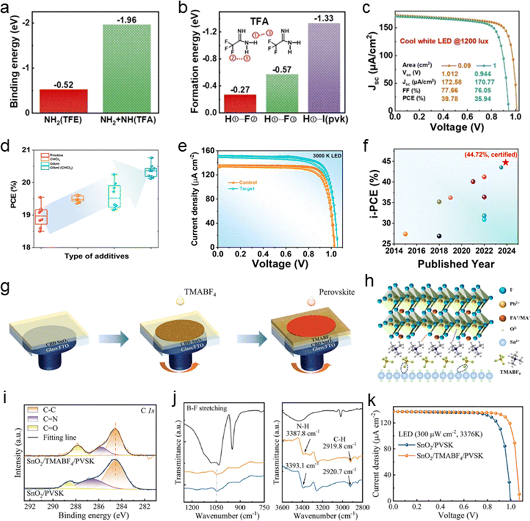 | ||
| Fig. 4 (a) The comparative calculated binding energies of NH2–Pb2+ and NH+NH2–Pb2+ for TFE and TFA, respectively. And (b) the calculated formation energies of H①–F②, H①–F③, and H①–I (perovskite) interactions for TFA. And (c) J–V curves of TFA-CsPbI3−xBrx-based solar cells with effective cell areas of 0.09 and 1.0 cm2 under 1200 lux (341 μW cm−2) illumination. Reproduced with permission.60 Copyright 2022, John Wiley and Sons. (d) Statistical deviations of PCE for WBG PSCs incorporating various additives. And (e) J–V curves representing IPVs performance of control and target WBG PSCs under LED light at 1000 lux. And (f) summary of i-PCEs from representative studies (2014–2023). Reproduced with permission.57 Copyright 2024, Royal Society of Chemistry. (g) Deposition procedure for the solar cells. (h) Schematic diagram of the bridge function at the buried interface. (i) C 1s XPS spectra of the control and target films. (j) FTIR spectra of TMABF4 (black), perovskite based on SnO2 (yellow) and SnO2/TMABF4 (blue). (K) Champion device J–V curves of the control and target devices under 300 μW cm−2 LED light. Reproduced with permission.103 Copyright 2024, John Wiley and Sons. | ||
Ma et al. developed a dual-additive strategy using oleylammonium iodide (OAmI) dissolved in trichloromethane (CHCl3) to enhance perovskite crystal growth and film quality.57 The dual additives significantly reduce bulk-trap defects and mitigate phase segregation, resulting in high-quality perovskite films. The composite perovskite adducts formed exhibit high binding energy, improving substrate interaction and facilitating crystal growth. Comparative analysis of control and modified precursors (with CHCl3, OAmI, and OAmI pre-dissolved in CHCl3) demonstrated that OAmI passivates lead iodide defects at grain surface and promotes 2D perovskite formation at grain boundaries, while CHCl3 enhances crystallinity. The dual additive strategy using OAmI (CHCl3) proved most effective, delivering superior passivation and crystallinity, optimizing perovskite film quality and performance (Fig. 4d).
Compared to the control, the target WBG PSCs achieved a significantly enhanced i-PCE of 42.86% (certified 43.43%) under 1000 lux LED illumination, with a Voc of 1.06 V (1.052 V), Jsc of 151.93 μA cm−2 (144.50 μA cm−2), and FF of 81% (80.5%), as shown in Fig. 4e. The dual-additive treatment minimized bulk defects, stabilized mixed-halide perovskite phases, and reduced non-radiative recombination losses, resulting in higher Rsh and improved performance. This approach achieved a certified record indoor PCE of 44.72%, with a Voc of 1.069 V and an FF of 82.3% under U30 light (1000 lux, 338.2 mW cm−2), as presented in Fig. 4f. Jiang et al. utilized a dithieno[2,3-d:2′,3′-d′]thieno[3,2-b:3′,2′-b′]dipyrrole (DTPT)-based acceptor–donor–acceptor (A–D–A) derivative blended with PCBM as the electron transport layer (ETL) which can effectively passivates the perovskite interfacial defects for IPVs.63 DTPTCY coordinated with Pb2+ ions, preventing the reduction of Pb2+ to Pb0. The PCBM formed a fibril-like structure, significantly enhancing electron mobility, suppressing bimolecular recombination, and facilitating shorter extraction times in the device. The hybrid ETL minimized defects, reduced trap density, and addressed interface hydrophobicity, resulting in improved PCE and stability. Optimized Cs0.18FA0.82Pb(I0.8Br0.2)3 p–i–n PSCs achieved PCEs of 37.2% under TL84 and 39.9% under 3000 K LED (1000 lux) illumination. The DTPTCY-based device demonstrated stability, retaining 87% of its initial PCE after 30 days in 40% relative humidity without encapsulation, compared to 67% for devices without the hybrid ETL. This work highlights the importance of mitigating trap-induced nonradiative recombination and interface defects to enhance IPV performance, particularly under low light illumination.
IPSCs face efficiency limitations due to voltage loss at the buried interface, where photogenerated carriers are initially formed. Li et al.103 proposed a bipolar pseudohalide ammonium salt (BPHA) bridging strategy to address lattice misalignment and carrier transport inefficiencies at this critical interface. The deposition process, illustrated in Fig. 4g, integrates tetramethylammonium tetrafluoroborate (TMABF4)-modified SnO2 to optimize carrier transport at the buried interface. The bipolar bridging effect, as depicted in Fig. 4h, shows that the fluorine-rich BF4− anions passivate oxygen vacancies in SnO2, while TMA+ cations bind to halide vacancies in the perovskite. This dual functionality enhances crystallinity, reduces defect formation, and improves charge carrier separation. Fig. 4i presents C 1s X-ray photoelectron spectroscopy (XPS) spectra, highlighting shifts in binding energy indicative of defect passivation. Fourier-transform infrared (FTIR) spectroscopy (Fig. 4j) further validated the interaction between TMABF4 and SnO2/perovskite, demonstrating modified vibrational modes associated with defect passivation. These findings confirm that TMABF4 effectively stabilizes the interface, reducing non-radiative recombination. The performance of the optimized IPSC was significantly enhanced, achieving a remarkable i-PCE of 41.04% under 300 μW cm−2 LED illumination. The champion device exhibited a record-high Voc of 1.08 V, as shown in Fig. 4k. Compared to the control, which suffered from efficiency losses due to interfacial defects, TMABF4-treated devices demonstrated improved charge extraction and suppressed recombination losses.
To suppress intrinsic defects in the perovskite active layer, Han et al. utilized facile solvent-engineering strategy to effectively suppress both surface and bulk defects in indoor solar cells, achieving a high efficiency of 35.99% under 1000 lux LED illumination.104 By replacing dimethylformamide (DMF) with N-methyl-2-pyrrolidone (NMP) in the perovskite precursor, they significantly reduced surface and bulk defects, prolonged charge carrier lifetimes, and minimized non-radiative charge recombination. NMP's higher donor number (DN) and β values, compared to DMF, create hydrogen-bond-favorable intermediate structures with formamidinium iodide and lead halides. This interaction improves perovskite film quality by reducing interfacial halide deficiencies and enhancing uniformity in surface morphology and potentials. The resulting perovskite films showed restrained non-radiative recombination and improved overall device performance, demonstrating the effectiveness of NMP in passivating defects and boosting cell efficiency.
4. ML-driven designs for IPSCs
ML has rapidly become a powerful tool in perovskite research, enabling breakthroughs in material discovery, device optimization, and performance prediction by uncovering complex patterns and leveraging large datasets.105–107 In outdoor PSCs, ML has been applied to tasks such as defect analysis, stability optimization, interfacial engineering, and integrating experimental and data-driven models.108–115 While these advancements provide a strong foundation, the application of ML to IPSCs remain underexplored. Despite sharing similar material and structural foundations, IPSCs face unique challenges, including differences in light absorption, defect dynamics, and operational environments under indoor lighting conditions, which demand tailored ML strategies. By adapting insights from outdoor PSC research, ML has the potential to accelerate the optimization of IPSCs, enabling precise adjustments in properties such as band alignment, defect passivation, and interfacial engineering. This chapter explores the integration of ML in advancing IPSC development, focusing on material discovery, device optimization, and performance enhancement, while addressing the specific challenges posed by indoor lighting environments through the intersection of computational techniques and experimental studies.4.1. Transition from outdoor to indoor applications
To this day, a series of significant progresses have been achieved in data driven PSCs for outdoor application. However, substantial differences exist between indoor and outdoor environments, particularly in terms of illumination conditions and energy demands. Thus, adapting the successful ML-driven strategies developed for outdoor perovskite photovoltaic applications to indoor devices is of critical importance. This section explores key areas where ML can be applied to IPSCs, including bandgap tuning, the discovery of novel perovskite materials suited for indoor conditions, and elucidation of indoor-specific perovskite mechanisms.One widely studied approach leverages supervised learning algorithms to predict bandgaps based on known perovskite datasets or high-throughput computational data across various composition ratios. This approach utilizes fixed elements at the ABX3 sites, adjusting their ratios to achieve desired bandgap tuning. For example, Cai et al.119 employed a forward-inverse framework to optimize the bandgap in Sn–Pb alloyed perovskites (MASnxPb1−xI3). By developing an ML model that predicts the bandgap based on Sn–Pb compositions, they revealed an asymmetric bending relationship between Sn content and bandgap, which is difficult to achieve by the traditional fitting method (see Fig. 5a). They designed a bidirectional optimization process to determine the suitable Sn ratio to achieve an optimal bandgap of around 1.35 eV, aimed at maximizing PCE. Based on their prediction results, Fig. 5b shows the efficiency changes with the energy difference of HTL HOMO and the perovskite absorber (ΔH), the energy difference of ETL LUMO and the perovskite absorber (ΔL), and bandgap (Eg) in a 3D scattering way. Their study showed that a Sn ratio of 0.6 resulted in the lowest bandgap and optimized the PCE. In another study, Yang et al.120 adopted a multi-fidelity ML to efficiently screen and design perovskite alloy materials. They trained a multi-fidelity RF model on this data, using fidelity labels (e.g., GGA-PBE, HSE06, experimental data) to achieve accurate bandgap cross-fidelity predictions. Model predicted bandgap for over 150000 hypothetical compounds. Fig. 5c present ternary phase diagrams showing the bandgap variation with the B-site metal elements Ge–Sn–Pb established in their work. Based on this, the researchers identified thousands of potential high-performance perovskites. In the study by Rauf et al.,121 the authors proposed a multi-scale ML framework to analyze the effects of Br doping on the bandgap of tin-based perovskites (such as CsSnI3, MASnI3, and FASnI3). In their work, the electronic density and bandgap at different Br doping levels were calculated through DFT. During this process, they demonstrated that the DFT-1/2 method can effectively correct the underestimation of bandgap in Sn based perovskite system, as can be seen in Fig. 5d. Through ML modelling, they revealed the essential influence of bandgap on the PCE, validating the importance of bandgap tuning.
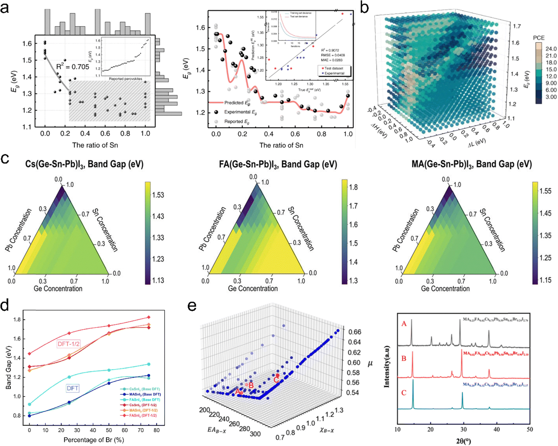 | ||
| Fig. 5 (a) The marginal histograms and traditional fitting result of Sn and bandgap, and the asymmetric bending relationship between Sn and bandgap. (b) The PCE variation along with the ΔH, the ΔL, and Eg. Reproduced with permission.119 Copyright 2022, Springer Nature. (c) The bandgap ternary diagrams of Cs(Pb–Sn–Ge)I3, FA(Pb–Sn–Ge)I3, and MA(Pb–Sn–Ge)I3. Reproduced with permission.120 Copyright 2024, AIP Publishing. (d) The bandgap changes of CsSnI3, FASnI3, and MASnI3 along with the Br percentage. Reproduced with permission.121 Copyright 2023, Elsevier. (e) Three validated compositions (red) and the training and test compositions (blue) in the feature space of the two most important features, and XRD patterns of the validated samples. Reproduced with permission.122 Copyright 2023, American Chemical Society. | ||
In most cases, the investigation about the influence of elemental ratios on bandgap begins with elemental doping combined with computational simulations. This approach presents three main challenges: (1) the doped elements are typically in small quantities, limiting the adjustable range of elemental ratios; (2) compositions were often adjusted along a single elemental site, resulting in data that fails to capture the global trend of bandgap variation; and (3) accurately modeling according to elemental ratios remains challenging, as finer control of elemental composition entails a higher atomic count in the model, leading to increased computational energy consumption. Obtaining data on material compositions and bandgaps from published sources or databases offers a viable alternative, but solvent and anti-solvent engineering pose challenges for collecting high-quality data. In Yang et al.'s study,122 a gradient boosting regression tree was used to predict the bandgaps of perovskite materials by integrating physical features. With this model, the bandgaps of 100000 virtual perovskite materials were screened, leading to the synthesis of materials with ideal bandgaps (MA0.23FA0.02Cs0.75Pb0.59Sn0.41Br0.24I2.76: 1.39 eV, MA0.02FA0.08Cs0.9Pb0.5Sn0.5Br0.9I2.1: 1.48 eV, MA0.2FA0.32Cs0.48Pb0.82Sn0.18Br1.83I1.17: 1.74 eV) suitable for photovoltaic applications, as illustrated in Fig. 5e. It is worth noting that their study aims to identify outdoor photovoltaic materials with minimal bandgaps based on the S–Q limit to achieve high PCE. For indoor perovskite materials, however, the focus should inversely shift toward identifying wide-bandgap candidates capable of absorbing indoor visible light. Exploring tunable bandgaps for indoor perovskites using ML remains a largely uncharted research area.
To find stable perovskites for oxide perovskite photovoltaic application, Talapatra et al.128 conducted large-scale ML screening, focusing on structures like A2B+B′3+O6, AAB′O6, and AA′B+B′3+O6. Two ML models were adopted: a classification model to categorize materials by bandgap width and a regression model to predict bandgaps. Finally, approximately 300 double oxide perovskites with substantial bandgaps were identified from 5 million candidates. Wei et al.129 proposed a novel framework combining domain knowledge and ML to predict physical properties of double halide perovskites (A2B+B′3+X6). By embedding domain knowledge through parameter initialization, the model improved R2 by 15.52% for bandgap and 5.65% for thermodynamic stability predictions across 540 perovskite materials. This approach significantly boosted prediction accuracy and accelerated the discovery of novel lead-free perovskites. Additionally, BaZrS3 has emerged as a promising photovoltaic material due to its strong light absorption and high carrier mobility. With a bandgap of 1.7 eV, making BaZrS3 an excellent candidate for indoor perovskites. Sharma et al.130 adopted ML to optimize the doping of BaZrS3. They generated datasets for bandgaps and formation energies of multiple doping combinations, covering 122500 possibilities. A RF model was trained to identify combinations with the suitable bandgap and high formation energy. ML predictions indicated Ca doping at the Ba site and Ti doping at the Zr site as the most effective strategies, with Ca doping providing enhanced stability and lowering the bandgap. Although their work focused on tuning BaZrS3 for outdoor PV use, but with larger atomic dopants at A and B sites and smaller dopants at X-site will favor wider bandgaps, which highlights the potential for indoor applications. In the research of López et al.,131 an integrated “bottom-up” approach for the material design of silver-bismuth halide MChX-type perovskites was proposed. They built a database covering 125 MChX compounds, calculating parameters such as lattice constants, formation energies, and bandgaps. Using CNN, they identified perovskites with outstanding optoelectronic properties, with bandgaps in the range of 1.2–2.1 eV and absorption coefficients reaching 6.6 × 105 cm−1 from a BixSb1−xSySe1−yIzBr1−z form dataset.
Compared to high-throughput computational methods, high-throughput experimentation (HTE) generates large-scale data directly under laboratory conditions, providing experimentally validated insights and capturing material behaviors that computational approaches often struggle to predict. This advantage enables more accurate guidance for optimizing material performance.132–134 Silver/bismuth-based organic–inorganic hybrid perovskites (AgBi-HOIPs), with absorption coefficients of 105–106 cm−1 and bandgaps of 1.8–2.0 eV, are promising for IPV applications. Studies on ABX compounds like Ag3BiI6 and AgBi2I7 reveal that their structures range from cubic (Bi-rich) to hexagonal (Ag-rich) forms, depending on the AgI to BiI3 ratio.135,136 As shown in Fig. 6a, Wu et al.137 developed a framework combining ML with HTE to accelerate the synthesis of novel 2D AgBi-HOIPs perovskite materials. They tested 80 organic amines (see Fig. 6b), achieving 14 successful and 66 unsuccessful syntheses of 2D perovskites. Using subgroup discovery, they identified favorable synthesis regions for 2D perovskites, and a support vector classification (SVC) model was developed to predict synthesis feasibility. They analyzed the feature contributions to synthesis viability and predicted 344 highly feasible candidates, of which 13 were experimentally validated. 8 candidates were successfully synthesized with bandgaps between 1.84 and 1.99 eV (Fig. 6c), which locate on the indoor bandgap range. In the other work shown in Fig. 6d, Sun et al.112 combined HTE with ML to successfully synthesize and characterize 75 perovskite-like thin films. This approach of accelerated experimentation and rapid data diagnostics enabled them to screen several lead-free perovskite candidates for photovoltaic applications. They utilized deep neural networks to process XRD data, categorizing the materials into 0D, 2D, and 3D structural dimensions, which significantly accelerated structural identification (Fig. 6e). They developed lead-free perovskite materials with bandgaps ranging from 1.2 to 2.4 eV, indicating their potential for indoor energy-harvesting devices.
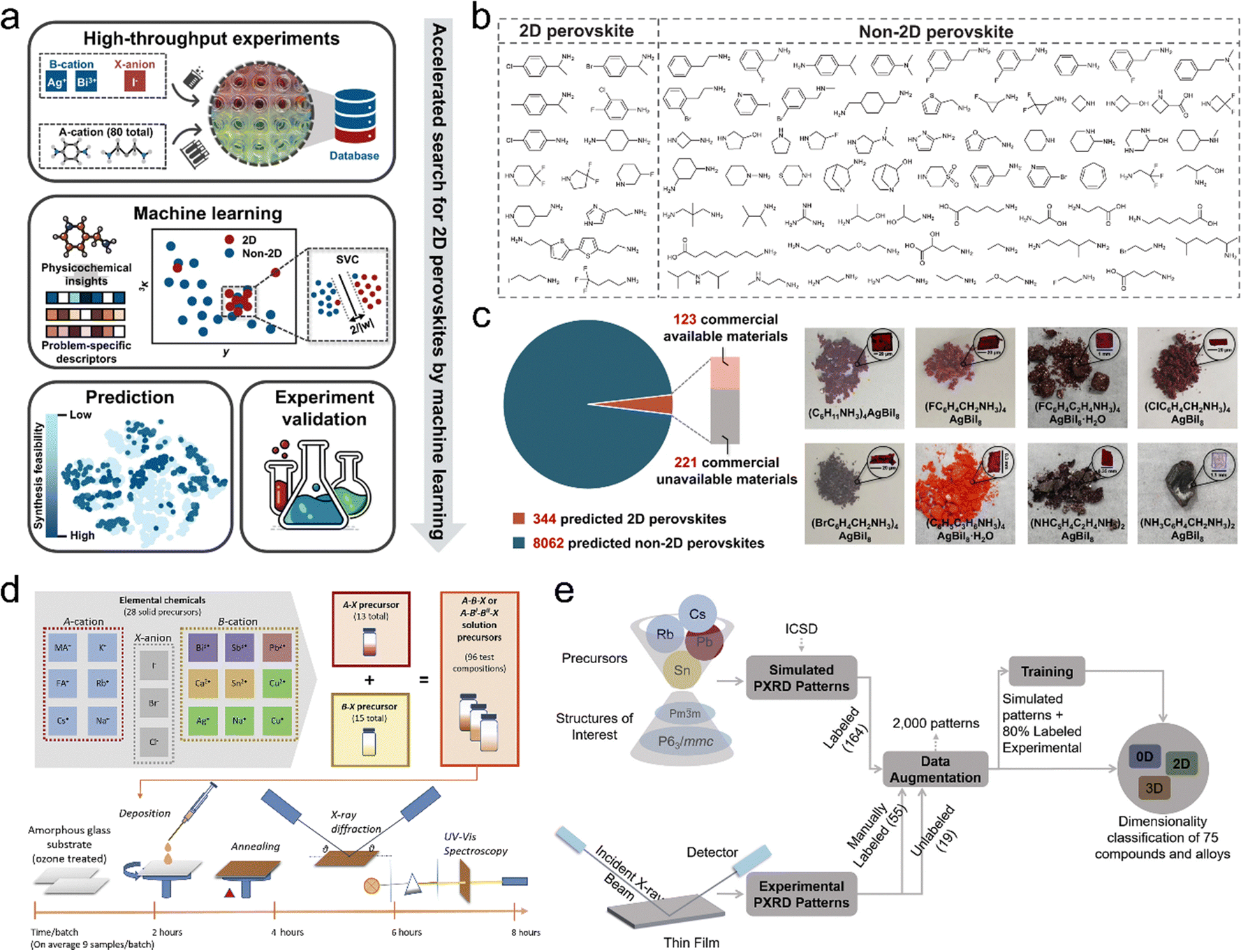 | ||
| Fig. 6 (a) Screening workflow for 2D silver/bismuth-based organic–inorganic hybrid perovskites. (b) Organic spacers of 14 successful and 66 unsuccessful syntheses of 2D perovskites. (c) The distribution of predicted perovskites, and the pictures of successfully synthesized candidates. Reproduced with permission.137 Copyright 2024, Springer Nature. (d) The workflow of the HTE: the selected elements were combined to synthesize precursors, and all successfully synthesized precursors experienced film deposition, X-ray diffraction, and UV-visible spectroscopy measurement to get the optical and structure information. (e) The framework that employing ML to assist structure characterization and guide the diagnosis results analysis. The input data are the 2000 augmented PXRD patterns data and the output is the crystal dimensionality. Reproduced with permission.112 Copyright 2019, Elsevier. | ||
4.2. Insights from mechanistic studies for IPSCs
Since IPSCs operate under low light intensities, high Rsh, energy-level mismatches at interfaces, energy loss, and non-radiative recombination are crucial factors affecting device performance. Therefore, how to enhance trap healing capabilities and minimizing interfacial trap-state defects are key challenges to enhance the output power of IPSCs. By integrating ML with large datasets, it is possible to deeply investigate defect-state characteristics, recombination mechanisms, and real-time tracking of device degradation.For investigating kinetics, Shi and Pullerits113 used tree-based and regression chain to fit PL data under various temperature conditions, revealing the carrier recombination kinetics in perovskite microcrystals. The activation energy and capture rate of trap states determine recombination dynamics at different temperatures, affecting optical performance. Their study leveraged ML algorithms for rapid fitting on modulated PL data, disentangling complex recombination processes and enabling high-reliability data interpretation to accurately predict carrier recombination characteristics. The Fig. 7(a) displays the detailed charger carrier kinetic of the MAPbBr3 under the room temperature, with PL emission of excitons (4 × 105 cm−3), free charge carriers (1 × 10⁶), trap depopulation (1.5 × 109 cm3 s−1), trapping process (4 × 109 cm3 s−1), and detrapping process (6 × 108 cm3 s−1). Liu et al.138 employed unsupervised learning to identify structural and electronic properties associated with trap formation. They uncovered a deep trap formation mechanism caused by bromine vacancy defects in Cs2AgBiBr6 double perovskite. As illustrated in Fig. 7b, the trajectories of Ag* and Bi* atoms around the negatively charged bromine vacancy (VBr−) show Ag* moving toward Bi* in the X–Y plane during trap-assisted charge recombination. They found that the negatively charged VBr− in Cs2AgBiBr6 forms deep traps through charge redistribution, in which the bromine vacancy induces electron transfer from Bi to Ag atoms, shifting trap states from shallow to deep levels. These deep traps accelerate non-radiative recombination, leading to charge loss and reduced device performance. By introducing indium (In) to replace Ag, the study showed that this doping strategy effectively suppresses deep trap formation, thereby maintaining the defect state at shallow levels and improving the optoelectronic stability.
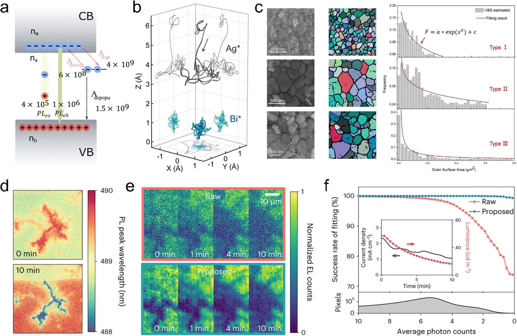 | ||
| Fig. 7 (a) The detailed charge carrier kinetics of MAPbI3 under the room temperature. Reproduced with permission.113 Copyright 2024, American Chemical Society. (b) Ag and Bi atom trajectories at vacancy sites of the VBr− system. Reproduced with permission.138 Copyright 2022, American Chemical Society. (c) SEM images of three typical perovskite grain surface area distributions, the extraction results by ML, and the statistical grain surface area distributions. Reproduced with permission.139 Copyright 2024, Elsevier. (d) The blue CsPbBr3 LED PL peak-wavelength map change after working 10 minutes. (e) The raw (upper) and CNN (lower) processed normalized EL intensity change maps with work time. (f) The success rate of the electroluminescence curve fitting against the average electroluminescence counts. The inset shows the current density and luminance vary with time. Reproduced with permission.140 Copyright 2023, Springer Nature. | ||
Simultaneously, image processing models demonstrate unique advantages in perovskite material characterization and mechanistic interpretation, efficiently identifying microstructures, defect distributions, and interfacial features to provide deeper data insights. These models automate complex analyses of microscopic images and spectroscopic data, reducing human error and enhancing the accuracy and speed of data interpretation.141,142 For IPSCs, interfacial traps are particularly influential, making interface characterization critical. The grain size and distribution have a strong correlation with the quality and device performance of perovskite thin films. The development of automatic grain characterization tools is of great significance for the study of perovskite.143–145 Zhang and Zhou139 proposed a ML-based method to extract grain surface areas, using a CNN combined with a U-Net structure to automatically segment the grain surface regions of perovskite films from SEM images. Fig. 7c displays three typical grain types and the extraction results by their model, grain distributions are accurately captured. This study also reveals correlations between grain microstructure and photovoltaic device performance: variations in grain surface area distributions lead to significant differences in PCE, particularly with larger grain areas positively affecting Voc and FF. So far, degradations caused by ion migration and phase separation within films are considered key factors that constrain perovskite stability.146–148 However, capturing these processes are tricky. The Fig. 7d shows a typical CsPbBr3 LED film degradation through PL peak-wavelength maps after working 10 minutes. Interestingly, Ji et al.140 used a self-supervised DL method successfully track the degradation process of perovskite LEDs under an electric field. Specifically, they developed a self-supervised CNN with a noise-level estimator trained to denoise multi-channel images. The model captures cross-channel noise correlations, achieving image restoration under low light and short exposure conditions, revealing that ionic migration is a key degradation mechanism in perovskite LEDs. Under an applied electric field, Cl− and Br− migrate laterally, forming Cl− enriched regions with poor luminescent properties, leading to brightness decay and device degradation. This phenomenon is identical to the normalized electroluminescence intensity evolutions illustrated in Fig. 7e. Meanwhile, compared with the traditional Gaussian fitting on the raw data, their method can improve the success rate of EL peak fitting by 20% under the conditions of perovskite LED degradation, see Fig. 7f. Notably, in the report of Raifuku et al.,35 the phase segregation of Br perovskite cells under one-sun light soaking, but not under FL was observed. Based on this phenomenon, they speculate that halide segregation could drive indoor PCE changes in high-Br PSCs.19 Interestingly, the self-supervised learning model by Ji et al. may monitor the halide migration under indoor low light environment, providing support for their hypothesis.
ML holds great promise for mechanistic studies of IPSCs. Future ML applications could deepen insights into defect states, carrier recombination, and energy loss mechanisms while driving structure-performance optimization. For instance, ML can identify and quantify interfacial energy-level mismatches, guiding interface engineering to minimize non-radiative losses, and advancing defect self-healing strategies and doping techniques to mitigate deep trap states and improve long-term stability. Additionally, ML-driven image characterization could enhance noise reduction and identify phase segmentation, while establishing a benchmark perovskite image database would support the development of more robust models.
5. Conclusion and perspectives
The development of IPSCs have showcased tremendous progress, driven by advancements in material engineering, device design, and the integration of ML. By leveraging the unique optoelectronic properties of perovskites, such as tunable bandgaps and superior light absorption, IPSCs have emerged as a promising solution for low-light energy harvesting, particularly in environments dominated by artificial light sources like LEDs and FLs. The integration of AI and ML has significantly accelerated the discovery of new materials, optimized device architectures, and enhanced the understanding of performance-limiting mechanisms. Key insights and future directions are as follows:(1) Material optimization for low-light conditions: advances in wide-bandgap perovskites have allowed for enhanced absorption of indoor light spectra, achieving efficiencies tailored to specific lighting conditions. Further research should focus on minimizing defect states and addressing phase segregation in mixed-halide perovskites, especially under prolonged low-light exposure.
(2) Interface and defect engineering: effective passivation strategies, including the use of dopants, small molecules, and advanced interfacial layers, have shown remarkable improvements in charge carrier dynamics and device stability. Future studies should aim to develop universal passivation methods that can enhance both interfacial and bulk properties for diverse perovskite systems.
(3) Standardization and testing protocols: a significant barrier in IPSC research is the lack of standardized protocols for performance evaluation under indoor lighting. Developing global standards for light source characterization and reporting metrics, such as power density outputs and spectral responses, will facilitate cross-study comparisons and accelerate practical implementation.
(4) ML-driven innovations: ML enables high-throughput screening, predictive modeling, and mechanistic insights into defect states and energy losses, crucial for IPSC devices operating under low-light conditions and unique spectral distributions. Future advancements should focus on developing tailored ML strategies for bandgap tuning and multi-objective optimization, addressing data sparsity through active learning and high-throughput experiments, and incorporating advanced architectures like GNNs to enhance predictive accuracy. Mechanistic studies using ML can provide deeper insights into defect healing, non-radiative recombination, and interface engineering, guiding the rational design of stable and efficient devices.
(5) Expanding application horizons: the alignment of IPSCs with the growing demands of IoT and smart home technologies opens avenues for integrating these devices into sensor networks, portable electronics, and wearable devices. Research into flexible and lightweight IPSCs could further expand their applicability in emerging markets.
By addressing these challenges and leveraging interdisciplinary approaches, IPSCs have the potential to revolutionize indoor energy harvesting and contribute significantly to the sustainable evolution of interconnected smart technologies. The synergy of advanced material science and ML promises a future where high-performance, cost-effective, and environmentally friendly IPSCs become a cornerstone of energy solutions for indoor applications.
Data availability
No primary research results, software or code have been included and no new data were generated or analysed as part of this review.Conflicts of interest
There are no conflicts to declare.Acknowledgements
This work was supported by the National Research Foundation of Korea (NRF) grants funded by the Korean government (MSIT) under contract RS-2023-00259096 (GRDC Cooperative Hub). This work was also supported by a National Research Foundation of Korea grant funded by the Korean Government (MSIT) (NRF-2022R1A4A1019296, 1345374646). Wenning Chen acknowledges support from the China Scholarship Council Program (Project ID: 202408260048).References
- C. Zhang and N. G. Park, Commun. Mater., 2024, 5, 1–13 CrossRef.
- N. J. Jeon, J. H. Noh, W. S. Yang, Y. C. Kim, S. Ryu, J. Seo and S. Il Seok, Nature, 2015, 517, 476–480 CrossRef CAS PubMed.
- Z. Chen, Q. Dong, Y. Liu, C. Bao, Y. Fang, Y. Lin, S. Tang, Q. Wang, X. Xiao, Y. Bai, Y. Deng and J. Huang, Nat. Commun., 2017, 8, 1–7 CrossRef PubMed.
- V. Pecunia, L. G. Occhipinti and R. L. Z. Hoye, Adv. Energy Mater., 2021, 11, 2100698 CrossRef CAS.
- X. Zhu, J. Xu, H. Cen, Z. Wu, H. Dong and J. Xi, Nanoscale, 2023, 15, 5167–5180 RSC.
- K. L. Wang, Y. H. Zhou, Y. H. Lou and Z. K. Wang, Chem. Sci., 2021, 12, 11936–11954 RSC.
- M. Rasheduzzaman, P. B. Pillai, A. N. C. Mendoza and M. M. De Souza, 2016 10th Int. Symp. Commun. Syst. Networks Digit. Signal Process. CSNDSP 2016, 2016, pp. 8–13.
- J. Liu, T. Ye, D. Yu, S. (Frank) Liu and D. Yang, Angew. Chem., 2023, 135, e202307225 CrossRef.
- S. Castro-Hermosa, G. Lucarelli, M. Top, M. Fahland, J. Fahlteich and T. M. Brown, Cell Rep. Phys. Sci., 2020, 1, 100045 CrossRef.
- E. Berger, M. Bagheri, S. Asgari, J. Zhou, M. Kokkonen, P. Talebi, J. Luo, A. F. Nogueira, T. Watson and S. G. Hashmi, Sustainable Energy Fuels, 2022, 6, 2879–2900 RSC.
- Z. Bi, X. Xu, X. Chen, Y. Zhu, C. Liu, H. Yu, Y. Zheng, P. A. Troshin, A. Guerrero and G. Xu, Chem. Eng. J., 2022, 446, 137164 CrossRef CAS.
- C. Teixeira, R. Fuentes-Pineda, L. Andrade, A. Mendes and D. Forgács, Mater. Adv., 2023, 4, 3863–3873 RSC.
- E. I. Marchenko, S. A. Fateev, A. A. Petrov, V. V. Korolev, A. Mitrofanov, A. V. Petrov, E. A. Goodilin and A. B. Tarasov, Chem. Mater., 2020, 32, 7383–7388 CrossRef CAS.
- A. Mahapatra, S. Kumar, P. Kumar and B. Pradhan, Mater. Today Chem., 2022, 23, 100686 CrossRef CAS.
- X. Yang, Y. Yang, H. Meng, Y. Li and Q. Hu, J. Phys. Chem. C, 2024, 128, 11989–11997 CAS.
- Y. Lu, D. Wei, W. Liu, J. Meng, X. Huo, Y. Zhang, Z. Liang, B. Qiao, S. Zhao, D. Song and Z. Xu, J. Energy Chem., 2023, 77, 200–208 CAS.
- B. Zhang, H. Zeng, H. Yin, D. Zheng, Z. Wan, C. Jia, T. Stuyver, J. Luo and T. Pauporte, Energy Environ. Sci., 2024, 17, 5532–5541 RSC.
- M. M. Salah, Z. Ismail and S. Abdellatif, Mater. Renew. Sustainable Energy, 2023, 12, 187–198 CrossRef.
- B. T. Muhammad, S. Kar, M. Stephen and W. L. Leong, Mater. Today Energy, 2022, 23, 100907 CrossRef CAS.
- C. Polyzoidis, K. Rogdakis and E. Kymakis, Adv. Energy Mater., 2021, 11, 2101854 CrossRef CAS.
- U. Farooq, J. Wang, Z. Pan and Z. Li, Sol. RRL, 2024, 8, 2400028 CrossRef CAS.
- K.-L. Wang, Y.-H. Zhou, Y.-H. Lou and Z.-K. Wang, Chem. Sci., 2021, 12, 11936–11954 RSC.
- Y. Li, R. Li and Q. Lin, Small, 2022, 18, 1–8 Search PubMed.
- M. F. Müller, M. Freunek and L. M. Reindl, IEEE J. Photovoltaics, 2013, 3, 59–64 Search PubMed.
- M. Lee, E. Choi, A. M. Soufiani, J. Lim, M. Kim, D. Chen, M. A. Green, J. Seidel, S. Lim, J. Kim, X. Dai, R. Lee-Chin, B. Zheng, Z. Hameiri, J. Park, X. Hao and J. S. Yun, Adv. Funct. Mater., 2021, 31, 1–10 Search PubMed.
- M. H. Ann, J. Kim, M. Kim, G. Alosaimi, D. Kim, N. Y. Ha, J. Seidel, N. Park, J. S. Yun and J. H. Kim, Nano Energy, 2020, 68, 104321 CAS.
- N. Li, A. Feng, X. Guo, J. Wu, S. Xie, Q. Lin, X. Jiang, Y. Liu, Z. Chen and X. Tao, Adv. Energy Mater., 2022, 12, 1–10 Search PubMed.
- Y. W. Noh, I. S. Jin, K. S. Kim, S. H. Park and J. W. Jung, J. Mater. Chem. A, 2020, 8, 17163–17173 RSC.
- C. Dong, M. Li, Y. Zhang, K. L. Wang, S. Yuan, F. Igbari, Y. Yang, X. Gao, Z. K. Wang and L. S. Liao, ACS Appl. Mater. Interfaces, 2020, 12, 836–843 CrossRef CAS PubMed.
- O. Y. Gong, G. S. Han, S. Lee, M. K. Seo, C. Sohn, G. W. Yoon, J. Jang, J. M. Lee, J. H. Choi, D. K. Lee, S. B. Kang, M. Choi, N. G. Park, D. H. Kim and H. S. Jung, ACS Energy Lett., 2022, 7, 2893–2903 CrossRef CAS.
- Y. Galagan, E. W. C. Coenen, W. J. H. Verhees and R. Andriessen, J. Mater. Chem. A, 2016, 4, 5700–5705 CAS.
- D. Glowienka and Y. Galagan, Adv. Mater., 2022, 34, 2105920 CAS.
- M. J. Wu, C. C. Kuo, L. S. Jhuang, P. H. Chen, Y. F. Lai and F. C. Chen, Adv. Energy Mater., 2019, 9, 1–9 Search PubMed.
- J. W. Lim, H. Kwon, S. H. Kim, Y.-J. You, J. S. Goo, D.-H. Ko, H. J. Lee, D. Kim, I. Chung, T. G. Kim, D. H. Kim and J. W. Shim, Nano Energy, 2020, 75, 104984 CrossRef CAS.
- I. Raifuku, Y. Ishikawa, Y. H. Chiang, P. Y. Lin, M. H. Li, Y. Uraoka and P. Chen, RSC Adv., 2019, 9, 32833–32838 RSC.
- J. Kim, J. H. Jang, E. Choi, S. J. Shin, J. H. Kim, G. G. Jeon, M. Lee, J. Seidel, J. H. Kim, J. S. Yun and N. Park, Cell Rep. Phys. Sci., 2020, 1, 100273 CrossRef CAS.
- I. S. Jin, B. Parida and J. W. Jung, J. Mater. Sci. Technol., 2022, 102, 224–231 CrossRef CAS.
- T. S. Sherkar, C. Momblona, L. Gil-Escrig, J. Ávila, M. Sessolo, H. J. Bolink and L. J. A. Koster, ACS Energy Lett., 2017, 2, 1214–1222 CrossRef CAS PubMed.
- D. Głowienka, D. Zhang, F. Di Giacomo, M. Najafi, S. Veenstra, J. Szmytkowski and Y. Galagan, Nano Energy, 2020, 67, 104186 CrossRef.
- J. Nie, Y. Zhang, J. Wang, L. Li and Y. Zhang, ACS Energy Lett., 2024, 9, 1674–1681 CrossRef CAS.
- Y. Li, H. Xie, E. L. Lim, A. Hagfeldt and D. Bi, Adv. Energy Mater., 2022, 12, 2102730 CrossRef CAS.
- R. Singh, M. Parashar, S. Sandhu, K. Yoo and J.-J. Lee, Sol. Energy, 2021, 220, 43–50 CrossRef CAS.
- T. H. Han, J. W. Lee, C. Choi, S. Tan, C. Lee, Y. Zhao, Z. Dai, N. De Marco, S. J. Lee, S. H. Bae, Y. Yuan, H. M. Lee, Y. Huang and Y. Yang, Nat. Commun., 2019, 10, 1–10 CrossRef CAS PubMed.
- L. Srathongsian, A. Kaewprajak, A. Naikaew, C. Seriwattanachai, N. Phuphathanaphong, A. Inna, T. Chotchuangchutchaval, W. Passatorntaschakorn, P. Kumnorkaew, S. Sahasithiwat, D. Wongratanaphisan, P. Ruankham, R. Supruangnet, H. Nakajima, P. Pakawatpanurut and P. Kanjanaboos, iScience, 2024, 27, 109306 CrossRef CAS PubMed.
- R. Cheng, C. C. Chung, H. Zhang, F. Liu, W. T. Wang, Z. Zhou, S. Wang, A. B. Djurišić and S. P. Feng, Adv. Energy Mater., 2019, 9, 1901980 CrossRef CAS.
- Y. Lei, Y. Xu, M. Wang, G. Zhu and Z. Jin, Small, 2021, 17, 1–26 Search PubMed.
- I. S. Jin, K. S. Kim and J. W. Jung, J. Power Sources, 2021, 512, 230481 CrossRef CAS.
- G. Kim, G. Kim, J. W. Lim, J. W. Lim, J. Kim, J. Kim, S. J. Yun, S. J. Yun and M. A. Park, ACS Appl. Mater. Interfaces, 2020, 12, 27122–27130 CrossRef CAS PubMed.
- T. H. Kim, N. W. Park, M. A. Saeed, S. Y. Jeong, H. Y. Woo, J. H. Park and J. W. Shim, Nano Energy, 2023, 112, 108429 CrossRef CAS.
- D. Zhang, M. Stojanovic, Y. Ren, Y. Cao, F. T. Eickemeyer, E. Socie, N. Vlachopoulos, J.-E. Moser, S. M. Zakeeruddin, A. Hagfeldt and M. Grätzel, Nat. Commun., 2021, 12, 1777 CrossRef CAS PubMed.
- N. Wu, T. Yang, Z. Wang, Y. Wu, Y. Wang, C. Ma, H. Li, Y. Du, D. Zhao, S. Wang, P. Liu, W. Huang, X. Ren, S. (Frank) Liu and K. Zhao, Adv. Mater., 2023, 35, 2304809 CrossRef CAS PubMed.
- Y. Li, T. Nie, X. Ren, Y. Wu, J. Zhang, P. Zhao, Y. Yao, Y. Liu, J. Feng, K. Zhao, W. Zhang and S. Liu, Adv. Mater., 2024, 36, 1–10 Search PubMed.
- C. Li, H. Sun, D. Dou, S. Gan and L. Li, Adv. Energy Mater., 2024, 14, 2401883 CrossRef CAS.
- C. Li, H. Sun, M. Wang, S. Gan, D. Dou and L. Li, Sci. Bull., 2024, 69, 334–344 CrossRef CAS PubMed.
- Z.-E. Shi, T.-H. Cheng, C.-Y. Lung, C.-W. Lin, C.-L. Wang, B.-H. Jiang, Y.-S. Hsiao and C.-P. Chen, Chem. Eng. J., 2024, 498, 155512 CrossRef CAS.
- Y. Wang, T. Yang, W. Cai, P. Mao, Y. Yang, N. Wu, C. Liu, S. Wang, Y. Du, W. Huang, G. Zhao, Z. Ding, N. Yuan, J. Ding, Y. Zhong, S. (Frank) Liu and K. Zhao, Adv. Mater., 2024, 36, 2312014 CrossRef CAS PubMed.
- Q. Ma, Y. Wang, L. Liu, P. Yang, W. He, X. Zhang, J. Zheng, M. Ma, M. Wan, Y. Yang, C. Zhang, T. Mahmoudi, S. Wu, C. Liu, Y. B. Hahn and Y. Mai, Energy Environ. Sci., 2024, 17, 1637–1644 RSC.
- S. J. Kim, M. A. Saeed, T. H. Kim, G. Ham, H. Song, H. Ahn, H. Choi, J. W. Jo, Y. Kim, H. Cha and J. W. Shim, Chem. Eng. J., 2024, 488, 151154 CrossRef CAS.
- Y. S. Lee, J. Jae Do and J. W. Jung, J. Alloys Compd., 2024, 988, 174060 CrossRef CAS.
- H. Zhang, W. Xiang, X. Zuo, X. Gu, S. Zhang, Y. Du, Z. Wang, Y. Liu, H. Wu, P. Wang, Q. Cui, H. Su, Q. Tian and S. (Frank) Liu, Angew. Chem., 2023, 135, e202216634 CrossRef.
- N. Wu, T. Yang, Z. Wang, Y. Wu, Y. Wang, C. Ma, H. Li, Y. Du, D. Zhao, S. Wang, P. Liu, W. Huang, X. Ren, S. (Frank) Liu and K. Zhao, Adv. Mater., 2023, 35, 2304809 CrossRef CAS PubMed.
- K. Wang, H. Lu, M. Li, C. Chen, D. Bo Zhang, J. Chen, J. Wu, Y. Zhou, X. Wang, Z. Su, Y. Shi, Q. Tian, Y. Ni, X. Gao, S. M. Zakeeruddin, M. Grätzel, Z. Wang and L. Liao, Adv. Mater., 2023, 35, 2210106 CrossRef CAS PubMed.
- B. H. Jiang, Z. J. Gao, C. Y. Lung, Z. E. Shi, H. Y. Du, Y. W. Su, H. S. Shih, K. M. Lee, H. H. Hung, C. K. Chan, C. P. Chen and K. T. Wong, Adv. Funct. Mater., 2024, 34, 1–13 Search PubMed.
- Q. Shu, J. Xiong, B. Zhu, W. Xu, W. Xu, K. You, G. Chen, Y. Lou and L. Feng, Chem. Eng. J., 2023, 466, 143273 CrossRef CAS.
- S. Wang, M.-H. Li, Y. Zhang, Y. Jiang, L. Xu, F. Wang and J.-S. Hu, Energy Environ. Sci., 2023, 16, 2572–2578 RSC.
- C. Dong, J. Chen, C.-H. Chen, Y.-R. Shi, W.-F. Yang, K.-L. Wang, Z.-K. Wang and L.-S. Liao, Nano Energy, 2022, 94, 106866 CrossRef CAS.
- C. Chen, Z. Su, Y. Lou, Y. Yu, K. Wang, G. Liu, Y. Shi, J. Chen, J. Cao, L. Zhang, X. Gao and Z. Wang, Adv. Mater., 2022, 34, 2200320 CrossRef CAS PubMed.
- M. J. Choi, S. W. Lee, M. Lee, S. J. Shin, M. Kim, G. G. Jeon, S. E. Yoon, F. Xiangyang, B. R. Lee, J. Seidel, J. S. Yun, D. W. Chang and J. H. Kim, Chem. Eng. J., 2023, 454, 140284 CrossRef CAS.
- C. Teixeira, P. Spinelli, L. A. Castriotta, D. Müller, S. Öz, L. Andrade, A. Mendes, A. Di Carlo, U. Würfel, K. Wojciechowski and D. Forgács, Adv. Funct. Mater., 2022, 32, 2206761 CrossRef CAS.
- C. Zhang, C. Liu, Y. Gao, S. Zhu, F. Chen, B. Huang, Y. Xie, Y. Liu, M. Ma, Z. Wang, S. Wu, R. E. I. Schropp and Y. Mai, Adv. Sci., 2022, 9, 1–10 Search PubMed.
- X. Zhu, H. Dong, J. Chen, J. Xu, Z. Li, F. Yuan, J. Dai, B. Jiao, X. Hou, J. Xi and Z. Wu, Adv. Funct. Mater., 2022, 32, 2202408 CAS.
- X. He, J. Chen, X. Ren, L. Zhang, Y. Liu, J. Feng, J. Fang, K. Zhao and S. (Frank) Liu, Adv. Mater., 2021, 33, 2100770 CAS.
- K.-L. Wang, Y.-G. Yang, Y.-H. Lou, M. Li, F. Igbari, J.-J. Cao, J. Chen, W.-F. Yang, C. Dong, L. Li, R.-Z. Tai and Z.-K. Wang, eScience, 2021, 1, 53–59 Search PubMed.
- K.-L. Wang, X.-M. Li, Y.-H. Lou, M. Li and Z.-K. Wang, Sci. Bull., 2021, 66, 347–353 CAS.
- H. Opoku, Y. H. Kim, J. H. Lee, H. Ahn, J.-J. Lee, S.-W. Baek and J. W. Jo, J. Mater. Chem. A, 2021, 9, 15294–15300 CAS.
- Z. Guo, A. K. Jena, I. Takei, M. Ikegami, A. Ishii, Y. Numata, N. Shibayama and T. Miyasaka, Adv. Funct. Mater., 2021, 31, 2103614 CAS.
- G. Kim, J. W. Lim, J. Kim, S. J. Yun and M. A. Park, ACS Appl. Mater. Interfaces, 2020, 12, 27122–27130 CAS.
- F. De Rossi, T. Pontecorvo and T. M. Brown, Appl. Energy, 2015, 156, 413–422 Search PubMed.
- S. Mori, H. Oh-oka, H. Nakao, T. Gotanda, Y. Nakano, H. Jung, A. Iida, R. Hayase, N. Shida, M. Saito, K. Todori, T. Asakura, A. Matsui and M. Hosoya, MRS Proc., 2015, 1737, mrsf14-1737-u17-02 Search PubMed.
- B. Hamadani, Conf. Rec. IEEE Photovolt. Spec. Conf., 2020, 2020-June, 0333–0336.
- D. Müller, E. Jiang, P. Rivas-Lazaro, C. Baretzky, G. Loukeris, S. Bogati, S. Paetel, S. J. C. Irvine, O. Oklobia, S. Jones, D. Lamb, A. Richter, G. Siefer, D. Lackner, H. Helmers, C. Teixeira, D. Forgács, M. Freitag, D. Bradford, Z. Shen, B. Zimmermann and U. Würfel, ACS Appl. Energy Mater., 2023, 6, 10404–10414 Search PubMed.
- A. S. Teran, J. Wong, W. Lim, G. Kim, Y. Lee, D. Blaauw and J. D. Phillips, IEEE Trans. Electron Devices, 2015, 62, 2170–2175 CAS.
- A. Shore, J. Roller, J. Bergeson and B. H. Hamadani, Energy Sci. Eng., 2021, 9, 2036–2043 CrossRef CAS PubMed.
- B. H. Hamadani and M. B. Campanelli, IEEE J. Photovoltaics, 2020, 10, 1119–1125 Search PubMed.
- B. Zou, H. M. Ng, H. Yu, P. Ding, J. Yao, D. Chen, S. H. Pun, H. Hu, K. Ding, R. Ma, M. Qammar, W. Liu, W. Wu, J. Y. L. Lai, C. Zhao, M. Pan, L. Guo, J. E. Halpert, H. Ade, G. Li and H. Yan, Adv. Mater., 2024, 36, 2405404 CrossRef CAS PubMed.
- W. Lei, Y. Wang, Z. Liang, J. Feng, W. Zhang, J. Fang, Z. Chen and L. Hou, Adv. Energy Mater., 2023, 13, 2301755 CrossRef CAS.
- W. Wang, Y. Cui, T. Zhang, P. Bi, J. Wang, S. Yang, J. Wang, S. Zhang and J. Hou, Joule, 2023, 7, 1067–1079 CrossRef CAS.
- D. Ursu, M. Miclau, C. Casut, D. Albulescu, C. Birtok-Baneasa and M. Vajda, J. Alloys Compd., 2024, 976, 173134 CrossRef CAS.
- Z. Zhu, Z. Lin, W. Zhai, X. Kang, J. Song, C. Lu, H. Jiang, P. Chen, X. Sun, B. Wang, Z. Wang and H. Peng, Adv. Mater., 2024, 36, 2304876 CrossRef CAS PubMed.
- S. M. Meethal, S. C. Pradhan, J. Velore, S. Varughese, R. S. Pillai, F. Sauvage, A. Hagfeldt and S. Soman, J. Mater. Chem. A, 2024, 12, 1081–1093 RSC.
- H. Michaels, M. Rinderle, R. Freitag, I. Benesperi, T. Edvinsson, R. Socher, A. Gagliardi and M. Freitag, Chem. Sci., 2020, 11, 2895–2906 RSC.
- Q. Yang, S. Fan, H. Zhang, Z. Su, X. Gao, H. Shen, M. Wang and X. Gong, J. Energy Chem., 2024, 98, 383–390 CrossRef CAS.
- D. Di Girolamo, G. Vidon, J. Barichello, F. Di Giacomo, F. Jafarzadeh, B. Paci, A. Generosi, M. Kim, L. A. Castriotta, M. Frégnaux, J. Guillemoles, F. Brunetti, P. Schulz, D. Ory, S. Cacovich, A. Di Carlo and F. Matteocci, Adv. Energy Mater., 2024, 14, 2400663 CrossRef CAS.
- J. Bahadur, S. Cho, P. Pandey, J. Ryu, S. Yoon, D.-G. Lee, J. T. Song, J. S. Cho and D.-W. Kang, Appl. Surf. Sci., 2023, 637, 157901 CrossRef CAS.
- H. Liu, N. Jiang, J. Wang, S. Chen, J. Zhang and Y. Duan, Mater. Horiz., 2025, 12, 217–226 RSC.
- K. L. Wang, Z. H. Su, Y. H. Lou, Q. Lv, J. Chen, Y. R. Shi, C. H. Chen, Y. H. Zhou, X. Y. Gao, Z. K. Wang and L. S. Liao, Adv. Energy Mater., 2022, 12, 1–9 Search PubMed.
- J. Li, J. Huang, A. Zhao, Y. Li and M. Wei, J. Mater. Chem. C, 2020, 8, 8840–8845 RSC.
- Y. Li, T. Nie, X. Ren, Y. Wu, J. Zhang, P. Zhao, Y. Yao, Y. Liu, J. Feng, K. Zhao, W. Zhang and S. Liu, Adv. Mater., 2024, 36, 2306870 CrossRef CAS PubMed.
- S. Kim, H. Oh, G. Kang, I. K. Han, I. Jeong and M. Park, ACS Appl. Energy Mater., 2020, 3, 6995–7003 CrossRef CAS.
- H. Wang, A. Guerrero, A. Bou, A. M. Al-Mayouf and J. Bisquert, Energy Environ. Sci., 2019, 12, 2054–2079 RSC.
- X. He, J. Chen, X. Ren, L. Zhang, Y. Liu, J. Feng, J. Fang, K. Zhao and S. Liu, Adv. Mater., 2021, 33, 1–10 Search PubMed.
- Z. Guo, S. Zhao, N. Shibayama, A. Kumar Jena, I. Takei and T. Miyasaka, Adv. Funct. Mater., 2022, 32, 1–9 Search PubMed.
- C. Li, H. Sun, D. Dou, S. Gan and L. Li, Adv. Energy Mater., 2024, 14, 2401883 CrossRef CAS.
- E. Q. Han, M. Lyu, E. Choi, Y. Zhao, Y. Zhang, J. Lee, S. M. Lee, Y. Jiao, S. H. A. Ahmad, J. Seidel, J. S. Yun, J. H. Yun and L. Wang, Small, 2024, 20, 1–10 Search PubMed.
- C. Gao, X. Min, M. Fang, T. Tao, X. Zheng, Y. Liu, X. Wu and Z. Huang, Adv. Funct. Mater., 2022, 32, 2108044 CrossRef CAS.
- K. T. Butler, D. W. Davies, H. Cartwright, O. Isayev and A. Walsh, Nature, 2018, 559, 547–555 CrossRef CAS PubMed.
- B. Jo, W. Chen and H. S. Jung, J. Energy Chem., 2025, 101, 298–323 CrossRef CAS.
- S. Zhao, J. Wang, Z. Guo, H. Luo, L. Lu, Y. Tian, Z. Jiang, J. Zhang, M. Chen, L. Li and C. Li, J. Energy Chem., 2024, 94, 441–448 CrossRef CAS.
- X. Zhang, B. Ding, Y. Wang, Y. Liu, G. Zhang, L. Zeng, L. Yang, C. J. Li, G. Yang, M. K. Nazeeruddin and B. Chen, Adv. Funct. Mater., 2024, 34, 1–11 CAS.
- Y. Hu, X. Hu, L. Zhang, T. Zheng, J. You, B. Jia, Y. Ma, X. Du, L. Zhang, J. Wang, B. Che, T. Chen and S. Liu, Adv. Energy Mater., 2022, 12, 2201463 CrossRef CAS.
- S. Lu, Q. Zhou, Y. Ouyang, Y. Guo, Q. Li and J. Wang, Nat. Commun., 2018, 9, 3405 CrossRef PubMed.
- S. Sun, N. T. P. Hartono, Z. D. Ren, F. Oviedo, A. M. Buscemi, M. Layurova, D. X. Chen, T. Ogunfunmi, J. Thapa, S. Ramasamy, C. Settens, B. L. DeCost, A. G. Kusne, Z. Liu, S. I. P. Tian, I. M. Peters, J. P. Correa-Baena and T. Buonassisi, Joule, 2019, 3, 1437–1451 CrossRef CAS.
- Q. Shi and T. Pullerits, ACS Photonics, 2024, 11, 1093–1102 CrossRef CAS.
- J. Kirman, A. Johnston, D. A. Kuntz, M. Askerka, Y. Gao, P. Todorović, D. Ma, G. G. Privé and E. H. Sargent, Matter, 2020, 2, 938–947 CrossRef.
- Z. Liu, N. Rolston, A. C. Flick, T. W. Colburn, Z. Ren, R. H. Dauskardt and T. Buonassisi, Joule, 2022, 6, 834–849 CrossRef CAS.
- G. Burwell, S. Zeiske, P. Caprioglio, O. J. Sandberg, A. M. Kay, M. D. Farrar, Y. R. Kim, H. J. Snaith, P. Meredith and A. Armin, Sol. RRL, 2024, 8, 2400180 CrossRef CAS.
- C. Li, Y. Liang, Y. Zhang, L. Du, J. Min and Z. Li, Sol. RRL, 2024, 8, 2400231 CrossRef CAS.
- R. Prasanna, A. Gold-Parker, T. Leijtens, B. Conings, A. Babayigit, H.-G. Boyen, M. F. Toney and M. D. McGehee, J. Am. Chem. Soc., 2017, 139, 11117–11124 CrossRef CAS PubMed.
- X. Cai, F. Liu, A. Yu, J. Qin, M. Hatamvand, I. Ahmed, J. Luo, Y. Zhang, H. Zhang and Y. Zhan, Light: Sci. Appl., 2022, 11, 234 CrossRef CAS PubMed.
- J. Yang, P. Manganaris and A. Mannodi-Kanakkithodi, J. Chem. Phys., 2024, 160, 064114 CrossRef CAS PubMed.
- A. Rauf, S. Sarker, M. Shafiqul Islam, H. Al Jame, S. Ahsan, M. Tohidul Islam, S. Shahriyar Nishat, K. Md. Shorowordi, J. Carbonara and S. Ahmed, Sol. Energy, 2023, 253, 375–388 CrossRef CAS.
- C. Yang, X. Chong, M. Hu, W. Yu, J. He, Y. Zhang, J. Feng, Y. Zhou and L. W. Wang, ACS Appl. Mater. Interfaces, 2023, 15, 40419–40427 CrossRef CAS PubMed.
- Z. Guo, A. K. Jena and T. Miyasaka, ACS Energy Lett., 2023, 8, 90–95 CAS.
- M. Usman and Q. Yan, Crystals, 2020, 10, 62 CAS.
- N. K. Tailor, S. Kar, P. Mishra, A. These, C. Kupfer, H. Hu, M. Awais, M. Saidaminov, M. I. Dar, C. Brabec and S. Satapathi, ACS Mater. Lett., 2021, 3, 1025–1080 CAS.
- M. Faizan, K. C. Bhamu, G. Murtaza, X. He, N. Kulhari, M. M. AL-Anazy and S. H. Khan, Sci. Rep., 2021, 11, 6965 CAS.
- Y.-T. Huang, S. R. Kavanagh, D. O. Scanlon, A. Walsh and R. L. Z. Hoye, Nanotechnology, 2021, 32, 132004 CrossRef CAS PubMed.
- A. Talapatra, B. P. Uberuaga, C. R. Stanek and G. Pilania, Commun. Mater., 2023, 4, 1–14 Search PubMed.
- X. Wei, Y. Zhang, X. Liu, J. Peng, S. Li, R. Che and H. Zhang, J. Mater. Chem. A, 2023, 11, 20193–20205 RSC.
- S. Sharma, Z. D. Ward, K. Bhimani, M. Sharma, J. Quinton, T. D. Rhone, S.-F. Shi, H. Terrones and N. Koratkar, ACS Appl. Mater. Interfaces, 2023, 15, 18962–18972 CrossRef CAS PubMed.
- C. López, I. Caño, D. Rovira, P. Benítez, J. M. Asensi, Z. Jehl, J. L. Tamarit, E. Saucedo and C. Cazorla, Adv. Funct. Mater., 2024, 2406678 Search PubMed.
- H. S. Stein, A. Bhowmik and J. M. Gregoire, J. Mater. Chem. A, 2024, 12, 23122–23124 RSC.
- Y. Liu, Z. Hu, Z. Suo, L. Hu, L. Feng, X. Gong, Y. Liu and J. Zhang, Sci. China: Technol. Sci., 2019, 62, 521–545 CrossRef.
- Y. Iwasaki, M. Ishida and M. Shirane, Sci. Technol. Adv. Mater., 2020, 21, 25–28 CrossRef CAS PubMed.
- G. K. Grandhi, B. Al-Anesi, H. Pasanen, H. Ali-Löytty, K. Lahtonen, S. Granroth, N. Christian, A. Matuhina, M. Liu, A. Berdin, V. Pecunia and P. Vivo, Small, 2022, 18, 2203768 CrossRef CAS PubMed.
- I. Turkevych, S. Kazaoui, E. Ito, T. Urano, K. Yamada, H. Tomiyasu, H. Yamagishi, M. Kondo and S. Aramaki, ChemSusChem, 2017, 10, 3754–3759 CrossRef CAS PubMed.
- Y. Wu, C. F. Wang, M. G. Ju, Q. Jia, Q. Zhou, S. Lu, X. Gao, Y. Zhang and J. Wang, Nat. Commun., 2024, 15, 138 CrossRef CAS PubMed.
- D. Liu, C. M. Perez, A. S. Vasenko and O. V. Prezhdo, J. Phys. Chem. Lett., 2022, 13, 3645–3651 CrossRef CAS PubMed.
- Y. Zhang and Y. Zhou, Matter, 2024, 7, 255–265 CrossRef CAS.
- K. Ji, W. Lin, Y. Sun, L.-S. Cui, J. Shamsi, Y.-H. Chiang, J. Chen, E. M. Tennyson, L. Dai, Q. Li, K. Frohna, M. Anaya, N. C. Greenham and S. D. Stranks, Nat. Mach. Intell., 2023, 5, 1225–1235 CrossRef.
- N. Taherimakhsousi, M. Fievez, B. P. MacLeod, E. P. Booker, E. Fayard, M. Matheron, M. Manceau, S. Cros, S. Berson and C. P. Berlinguette, npj Comput. Mater., 2021, 7, 190 CrossRef CAS.
- S. Srivastava, S. Ranjan, L. Yadav, T. Sharma, S. Choudhary, D. Agarwal, A. Singh, S. Satapathi, R. K. Gupta, A. Garg and K. S. Nalwa, Commun. Mater., 2023, 4, 52 CrossRef CAS.
- Y. Zhang and Y. Zhou, Acc. Mater. Res., 2022, 2022–2024 Search PubMed.
- S. Sajid, S. Alzahmi, I. Ben Salem and I. M. Obaidat, Nanomaterials, 2022, 12, 3352 CrossRef CAS PubMed.
- K. Liao, C. Li, L. Xie, Y. Yuan, S. Wang, Z. Cao, L. Ding and F. Hao, Nano-Micro Lett., 2020, 12, 156 CrossRef CAS PubMed.
- H. Zhang, X. Fu, Y. Tang, H. Wang, C. Zhang, W. W. Yu, X. Wang, Y. Zhang and M. Xiao, Nat. Commun., 2019, 10, 1088 CrossRef CAS PubMed.
- B. Zhang, Z. Hu, J. Su, Z. Gong, X. Guo, X. Chen, Y. Yang, Z. Lin, L. Ding, Y. Hao and J. Chang, Angew. Chem., Int. Ed., 2025, 137, 2413550 Search PubMed.
- L. McGovern, G. Grimaldi, M. H. Futscher, E. M. Hutter, L. A. Muscarella, M. C. Schmidt and B. Ehrler, ACS Appl. Energy Mater., 2021, 4, 13431–13437 CrossRef CAS PubMed.
Footnote |
| † W. Chen., K. T. Mularso contributed equally to this work. |
| This journal is © The Royal Society of Chemistry 2025 |