
 Open Access Article
 This Open Access Article is licensed under a Creative Commons Attribution-Non Commercial 3.0 Unported Licence
A novel thickness-gradient electrospun nanomesh for interface-free e-skin applications†
Dorina T.
Papanastasiou
 abc,
Suksmandhira
Harimurti
a,
Chika
Okuda
a,
Maho
Mimuro
a,
Wakako
Yukita
a,
Tomoyuki
Yokota
ad and
Takao
Someya
*abe
abc,
Suksmandhira
Harimurti
a,
Chika
Okuda
a,
Maho
Mimuro
a,
Wakako
Yukita
a,
Tomoyuki
Yokota
ad and
Takao
Someya
*abe
aDepartment of Electrical Engineering and Information Systems, The University of Tokyo, 113-8656 Tokyo, Japan. E-mail: someya@ee.t.u-tokyo.ac.jp
bThe University of Tokyo, LIMMS, CNRS-IIS IRL 2820, Tokyo 153-8505, Japan
cCENIMAT|i3N, Department of Materials Science, School of Science and Technology, NOVA University Lisbon and CEMOP/UNINOVA, 2829-516 Caparica, Portugal
dInstitute of Engineering Innovation, Graduate School of Engineering, The University of Tokyo, 7-3-1 Bunkyo-ku, Tokyo, Japan
eThin-Film Device Laboratory, RIKEN, 2-1 Hirosawa, Wako, Saitama 351-0198, Japan
First published on 7th April 2025
Abstract
Recent advancements in lightweight, breathable, skin-conformable electrodes offer new opportunities for biomedical and healthcare applications. Challenges persist in establishing reliable connections between ultra-thin skin electrodes and thick data acquisition wires, necessitating innovative solutions to address the soft–hard and thin–thick interfacial mismatch. Current approaches often involve incorporating additional layers, increasing device fabrication complexity, and the risk of disconnection. This study introduces a novel thickness-gradient nanomesh electrode designed to eliminate the sharp interface between skin electrodes and interconnecting layers. The approach involves developing a 2-in-1 skin electrode-interconnector structure through successive electrospinning deposition of different nanofiber layers, with adjustments made to the spinneret width accordingly. The smooth gradient concept is validated through optical transmittance and scanning electron microscopy. The gradient nanomesh exhibits enhanced mechanical durability, enduring strain up to 23%, and maintains stable electrical performance over 1000 continuous strain cycles. Furthermore, rigid wires are replaced with conductive yarn sewn onto the gradient nanomesh, enabling accurate measurements of skin impedance. The versatile concept of thickness gradient can extend to other materials and further address interface issues in next-generation wearable devices.
New conceptsThis study presents a novel concept of a thickness-gradient electrospun nanomesh electrode, addressing a critical challenge in wearable electronics: the reliable integration of ultra-thin skin-conformable electrodes with rigid interconnectors. Unlike traditional approaches that introduce intermediate layers and increase structural complexity, we engineered a seamless 2-in-1 skin electrode-interconnector structure through successive electrospinning of nanofiber layers with controlled spinneret motion. This method eliminates the sharp interface between soft, thin electrodes and rigid components, ensuring enhanced mechanical durability, stable electrical performance over 1000 strain cycles, and seamless integration with conductive textiles. The proposed thickness-gradient design introduces a new paradigm in interface engineering for wearable devices, moving beyond conventional multi-layered strategies to provide a scalable, lightweight, and flexible solution. Furthermore, the concept's adaptability to various materials broadens its potential applications in flexible electronics, offering valuable insights into addressing soft–hard interface mismatches. This work not only advances e-skin technologies for biosignal monitoring but also sets a foundation for hybrid e-skin/e-textile systems, paving the way for innovations in healthcare, human–machine interaction, and next-generation wearable technologies. |
1. Introduction
The electrical properties of skin provide valuable insights into both its physiological condition and variations in emotional state.1–3 Biomedical studies spanning decades have been using standardized, commercial electrodes, which are not suitable for current demands in long-term, multi-site, and multi-modal monitoring.4,5 This can be made possible with the use of emerging skin electrodes, free from drying gel, allergens, and bulky or uncomfortable components.6–9 Thanks to groundbreaking advances in flexible electronics, the developed skin-interfaced systems possess soft, lightweight, skin-conformable, and biocompatible attributes, significantly impacting medicine, healthcare, and sports applications.10–16 Organic/inorganic hybrid approaches and other nanocomposites, based on solution-based and scalable deposition techniques like electrospinning, spray coating, and printing, can form substrate-free, printed or drawn-on skin electrodes.17–20 Nanomesh electrodes that have been previously reported to exhibit biocompatibility, ultra-low thinness, and high water vapor permeability, can maintain the natural skin condition.21–23 Considering in parallel the improvement of wireless transmission technologies and the use of Artificial Intelligence for the subtraction of artifacts under ambulatory conditions, e-skin devices can pave the way for next-generation healthcare.24–27While such tremendous progress has been made, there are still areas of enhancement towards the complete integration of these electrodes into commercial devices. One of the main is to guarantee a reliable connection between the few microns thin skin electrodes and the millimeter-thick wires of data-acquisition instruments.28,29 These soft–hard and thin–thick interfacial mismatches constitute a common problem in engineering research, and despite their importance for biosignal monitoring, they remain a supplementary aspect in literature. The intrinsic difficulty is how to directly fabricate structures with well-interconnected layers of different thicknesses and rigidity. The solutions so far usually involve the incorporation of additional layers, with intermediate stiffness, thickness, and/or mechanical properties, to serve as interconnectors between the ultra-thin skin electrodes and the thick electrical wiring.30 These additional layers induce more interfaces into the device structure, which translates to an increased risk of disconnection or detachment during its use, directly impacting signal monitoring. Another challenge is related to the complex fabrication processes of the interconnecting layers and the multiple steps needed for the device's mounting. More particularly, recent significant studies have proposed promising approaches for the improvement of soft–hard interfaces. Gold-on-polyimide ribbons with a soft conductive silicone rubber interlayer, were implemented as an interconnector between graphene e-tattoo electrodes and the wires of an electrodermal activity wristband.27 The serpentine shape engineering leads to a fifty-fold strain reduction compared to straight ribbons. However, this very promising strategy requires several fabrication layers and steps with precise patterning. In another work, electrode collar adhesives, conductive wire glues, or lamination of polyimide films with metal layers created via photolithography, were utilized for the interconnection of drawn-on-skin microelectrode arrays to the data-acquisition device for electromyography monitoring.31 Nevertheless, these multi-step processes introduce additional interfaces, which may compromise mechanical durability and hinder seamless integration with nanomesh electrodes, which require skin-conformability and minimal structural rigidity at the interface.
In this work, we introduce a fundamentally different approach by engineering a continuous thickness-gradient nanomesh, eliminating the need for abrupt interfacial transitions. Unlike previous methods that rely on multi-layered designs, stepwise stiffness transitions or geometric engineering, the gradient nanomesh inherently distributes mechanical stress across the interface, minimizing localized strain concentrations. While approaches such as serpentine interconnects and tapered metal ribbons attempt to alleviate these effects, they still introduce discrete junctions that require precise fabrication steps or additional material layers.32 In contrast, the thickness-gradient nanomesh achieves a seamless transition between soft and rigid regions, enabling direct integration with conductive textiles and offering a scalable solution for long-term signal stability. Additionally, the intrinsically porous nature of electrospun nanomesh materials provides a notable advantage in terms of breathability compared to conventional interconnection methods that rely on solid layers or laminated structures.33 This feature enhances comfort and long-term wearability in e-skin applications.
To achieve this novel 2-in-1 skin electrode-interconnector structure, a simple engineering approach was used, involving the tuning of the spinneret position during successive electrospinning of polyvinyl alcohol (PVA) and polyurethane (PU) nanofiber layers. The proof-of-concept of the smooth thickness gradient and its quantitative assessment were realized by optical spectroscopy and electron microscopy. Moreover, the gradient nanomesh exhibited enhanced mechanical durability from 4% to 23% strain and stable electrical performance up to 1000 continuous strain cycles. Finally, the replacement of rigid wires by conductive yarns sewn on the gradient-nanomesh was achieved and successful measurements of skin impedance were obtained. The versatility of this electrode structure is promising for hybrid e-skin/e-textile technologies, and the thickness-gradient concept can be further expanded to a large variety of soft–hard interface issues in flexible electronic devices.
2. Experimental section
2.1 PVA and PU solutions
The preparation processes for the polymer solutions were based on previous reports.22,23,34,35N,N-Dimethylformamide (DMF), methyl ethyl ketone (MEK), n-hexane, and ethanol (99.5) were purchased from FUJIFILM Wako Chemical Industries. A pristine polyurethane solution (Rezamin M-8115LP, 30 wt%) was provided by Dainichiseika. The 15 wt% of polyurethane solution was prepared by diluting it with a mixture of DMF and MEK (w/w = 7![[thin space (1/6-em)]](https://www.rsc.org/images/entities/char_2009.gif) :3) solvents. PVA powders (GOHSENOL EG-22P and EG-48P) were purchased from Mitsubishi Chemical Corporation. PVA blend solution was prepared by mixing two PVA powders (EG-22P and EG-48P), selected based on their molecular weight differences to optimize viscosity and adhesion.22,23 2.0 g of PVA EG-22P and 1.0 g of PVA EG-48P powders were mixed with 27.0 g of DI water. The mixture was stirred at 90 °C for 1 h and subsequently at room temperature for 3 h until the powders completely dissolved.
:3) solvents. PVA powders (GOHSENOL EG-22P and EG-48P) were purchased from Mitsubishi Chemical Corporation. PVA blend solution was prepared by mixing two PVA powders (EG-22P and EG-48P), selected based on their molecular weight differences to optimize viscosity and adhesion.22,23 2.0 g of PVA EG-22P and 1.0 g of PVA EG-48P powders were mixed with 27.0 g of DI water. The mixture was stirred at 90 °C for 1 h and subsequently at room temperature for 3 h until the powders completely dissolved.
2.2 Nanomesh preparation
The fabrication process for nanofiber sheets was based on previous reports.22,34–36 The parameters for electrospinning (NANON-03, Mecc Corp.) were as follows: an applied electric field of 25 kV, a metallic needle with a diameter of 22 G, and a distance of 12.5 cm between the needle tip and the grounded collector. A rotating drum (diameter: 10 cm, length: 20 cm, speed 100 rpm) was covered with silicone-coated paper to collect the nanofiber sheets. The feed rate was set to 0.6 mL h−1 and 1.0 mL h−1, for the PVA and the PU respectively, and the spinneret speed was 80 mm s−1. For the PVA/PU-steep electrode, a 75 μm polyimide (PI) mask was used to partially mask the PVA sheet during PU nanofibers deposition. In the case of PVA nanomesh, the interconnector was fabricated by electrospun PU nanofibers (1 h, 0.6 mL h−1), followed by 300 nm Parylene (diX-SR, Daisan Kasei Co., Ltd) by chemical vapor deposition (Labcoter PDS2010, SCS). A 100 nm thick gold (Au) was thermally evaporated (EX-200, ULVAC).2.3 Optical, morphological, and mechanical characterization
Total transmittance was measured with a UV/visible spectrophotometer (V-570D, Jasco). The PVA/PU-gradient nanomesh was observed under an SEM (S-500, Hitachi High Technologies) at an acceleration voltage of 2 kV. PVA/PU-steep and PVA/PU-gradient bands were cut to the same size: 50 mm in length and 12 mm width. The electrodes were connected through thin metallic wires to a digital multimeter (34411A, Agilent), for electrical resistance measurements in situ during strain at 10 mm min−1 speed. Kapton tape was used for the fixation of the electrodes to the strain platform jaws, and the length of the electrodes between the tape was 37 mm. For the cycling test, bending/relaxing cycles of 0.1 cycle per s frequency were applied by a computer-based user interface (Thorlabs APT user), while the resistance was recorded in situ using a digital multimeter.2.4 On-skin measurements
Pairs of identical electrodes were used: Ag/AgCl gel electrode (Skinos Co., Ltd), PVA nanomesh with PU interconnector, and PVA/PU-gradient. The electrodes were cut to 1.6 × 1.7 cm and applied on the wrist with a spacing between them of 0.5 cm. The skin was smoothly rinsed, and the skin measurements were initiated 15 min after the electrode pair application. The impedance was measured using a precision LCR meter (E4980AL, Keysight), which was controlled using a custom-made program built in Python. The logo on the cotton wristband was fabricated by embroidery apparatus (TEJT11-C, Tajima) with conductive yarn.2.5 Experiments on human subjects
The study protocol was thoroughly reviewed and approved by the ethics committee of The University of Tokyo (approval no. KE220206) and informed consent was obtained from all participants for all experiments.3. Results and discussion
3.1 Fabrication of thickness gradient nanomesh
The fabrication of a thickness gradient electrode-interconnector was achieved through the electrospinning of polyvinyl alcohol (PVA) and polyurethane (PU) nanofibers collected on a rotating drum. Electrospinning has emerged as a scalable method to fabricate nanofibrous macrostructures with unique configurations that can be integrated into a wide range of applications.37,38 This is possible thanks to several tunable parameters, i.e., the polymer solution properties, the design of the electrospinning setup, and the shape of the collector.39,40 In tissue engineering, advancements like co-electrospinning on a rotating mandrel can create material gradients, while an in-line blending with gap electrospinning can generate temporal gradients.41 Different gradient examples have been reported, highlighting the versatility of electrospinning technology.42–50Here, we introduce a new concept: the creation of a nanofibrous structure with a thickness-gradient by tuning the spinneret movement during multilayered electrospinning. For nanofibers collected on a rotating drum, the fluid injected by the spinneret has initially a straight form and then splits into a whipping jet. The jet's sizes depend on the spinneret–drum distance, the applied voltage, and surrounding conditions (humidity, temperature).51 The whipping jet presents an edge effect, similar to that of a spray jet. Thus, to create a homogenous nanofiber sheet, the spinneret movement is set to cover the entire substrate wrapped around the rotating drum, to make sure that the density of the nanofibers is homogeneous from the middle to the edges. In the present work, to create nanofiber sheets with thickness gradient, the edge effect was implemented, by decreasing the spinneret's width at each layer, as schematically presented in Fig. 1a. To ensure uniformity and reproducibility of the gradient thickness, the jet size was first measured through a preliminary deposition under fixed electrospinning conditions. This calibration allowed the precise adjustment of the maximum spinneret position over the drum edges, ensuring that the width of each PU layer was proportional to the jet size. By aligning the spinneret movement with the calibrated jet width, a smooth and continuous thickness gradient was achieved across successive depositions. This simple yet innovative approach enables the fabrication of nanofibrous thickness gradients without requiring additional process complexity or intermediate layers.
 | ||
| Fig. 1 (a) Schematic 2D representation of PVA/PU-gradient by multilayered electrospinning and decreasing the spinneret width at each layer, (b) schematic 3D representation of the interconnected skin electrode/interconnector, based on the PVA/PU-gradient nanomesh. | ||
The choice of polymer solutions and e-spinning conditions was based on previously reported gold nanomesh electrodes and interconnectors.21,22,36 First, PVA nanofibers were deposited for 2 h, covering the entire rotating drum. Next, three PU nanofiber sheets were deposited consecutively on top of the PVA nanofiber sheet, by decreasing the spinneret's width movement at each deposition. The duration of each deposition was 30 min. The three different widths were chosen according to the jet's size at the specific configuration (12.5 cm spinneret–drum distance, 25 kV applied voltage). For this purpose, during a preliminary electrospinning process, the spinneret was held still over the drum, resulting in the fabrication of a nanofiber band with a width of 25 mm. The edge effect was visibly obvious to the naked eye. Thus, the spinneret was set to move by 20 mm less for each PU deposition (10 mm on the left and 10 mm on the right side), leading to a smooth increase of the PU sheet thickness from the edges to the center of the drum. On the drum edges, a part of the PVA sheet was kept completely non-covered by the PU. After fabricating the PVA/PU-gradient sheet, a 100 nm gold layer was evaporated onto it. The final structure was cut in the middle, resulting in two large gradient nanomesh structures. Each structure was then cut into several stripes, as schematically illustrated in Fig. 1b. The gradient nanomesh was attached to the skin by spraying water to dissolve the PVA layer, as described later in this study. The thickest side of the non-water-soluble PU-gradient, served as an interconnection for the electrical measurements, with a conductive yarn sewn on it, instead of rigid electrical wires. At the molecular level, the stability of this gradient transition may be influenced by intermolecular interactions between PVA and PU.52 Previous studies have suggested that urethane groups in PU nanofibers can form hydrogen bonds with PVA matrices, potentially contributing to adhesion at the interface.53 Furthermore, the ultra-thin Au layer deposited on top of the nanomesh may also play a role in interfacial interactions.
3.2 Thickness gradient characterization
To characterize the thickness gradient, optical spectroscopy and scanning electron microscopy were utilized. First, optical measurements enabled the assessment of the thinner edge of the PU gradient in a non-destructive manner, starting from the thinnest edge until the point where the nanofiber sheet became completely opaque. A PU-gradient sheet was deposited in the same manner as described above, directly on the paper-wrapped drum without PVA, and then transferred to a glass slide. The photo of Fig. 2a shows the sample, positioned in front of a tube light, with green squares denoting the measurement points. Fig. 2b shows the results of the total transmittance mean value and standard deviation in the visible range (380–700 nm) versus the distance of the points from the edge, including the contribution of the glass substrate (89.7 ± 0.3%). The entire spectra of total transmittance versus wavelength are presented in Fig. S1 (ESI†). The first points (circled in blue on the left of photo-Fig. 2a) exhibit a linear decrease in transmittance as the PU-gradient thickness increases, from 33.6% to 0.8%. This linear decrease indicates that the thickness gradient is very smooth. The remaining points were completely opaque, with values dropping to 0.4%, as also quantitatively observed in photo-Fig. 2a (points on the right, circled in orange), where the tube light appears darkened. To further evaluate the opaque PU-gradient sheet and quantitatively estimate the thickness of the gradient nanomesh, focused ion beam scanning electron microscopy (FIB-SEM) was employed. This method is well-suited for sectioning and examining the cross-section of soft, nanofibrous structures due to its minimal impact on their thickness and morphology. A PVA/PU-gradient sample was fabricated as described above, followed by FIB in 5 different points for cross-sectional SEM analysis, as presented in Fig. 2d and Fig. S2 (ESI†). Point represents the only PVA part (Fig. 2d(i)), while points ① to ④ correspond to PVA/PU-gradient points with similar thicknesses to the numbered PU-gradient points in photo-Fig. 2a. The thickness of the PVA sheet is approximately 10 μm, as evidenced in Fig. 2d(i), with its magnified image (upper left, blue dashed square) confirming a thin gold layer of 100 nm covering the nanofibers (Fig. S2a, ESI†). Carbon coating, applied during FIB sample preparation, is also visible in Fig. S2a (ESI†). Regarding the PVA/PU part of the sample, its thickness increases from 12.5 to 44 μm, as demonstrated in the remaining cross-section SEM images (Fig. 2d(ii, iii) and Fig. S2a, b, ESI†). This indicates an increase in PU-gradient thickness from 2.5 to 31 μm. These values are plotted in Fig. 2c, with the initial point (2.5 μm thickness) corresponding to where the PU-gradient became opaque in the optical spectroscopy measurements. Thicker PU parts, exceeding 10 μm, were not used in the rest of the measurements in this study, as the skin electrodes’ length was set to 35 mm. The results of cross-sectional FIB-SEM indicate a linear increase in gradient, acknowledging a certain error margin in thickness estimation due to the delicate nature of nanofibrous structures. Additionally, the morphology of interconnected layers remains consistent throughout their increasing thickness.
 | ||
| Fig. 2 (a) Photo of PU-gradient placed on glass, in front of tube light. The green squares correspond to the optical spectroscopy measurements. The blue and orange circles group the semi-transparent and the opaque points, respectively. The marked numbers correspond to points of similar thickness to cross-section points in FIB-SEM. (b) Mean value of total transmittance in the visible range, for the PU-gradient green squared points noted in (a) versus their distance from the initial point, (c) thickness of PU-gradient as estimated from FIB-SEM cross-sectional images, (d) FIB-SEM cross-sectional images for: (i) only-PVA part (10 μm). A magnified image of the blue-dashed box part is presented in ESI,† (ii) PVA/PU-gradient nanomesh (10 + 2.5 μm), (iii) PVA/PU-gradient nanomesh (10 + 5.5 μm). These points correspond to points of similar thickness with the numbered points of the photo in (a). | ||
3.3 Mechanical durability
To investigate the mechanical properties of the gradient nanomesh electrodes, stretching tests were conducted. To facilitate comparison with a continuous structure, PVA/PU electrodes were fabricated with a steep interface instead of a gradient. For this, PU nanofibers were deposited on top of a PVA nanofiber sheet using a PI mask. The mask was removed, leaving a part with only PVA and another covered with a PU sheet of the same thickness. A 100 nm Au layer was then evaporated on top of the PVA/PU-steep structure. The enhanced interconnection between the nanofibers of PVA/PU-gradient resulted in a much lower initial resistance compared to PVA/PU-steep, with values of 75 Ω versus 1.8 kΩ, respectively. The normalized electrical resistance (R/R0) was measured in situ during stretching tests, and the results are presented in Fig. 3a. The steep interface nanomesh exhibited a rapid degradation at 4% strain, with the electrical resistance irreversibly increasing to the GΩ range. This degradation can be attributed to the poor adhesion of the steep interface, as evidenced by the photos at 4% strain (Fig. 3b(i)), which show the complete disconnection between PVA and PU. In contrast, the gradient nanomesh exhibited very stable performance up to 10% strain, after which the electrical resistance began to gradually increase, reaching the GΩ range at 23% strain. These values are comparable to previously reported values for PVA or PU-based nanomesh electrodes.21,34 Photos of the gradient nanomesh (Fig. 3b(ii)) show that the electrode remains interconnected at 23% elongation. Additionally, the electrical resistance did not irreversibly increase, as observed for the PVA/PU steep, but partially recovered, reaching 390 Ω back to 0% elongation. The different elastic properties and thicknesses of the nanofiber sheets in the gradient part resulted in the formation of wrinkles, with their density decreasing as the thickness of the PU sheet increased (photo back to 0% strain). This thickness-gradient interconnected structure exhibits improved robustness against mechanical stress and can increase the stretchability of skin electrodes. The improved mechanical durability of the thickness-gradient nanomesh compared to traditional layered structures can be attributed to the gradual transition between interconnected layers, which reduces the stress concentration at the interface. While direct quantitative comparison remains challenging due to the lack of reported failure analysis in conventional layered approaches, the experimental results of this work clearly demonstrate the effectiveness of the gradient concept in enhancing mechanical stability. Future physical modeling could further validate these advantages and establish new design principles for next-generation flexible and wearable electronics. To further investigate the mechanical durability of the PVA/PU-gradient, 1000 bending cycles between 0 and 10% elongation were performed, with in situ measurement of the electrical resistance. The maximum elongation value was chosen based on the previous response of the gradient nanomesh under strain (Fig. 3a). The normalized electrical resistance demonstrated quite stable and reproducible performance (Fig. 3c). After an initial increase by twice its initial value during the first few cycles, the resistance stabilized, varying at each bending cycle between 2 and 3.6 times the initial value, as shown in the inset zoom-in of a few cycles.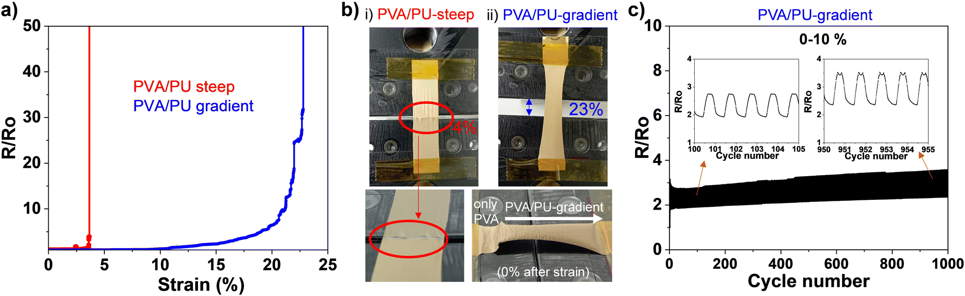 | ||
| Fig. 3 (a) Normalized resistance measured in situ during continuously increasing strain. (b) Photos of (i) PVA/PU-steep at the moment of break, 4% strain, and (ii) PVA/PU-gradient at the moment of break, 23% strain, and back at 0%. (c) Normalized resistance measured in situ during 1000 bending cycles 0–10%. Inset: Zoom in a few cycles, in the beginning, and at the end of the test. | ||
3.4 Skin impedance measurements
The application of PVA/PU-gradient nanomesh on the skin was further investigated, and a hybrid approach was developed using conductive yarns for bridging e-skin and e-textile applications. In recent examples, such functional yarns have been utilized in smart e-textiles as soft interconnections, replacing rigid, soldered, un-washable plastic insulated wires.54 In the present study, sewing conductive yarn to PVA/PU-gradient nanomesh was achieved, and the electrodes could be successfully attached to the skin after dissolving the PVA layer with water. An example is shown in the photo in Fig. 4a: the yarns were sewn onto the thickest edge of the gradient electrodes applied to the wrist, connecting them with a wristband, whose logo was made using embroidery. Moreover, skin impedance measurements on the wrist were conducted using: (i) nanomesh electrodes with interconnector and rigid wires, (ii) gradient nanomesh electrodes with conductive yarn, and (iii) commercial Ag/AgCl gel electrodes with rigid wires. The electrodes were cut so that the conductive parts in direct contact with the skin are the same size, and the cross-sections of the two nanomesh-based electrodes are presented schematically in Fig. 4b. The results of skin impedance during frequency scanning (ranging from 50 Hz to 5 MHz, repeated 3 times for each electrode) are shown in Fig. 4c. All electrodes demonstrated a similar trend, with skin impedance decreasing at higher frequencies as previously reported.9 The nanomesh-based electrodes had similar values, both higher compared to gel electrodes at low frequencies, below 1 kΩ. For better comparison, the skin measurements by the nanomesh-based electrodes were performed simultaneously with an electrode pair attached to the left wrist and the other on the right. The skin impedance was monitored for 30 min, at 1 kHz (lower frequency for biopotential monitoring), with the subject at calm (Fig. 4d). The impedance values recorded by PVA/PU-gradient with conductive yarns demonstrated a very similar evolution compared to PVA nanomesh with rigid wires. The difference in absolute values can be attributed to the higher resistance of the conductive yarns compared to the rigid wires, as well as differences between the skin sites on the left and right wrist. Thanks to the versatile thickness gradient interconnection, the nanomesh skin electrodes can be directly connected to conductive textiles and successfully record skin electrical properties. | ||
| Fig. 4 (a) Photo of gradient nanomesh electrodes with conductive yarn sewn and connected to a wristband, where the yarn logo is fabricated by embroidery, (b) cross-section schematic representation of the nanomesh-based electrodes: (i) nanomesh with interconnector and rigid wires, (ii) gradient nanomesh with conductive yarn, (c) comparison of skin impedance measurements by 3 different pairs of electrodes, during frequency scanning ×3 times (at calm), (d) comparison of skin impedance measured simultaneously with nanomesh and gradient nanomesh pairs of electrodes, left and right wrist respectively (at 1 kHz, at calm). | ||
While this study demonstrates the feasibility of conductive yarn integration, the sewing method was performed manually as a proof-of-concept. Additionally, conductive yarns attached to PU nanofiber mats may be susceptible to mechanical damage if subjected to excessive stress, such as abrupt pulling. Future work could explore an embroidery-like hemming approach using ultra-thin conductive threads at the connection with the PU-thick edge, followed by the integration of thicker conductive yarns as part of the wearable textile, similar to textile reinforcement techniques. Furthermore, previous studies have demonstrated the long-term stability of nanomesh-based electrodes, confirming their ability to maintain stable electrical performance over extended wear durations in real-world conditions, including prolonged exposure to biological fluids, high humidity and friction conditions.23,55,56 The thickness-gradient concept introduced in this study could further enhance these properties by improving interfacial mechanical stability and adhesion. This concept could be further explored in other ultra-conformal bioelectronic interfaces, such as soft ionic conductors and graphene-based e-tattoos, to introduce seamless interconnections in next-generation wearable electronics.20,27,32,33,57
4. Conclusions
In this study, we demonstrated the fabrication of a novel thickness-gradient nanomesh electrode aimed at eliminating the sharp interface between the skin electrodes and the interconnecting layers. Our approach involved the development of a 2-in-1 skin electrode-interconnector structure using a simple engineering method: successive electrospinning deposition of different nanofiber layers while adjusting the spinneret position accordingly. The proof-of-concept of the smooth gradient and its quantitative assessment were achieved through optical transmittance and scanning electron microscopy. Notably, the gradient nanomesh demonstrated enhanced mechanical durability, withstanding strain up to 23%, and exhibited stable electrical performance throughout 1000 continuous strain cycles. Moreover, rigid wires were replaced with conductive yarn sewn onto the gradient nanomesh, enabling accurate measurements of skin impedance. The feasibility of connecting directly an ultra-thin, skin-conformable electrode with a conductive textile demonstrates the potential for hybrid e-skin/e-textile devices. While this study highlights the benefits of a continuous thickness-gradient transition, some challenges remain, such as refining the gradient geometry to further enhance mechanical compliance and electrical stability. Additionally, applying this concept to highly elastic nanofiber materials could improve adaptability for more stretchable e-skin electrodes. The integration of conductive yarns, while demonstrating a promising step toward seamless textile connections, could also be further optimized to enhance durability and electrical contact. Future work may focus on improving the sewing technique to ensure long-term stability in textile-based wearable applications. Other directions may include adjusting electrospinning parameters to fine-tune the gradient's geometry and conducting simulations to better understand the strain stress distribution. The versatile concept of thickness gradient can be further expanded to other materials and adapted to address various interface issues in wearable electronic devices.Data availability
Data related to this work are presented in the main manuscript and the ESI.† Additional relevant data are available from the corresponding author upon reasonable request.Conflicts of interest
There are no conflicts to declare.Acknowledgements
D. T. P. acknowledges the Japan Society for the Promotion of Science (JSPS) for the Postdoctoral Fellowship for Research in Japan (Standard). This work was supported by the JST, CREST Grant Number JPMJCR21P2.References
- Y. Abe and M. Nishizawa, APL Bioeng., 2021, 5, 041509 CrossRef CAS PubMed.
- S. Ba and X. Hu, Comput. Educ., 2023, 200, 104797 CrossRef.
- M. R. Baidillah, R. Riyanto, P. Busono, S. Karim, R. Febryarto, A. Astasari, D. Sangaji and W. P. Taruno, Measurement, 2024, 226, 114111 CrossRef.
- T. Stuart, J. Hanna and P. Gutruf, APL Bioeng., 2022, 6, 021502 CrossRef PubMed.
- C. Tronstad, M. Amini, D. R. Bach and Ø. G. Martinsen, Physiol. Meas., 2022, 43, 02TR01 CrossRef PubMed.
- M. Babu, Z. Lautman, X. Lin, M. H. B. Sobota and M. P. Snyder, Annu. Rev. Med., 2024, 75(1), 401–415 CrossRef CAS PubMed.
- C. Xu, Y. Song, J. R. Sempionatto, S. A. Solomon, Y. Yu, H. Y. Y. Nyein, R. Y. Tay, J. Li, W. Heng, J. Min, A. Lao, T. K. Hsiai, J. A. Sumner and W. Gao, Nat. Electron., 2024, 7(2), 168–179 CrossRef CAS PubMed.
- W. Gao, S. Emaminejad, H. Y. Y. Nyein, S. Challa, K. Chen, A. Peck, H. M. Fahad, H. Ota, H. Shiraki, D. Kiriya, D.-H. Lien, G. A. Brooks, R. W. Davis and A. Javey, Nature, 2016, 529, 509–514 CrossRef CAS PubMed.
- R. Matsukawa, A. Miyamoto, T. Yokota and T. Someya, Adv. Healthcare Mater., 2020, 9, 2001322 CrossRef CAS PubMed.
- W. Sun, Z. Guo, Z. Yang, Y. Wu, W. Lan, Y. Liao, X. Wu and Y. Liu, Sensors, 2022, 22, 7784 CrossRef CAS PubMed.
- X. Nan, X. Wang, T. Kang, J. Zhang, L. Dong, J. Dong, P. Xia and D. Wei, Micromachines, 2022, 13, 1395 CrossRef PubMed.
- A. Koh, D. Kang, Y. Xue, S. Lee, R. M. Pielak, J. Kim, T. Hwang, S. Min, A. Banks, P. Bastien, M. C. Manco, L. Wang, K. R. Ammann, K.-I. Jang, P. Won, S. Han, R. Ghaffari, U. Paik, M. J. Slepian, G. Balooch, Y. Huang and J. A. Rogers, Sci. Transl. Med., 2016, 8, 366 CrossRef PubMed.
- I. You, D. G. Mackanic, N. Matsuhisa, J. Kang, J. Kwon, L. Beker, J. Mun, W. Suh, T. Y. Kim, J. B.-H. Tok, Z. Bao and U. Jeong, Science, 2020, 370, 961–965 CrossRef CAS PubMed.
- Y. Wang, H. Haick, S. Guo, C. Wang, S. Lee, T. Yokota and T. Someya, Chem. Soc. Rev., 2022, 51, 3759–3793 RSC.
- S. Gong, Y. Lu, J. Yin, A. Levin and W. Cheng, Chem. Rev., 2024, 124(2), 455–553 CrossRef CAS PubMed.
- D.-H. Kim, N. Lu, R. Ma, Y.-S. Kim, R.-H. Kim, S. Wang, J. Wu, S. M. Won, H. Tao, A. Islam, K. J. Yu, T. Kim, R. Chowdhury, M. Ying, L. Xu, M. Li, H.-J. Chung, H. Keum, M. McCormick, P. Liu, Y.-W. Zhang, F. G. Omenetto, Y. Huang, T. Coleman and J. A. Rogers, Science, 2011, 333, 838–843 CrossRef CAS PubMed.
- J. J. Kim, Y. Wang, H. Wang, S. Lee, T. Yokota and T. Someya, Adv. Funct. Mater., 2021, 31, 2009602 CrossRef CAS.
- F. Ershad, S. Patel and C. Yu, npj Flex Electron., 2023, 7, 32 CrossRef CAS PubMed.
- J. Yang, Z. Zhang, P. Zhou, Y. Zhang, Y. Liu, Y. Xu, Y. Gu, S. Qin, H. Haick and Y. Wang, Nanoscale, 2023, 15, 3051–3078 RSC.
- W. Niu, Q. Tian, Z. Liu and X. Liu, Adv. Mater., 2023, 35, 2304157 CrossRef CAS PubMed.
- A. Miyamoto, S. Lee, N. F. Cooray, S. Lee, M. Mori, N. Matsuhisa, H. Jin, L. Yoda, T. Yokota, A. Itoh, M. Sekino, H. Kawasaki, T. Ebihara, M. Amagai and T. Someya, Nat. Nanotechnol., 2017, 12, 907–913 CrossRef CAS PubMed.
- A. Miyamoto, H. Kawasaki, S. Lee, T. Yokota, M. Amagai and T. Someya, Adv. Healthcare Mater., 2022, 11, 2102425 CrossRef CAS PubMed.
- S. Harimurti, W. Wang, K. Sasaki, C. Okuda, T. Jonathan Wijaya, M. Osman Goni Nayeem, S. Lee, T. Yokota and T. Someya, Mater. Today, 2024, S1369702124000476 Search PubMed.
- S. Gashi, E. Di Lascio, B. Stancu, V. D. Swain, V. Mishra, M. Gjoreski and S. Santini, Proc. ACM Interact. Mob. Wearable Ubiquitous Technol., 2020, 4, 1–31 CrossRef.
- S. Kalasin and W. Surareungchai, Anal. Chem., 2023, 95, 1773–1784 CrossRef CAS PubMed.
- C. Wang, T. He, H. Zhou, Z. Zhang and C. Lee, Bioelectron. Med., 2023, 9, 17 CrossRef PubMed.
- H. Jang, K. Sel, E. Kim, S. Kim, X. Yang, S. Kang, K.-H. Ha, R. Wang, Y. Rao, R. Jafari and N. Lu, Nat. Commun., 2022, 13, 6604 CrossRef CAS PubMed.
- P. Mao, H. Li and Z. Yu, Sensors, 2023, 23, 3673 CrossRef CAS PubMed.
- M. Mariello, K. Kim, K. Wu, S. P. Lacour and Y. Leterrier, Adv. Mater., 2022, 34, 2201129 CrossRef CAS PubMed.
- Y. Luo, M. R. Abidian, J.-H. Ahn, D. Akinwande, A. M. Andrews, M. Antonietti, Z. Bao, M. Berggren, C. A. Berkey, C. J. Bettinger, J. Chen, P. Chen, W. Cheng, X. Cheng, S.-J. Choi, A. Chortos, C. Dagdeviren, R. H. Dauskardt, C. Di, M. D. Dickey, X. Duan, A. Facchetti, Z. Fan, Y. Fang, J. Feng, X. Feng, H. Gao, W. Gao, X. Gong, C. F. Guo, X. Guo, M. C. Hartel, Z. He, J. S. Ho, Y. Hu, Q. Huang, Y. Huang, F. Huo, M. M. Hussain, A. Javey, U. Jeong, C. Jiang, X. Jiang, J. Kang, D. Karnaushenko, A. Khademhosseini, D.-H. Kim, I.-D. Kim, D. Kireev, L. Kong, C. Lee, N.-E. Lee, P. S. Lee, T.-W. Lee, F. Li, J. Li, C. Liang, C. T. Lim, Y. Lin, D. J. Lipomi, J. Liu, K. Liu, N. Liu, R. Liu, Y. Liu, Y. Liu, Z. Liu, Z. Liu, X. J. Loh, N. Lu, Z. Lv, S. Magdassi, G. G. Malliaras, N. Matsuhisa, A. Nathan, S. Niu, J. Pan, C. Pang, Q. Pei, H. Peng, D. Qi, H. Ren, J. A. Rogers, A. Rowe, O. G. Schmidt, T. Sekitani, D.-G. Seo, G. Shen, X. Sheng, Q. Shi, T. Someya, Y. Song, E. Stavrinidou, M. Su, X. Sun, K. Takei, X.-M. Tao, B. C. K. Tee, A. V.-Y. Thean, T. Q. Trung, C. Wan, H. Wang, J. Wang, M. Wang, S. Wang, T. Wang, Z. L. Wang, P. S. Weiss, H. Wen, S. Xu, T. Xu, H. Yan, X. Yan, H. Yang, L. Yang, S. Yang, L. Yin, C. Yu, G. Yu, J. Yu, S.-H. Yu, X. Yu, E. Zamburg, H. Zhang, X. Zhang, X. Zhang, X. Zhang, Y. Zhang, Y. Zhang, S. Zhao, X. Zhao, Y. Zheng, Y.-Q. Zheng, Z. Zheng, T. Zhou, B. Zhu, M. Zhu, R. Zhu, Y. Zhu, Y. Zhu, G. Zou and X. Chen, ACS Nano, 2023, 17, 5211–5295 CrossRef CAS PubMed.
- F. Ershad, M. Houston, S. Patel, L. Contreras, B. Koirala, Y. Lu, Z. Rao, Y. Liu, N. Dias, A. Haces-Garcia, W. Zhu, Y. Zhang and C. Yu, PNAS Nexus, 2023, 2, pgac291 CrossRef PubMed.
- H. Li, P. Tan, Y. Rao, S. Bhattacharya, Z. Wang, S. Kim, S. Gangopadhyay, H. Shi, M. Jankovic, H. Huh, Z. Li, P. Maharjan, J. Wells, H. Jeong, Y. Jia and N. Lu, Chem. Rev., 2024, 124, 3220–3283 CrossRef CAS PubMed.
- S. Lee, X. Liang, J. S. Kim, T. Yokota, K. Fukuda and T. Someya, Chem. Rev., 2024, 124, 6543–6591 CrossRef CAS PubMed.
- S. Lee, D. Sasaki, D. Kim, M. Mori, T. Yokota, H. Lee, S. Park, K. Fukuda, M. Sekino, K. Matsuura, T. Shimizu and T. Someya, Nat. Nanotechnol., 2019, 14, 156–160 CrossRef CAS PubMed.
- W. Wang, M. O. G. Nayeem, H. Wang, C. Wang, J. J. Kim, B. Wang, S. Lee, T. Yokota and T. Someya, Adv. Mater. Technol., 2022, 7, 2200479 CrossRef CAS.
- C. Okutani, T. Yokota and T. Someya, ACS Appl. Nano Mater., 2020, 3, 1848–1854 CrossRef CAS.
- D. Ji, Y. Lin, X. Guo, B. Ramasubramanian, R. Wang, N. Radacsi, R. Jose, X. Qin and S. Ramakrishna, Nat. Rev. Methods Primers, 2024, 4, 1 CrossRef CAS.
- Y. Si, S. Shi and J. Hu, Nano Today, 2023, 48, 101723 CrossRef.
- A. Nadaf, A. Gupta, N. Hasan, Fauziya, S. Ahmad, P. Kesharwani and F. J. Ahmad, RSC Adv., 2022, 12, 23808–23828 RSC.
- A. Keirouz, Z. Wang, V. S. Reddy, Z. K. Nagy, P. Vass, M. Buzgo, S. Ramakrishna and N. Radacsi, Adv. Mater. Technol., 2023, 8, 2201723 CrossRef CAS.
- A. P. Kishan and E. M. Cosgriff-Hernandez, J. Biomed. Mater. Res., 2017, 105, 2892–2905 CrossRef CAS PubMed.
- C. Niu, J. Meng, X. Wang, C. Han, M. Yan, K. Zhao, X. Xu, W. Ren, Y. Zhao, L. Xu, Q. Zhang, D. Zhao and L. Mai, Nat. Commun., 2015, 6, 7402 CrossRef PubMed.
- X. Zhang, X. Gao, L. Jiang and J. Qin, Langmuir, 2012, 28, 10026–10032 CrossRef CAS PubMed.
- M. Ramalingam, M. F. Young, V. Thomas, L. Sun, L. C. Chow, C. K. Tison, K. Chatterjee, W. C. Miles and C. G. Simon, J. Biomater. Appl., 2013, 27, 695–705 CrossRef PubMed.
- H. G. Sundararaghavan and J. A. Burdick, Biomacromolecules, 2011, 12, 2344–2350 CrossRef CAS PubMed.
- T. Wu, C. Huang, D. Li, A. Yin, W. Liu, J. Wang, J. Chen, H. EI-Hamshary, S. S. Al-Deyab and X. Mo, Colloids Surf., B, 2015, 133, 179–188 CrossRef CAS PubMed.
- L. M. Ott, T. A. Zabel, N. K. Walker, A. L. Farris, J. T. Chakroff, D. G. Ohst, J. K. Johnson, S. H. Gehrke, R. A. Weatherly and M. S. Detamore, Biomed. Mater., 2016, 11, 025020 CrossRef PubMed.
- J. He, T. Qin, Y. Liu, X. Li, D. Li and Z. Jin, Mater. Lett., 2014, 137, 393–397 CrossRef CAS.
- Q. Shen, Y. Jiang, S. Guo, L. Huang, H. Xie and L. Li, J. Membr. Sci., 2022, 644, 120091 CrossRef CAS.
- J. Kim, B. G. Im, G. Jin and J.-H. Jang, ACS Appl. Mater. Interfaces, 2016, 8, 22721–22731 CrossRef CAS PubMed.
- N. Joy, R. Anuraj, A. Viravalli, H. N. Dixit and S. Samavedi, Chem. Eng. Sci., 2021, 230, 116200 CrossRef CAS.
- J. Wang and L. Ye, Composites, Part B, 2015, 69, 389–396 CrossRef CAS.
- Y. Guo, J. Drum, C. Qu and M. Cakmak, Polym. Compos., 2016, 37, 709–717 CrossRef CAS.
- R. R. Ruckdashel, N. Khadse and J. H. Park, Sensors, 2022, 22, 6055 CrossRef PubMed.
- W. Wang, S. Harimurti, D. Inoue, M. O. G. Nayeem, J. Wang, C. Okuda, D. Hashizume, S. Lee, K. Fukuda, T. Yokota and T. Someya, ACS Appl. Mater. Interfaces, 2024, 16, 27065–27074 CrossRef CAS PubMed.
- S. Lee, J. S. Kim, Y. Wang, Y. Tagawa, W. Wang, L. Sun, X. Liang, M. O. Goni Nayeem, T. Yokota, K. Fukuda and T. Someya, Device, 2025, 3, 100559 CrossRef.
- S. Zhuo, A. Tessier, M. Arefi, A. Zhang, C. Williams and S. K. Ameri, npj Flex Electron., 2024, 8, 49 CrossRef.
Footnote |
| † Electronic supplementary information (ESI) available. See DOI: https://doi.org/10.1039/d5mh00181a |
| This journal is © The Royal Society of Chemistry 2025 |