
 Open Access Article
 This Open Access Article is licensed under a
 Creative Commons Attribution 3.0 Unported Licence
Layer-dependent Schottky contact at TaX2–BY (X = S, Se, Te; Y = P, As, Sb) van der Waals interfaces
Israr
Ul Haq
a,
A.
Mustaqeem
a,
B.
Ali
a,
M.
Umair Ashraf
b,
U.
Khan
a,
Muhammad
Idrees
 c,
M.
Shafiq
a,
Yousef Mohammed
Alanazi
d and
B.
Amin
*a
c,
M.
Shafiq
a,
Yousef Mohammed
Alanazi
d and
B.
Amin
*a
aDepartment of Physics, Abbottabad University of Science & Technology, Abbottabad 22010, Pakistan. E-mail: binukhn@gmail.com; Tel: +92-333-943-665
bInstitute for Applied Physics, Department of Physics, University of Science and Technology Beijing, Beijing 100083, China
cSchool of Physics and Electronic Engineering, Jiangsu University, Zhenjiang 212013, Jiangsu, China
dCollege of Engineering, Department of Chemical Engineering, King Saud University Riyadh, Saudi Arabia
First published on 27th November 2024
Abstract
The mechanical, thermal and dynamical stabilities, electronic structure, contact type, and height of the barrier at the interface of TaX2 (X = S, Se, Te) and BY (Y = P, As, Sb) metal–semiconductor (MS) contact are investigated via first principles calculations. Binding energies, mechanical properties, phonon spectra and ab initio molecular dynamics (AIMD) simulations confirm the stabilities of these systems. TaX2–BY (X = S, Se, Te; Y = P, As, Sb) MS van der Waals heterostructures (vdWHs) are found to be metal with a Schottky contact at the interface. Formation of the n-type Schottky contact at the interface of TaX2–BY (X = S, Se, Te; Y = P, As, Sb) MS vdWHs favors electron conduction over hole conduction. Small (higher) effective mass (carrier mobility) make TaS2–BSb, TaSe2–BSb and TaTe2–BSb MS vdWHs, potential candidates for high speed nanoelectronic applications. Bader charge analysis shows that at the interface of TaX2–BY (X = S, Se, Te; Y = P, As, Sb) MS vdWHs, in TaX2 (BP, BAs) the electrons transfer from the TaX2 layer to the BP and BAs layer, while in TaX2 (BSb) the electrons transfer from the BSb layer to TaX2 layer.
1. Introduction
After the successful development of graphene in 2004,1 researchers isolated and studied more than a dozen 2D materials within less than a decade.2 Therefore, the family of 2D materials extended from the carbon materials (graphene) to transition metal dichalcogenides (TMDCs),3 MXene,4 layered metal oxides5 and many more6 with insulating,7 semiconducting,8 semimetallic,9 metallic10 and superconducting nature.11 The significant interest in 2D materials is attributed to their special physical characteristics that emerge via confinement of the transport of heat and charge to a plane.12 The unique physical characteristics are expected to make a significant impact across various applications,13 spanning from high-performance sensors,14 storage,15 catalysis,16 inert coating,17 electronic,18 optoelectronic19 and spintronic20 devices. In the family of 2D materials, TMDCs with MX2 (M = transition metal atom, X = chalcogen atom) general formula are of particular importance, where weak van der Waals (vdW) forces hold these layers together, allowing for their easy extraction from the bulk.21 The simplicity of their preparation and diverse range of characteristics, make them noteworthy in the realm of 2D materials.22 Similarly, another class of 2D materials based on group III–V semiconductors has been explored both theoretically23,24 and experimentally.25,26 The direct band gap and hexagonal lattice structure, identical to graphene, render these materials promising for the next generation of nano27 and optoelectronic device28 applications.The physical properties of the aforementioned 2D materials come with several key challenges29 such as scalability, the production of high-quality materials with large surface area, and high cost. Current synthesis methods, like chemical vapor deposition (CVD), can be expensive and complex. Stability and durability of some 2D materials can be chemically reactive or sensitive to environmental factors such as air and moisture, which can degrade their properties over time.30,31 Therefore, controlling the electronic properties and band gap of 2D materials is crucial, while some 2D materials are natural semiconductors, others, like graphene, require engineering to open a band gap for specific applications. Consequently, researchers have focused on the tuning of these materials via several techniques,32,33 for their useful device applications.19 In these techniques, stacking of 2D materials in the form of van der Waals heterostructures (vdWHs)34 provides a flexible platform for exploring novel phenomena in the design of nanoelectronic devices.35 Numerous vdWHs, particularly those in the form of semiconductor–semiconductor (SS) contact, have been extensively studied both theoretically36,37 and experimentally38,39 for their promising and remarkable applications in the field of optoelectronic devices.40 The Schottky barrier (SB) in the metal and semiconductor (MS) vdWHs minimizes resistance at contact, hence tuning (enhancing) the polarity (selectivity) of carriers in the transistor channel (photovoltaic cells), therefore, playing a crucial role in devices.41,42 These contacts (SS and MS) are fabricated via ultra-thin and flat surfaces without defects and with outstanding chemical (mechanical) stability (flexibility).43
Although, TMDCs have already been used in almost every MS contact,44–50 a significant gap exists regarding the exploration of 2D TaX2 (X = S, Se, Te) and BY (Y = P, As, Sb) MS contact. Therefore, in the present work, we have focused on the modelling of TaX2–BY MS vdWHs. Structural stability, electronic structure, contact type and height of the barrier of the modelled heterostructures are investigated, with the goal of exploring the potential applications of these materials in device fabrications.
2. Computational details
We used density functional theory (DFT) with the PWSCF code51 with generalized gradient approximation (GGA) in the Perdew–Burke–Ernzerhof (PBE) style.52 We fixed the convergence criteria for force to 10−3 Å−1 and energy to 10−5 eV for the optimization/relaxation of the lattice constant/atomic positions. We also fixed the cut-off energy to 800 eV and used a 16 × 16 × 1 k-grid for the Brillouin zone integration. To mitigate interactions between neighbouring layers of atoms, we set a vacuum layer with a thickness of 25 Å.Mechanical stability of these systems are examined using the energy-strain method in the VASPKIT code53 and visualized with the ELATE software.54 Thermal (dynamical) stabilities were investigated via AIMD (phonon) simulation (calculations).55,56 In the case of thermal stability, ab initio molecular dynamics (AIMD) simulations,55 through the Nose thermostat algorithm at a temperature of 300 K for a total of 6 ps with a time interval of 1 fs are performed. For dynamical stability, we used a 3 × 3 × 1 supercell consisting of 45 atoms. We have also used density functional perturbation theory (DFPT) with the VASP code57 to determine the harmonic second-order interatomic force constants (IFCs). In addition, we employed the PHONOPY code58 to calculate the phonon dispersion using the frozen phonon approximation.
Type (height) of the Schottky contact (barrier) is obtained using first principles calculations59 using ΦBn = ECBM − EF and ΦBp = EF − EVBM, where ECBM and EVBM are the energies of the band edges of the semiconducting material and EF is the Fermi level of the metallic material. Type (n and p) of the Schottky barrier without ΔV were also calculated60 using the Schottky–Mott rule; ϕBn = ϕ(metallic-monolayer) − χ(MS-vdWH) and ϕBp = I(MS-vdWH) − ϕ(metallic-monolayer), here ϕ, χ, and I are the work function, electron affinity, and ionization energy, respectively, of the MS vdWHs and corresponding monolayers. Band bending was calculated61 using Δϕ = ϕ(metallic-monolayer) − ϕ(semiconducting-monolayer), where ϕ(metallic-monolayer) and ϕ(semiconducting-monolayer) denote the work function of the corresponding metallic and semiconducting monolayers, respectively, in the MS vdWHs.
3. Results and discussion
Although, monolayers of TaX2 (X = S, Se, Te) and BY (Y = P, As, Sb) have already been investigated in detail in ref. 62 and 63. To verify our present approach, we have further calculated the electronic band structure of TaX2 (X = S, Se, Te) and BY (Y = P, As, Sb). In agreement with ref. 62 and 63, TaX2(BY) monolayers exhibit a metallic (direct bandgap semiconducting) nature (see Fig. 1).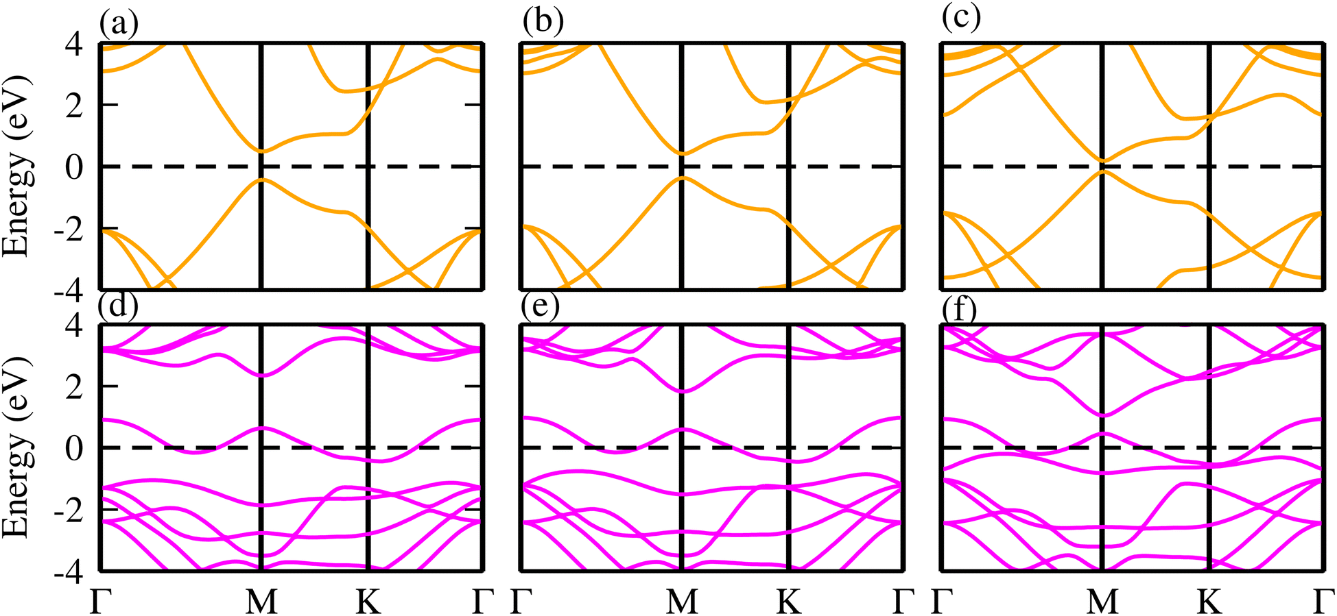 | ||
| Fig. 1 Electronic band structures of (a) BP, (b) BAs, (c) BSb, (d) TaS2, (e) TaSe2 and (f) TaTe2 monolayers. | ||
Therefore, using the optimized lattice constant of TaX2 (X = S, Se, Te)64,65 and BY (Y = P, As, Sb),66,67 TaX2–BY MS contact in six different vdWH stacking configuration patterns are fabricated, see Fig. 2. In (a), the Ta(X) atom of the TaX2 layer is placed on top of the B(Y) atom of the BY layer. In (b), the Ta atom of the TaX2 layer is placed on top of the B atom of the BY layer, while the X(Y) atom of the TaX2(BN) layer is placed on the hexagonal centre. In (c), the X atom of the TaX2 layer is placed on top of the B atom of the BY layer, while the Ta(Y) atoms of TaX2(BY) are placed on the hexagonal centre. In (d), the Ta atom of the TaX2 layer is settled on top of the Y atom of the BY layer. In (e), the Ta atom of the TaX2 layer is stacked on top of the Y atom of the BY layer, while the X(B) atom of TaX2(BY) is placed on the hexagonal centre. In (f), the X atom of the TaX2 is settled on top of the Y atom of BY, while Ta(B) atoms are placed on the hexagonal centre.
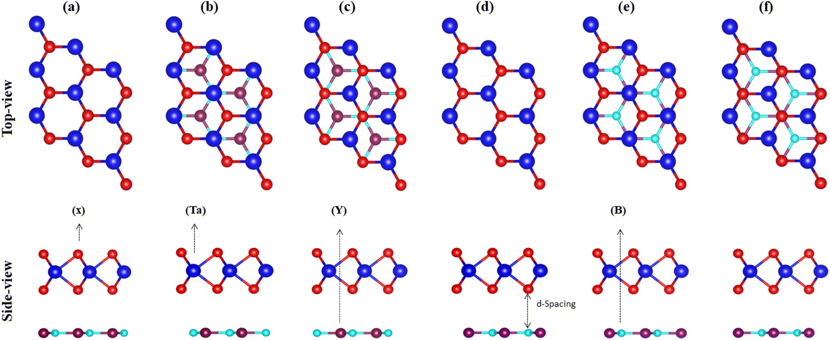 | ||
| Fig. 2 Possible stacking configurations of TaX2–BY (X = S, Se, Te; Y = P, As, Sb) MS vdWHs. | ||
Binding energy68 and the interlayer distance (d) of all six patterns of TaX2–BY MS vdWHs are calculated and presented in Table 1. Stacking (b) of TaS2–BP, (b) of TaS2–BAs, (b) of TaS2–BSb, (e) of TaSe2–BP, (b) of TaSe2–BAs, (b) of TaSe2–BSb, (e) of TaTe2–BP, (e) of TaTe2–BAs and (d) of TaTe2–BSb, are found to be the most stable stacking configurations, based on the most smaller (higher) interlayer distance (binding energies),68 see Table 1. The variation in stable stacking is due to the induced strain from the distinct chalcogen atoms and the dissimilar interface atoms. The optimized lattice constant and bond length of the most stable stacking configurations are presented in Table 2. Before considering the stable stacking configurations for further investigation, we further confirmed the stability via calculating the mechanical properties of these systems.
| TaX2–BY | TaS2–BP | TaS2–BAs | TaS2–BSb | TaSe2–BP | TaSe2–BAs | TaSe2–BSb | TaTe2–BP | TaTe2–BAs | TaTe2–BSb | |
|---|---|---|---|---|---|---|---|---|---|---|
| (a) | E b | −0.010 | −0.013 | −0.025 | −0.011 | −0.013 | −0.019 | −0.011 | −0.014 | −0.019 |
| d | 3.549 | 3.542 | 3.062 | 3.620 | 3.638 | 3.574 | 3.889 | 3.834 | 3.811 | |
| (b) | E b | −0.016 | −0.019 | −0.031 | −0.017 | −0.021 | −0.028 | −0.018 | −0.023 | −0.030 |
| d | 3.329 | 3.327 | 3.084 | 3.711 | 3.406 | 3.558 | 3.874 | 3.880 | 3.913 | |
| (c) | E b | −0.011 | −0.014 | −0.024 | −0.012 | −0.015 | −0.020 | −0.012 | −0.015 | −0.020 |
| d | 3.378 | 3.385 | 3.657 | 3.444 | 3.454 | 3.642 | 3.626 | 3.601 | 3.766 | |
| (d) | E b | −0.012 | −0.016 | −0.025 | −0.014 | −0.016 | −0.021 | −0.015 | −0.018 | −0.049 |
| d | 3.339 | 3.650 | 3.639 | 3.392 | 3.740 | 3.606 | 3.536 | 3.493 | 2.293 | |
| (e) | E b | −0.015 | −0.019 | −0.030 | −0.018 | −0.021 | −0.027 | −0.019 | −0.023 | −0.029 |
| d | 3.638 | 3.661 | 3.628 | 3.317 | 3.765 | 3.781 | 3.476 | 3.486 | 3.950 | |
| (f) | E b | −0.010 | −0.013 | −0.024 | −0.010 | −0.013 | −0.018 | −0.010 | −0.012 | −0.017 |
| d | 3.576 | 3.585 | 3.612 | 3.738 | 3.694 | 3.599 | 3.934 | 3.938 | 3.894 | |
 , ionization energy (I in eV), electron affinity (χ in eV), and band bending (ΔW in eV) of TaX2–BY (X = S, Se, Te; Y = P, As, Sb) MS vdWHs
| TaX2–BY | TaS2–BP | TaS2–BAs | TaS2–BSb | TaSe2–BP | TaSe2–BAs | TaSe2–BSb | TaTe2–BP | TaTe2–BAs | TaTe2–BSb |
|---|---|---|---|---|---|---|---|---|---|
| a | 3.26 | 3.35 | 3.51 | 3.34 | 3.43 | 3.61 | 3.46 | 3.54 | 3.72 |
| M–X | 2.46 | 2.48 | 2.52 | 2.58 | 2.60 | 2.64 | 2.79 | 2.79 | 2.78 |
| B–N | 1.88 | 1.94 | 2.08 | 1.93 | 1.98 | 2.10 | 1.99 | 2.05 | 2.32 |
| d | 3.33 | 3.33 | 3.08 | 3.32 | 3.41 | 3.56 | 3.48 | 3.49 | 2.29 |
| C 11 | 299.38 | 282.34 | 252.80 | 254.77 | 252.49 | 226.39 | 142.89 | 156.02 | 159.40 |
| C 12 | 84.46 | 82.65 | 73.65 | 79.53 | 69.60 | 64.49 | 62.46 | 72.88 | 42.81 |
| E | 275.55 | 258.15 | 231.34 | 299.95 | 233.31 | 208.02 | 115.58 | 121.98 | 147.90 |
| G | 107.46 | 99.85 | 89.57 | 87.62 | 91.45 | 80.95 | 40.21 | 41.57 | 58.29 |
| ν | 0.282 | 0.239 | 0.291 | 0.312 | 0.276 | 0.285 | 0.437 | 0.467 | 0.269 |
| ΔV | 4.93 | 2.22 | 4.88 | 7.23 | 4.41 | 2.67 | 4.74 | 1.64 | 2.53 |
| ϕ | 4.01 | 3.92 | 3.65 | 3.81 | 3.82 | 3.63 | 3.28 | 3.58 | 4.01 |
|
0.71 | 0.61 | 0.43 | 0.79 | 0.68 | 0.48 | 0.94 | 0.79 | 0.57 |

|
0.66 | 0.57 | 0.41 | 0.75 | 0.65 | 0.47 | 0.91 | 0.77 | 0.55 |
| I | 4.65 | 4.59 | 4.58 | 4.82 | 4.79 | 4.73 | 5.11 | 5.05 | 5.38 |
| χ | 4.65 | 4.58 | 4.57 | 4.81 | 4.79 | 4.70 | 5.10 | 5.04 | 5.36 |
| ΔW | 0.23 | 0.23 | 0.23 | 0.24 | 0.24 | 0.24 | 0.32 | 0.29 | 0.24 |
Mechanical stability of the most stable stacking configurations of TaX2–BY (X = S, Se, Te; Y = P, As, Sb) MS vdWH are assisted via the energy-strain method.69–71 Using the hexagonal symmetry of TaX2–BY MS vdWH, two independent elastic constants (C11 and C12), Young's modulus, shear modulus, and Poisson's ratios are calculated and presented in Table 2, that meet the Born criteria: C11 > 0, C12 > 0, and C11 > ∣C12∣.69–71 Therefore, these findings indicate the high mechanical stability of TaX2–BY (X = S, Se, Te; Y = P, As, Sb) MS vdWH, in agreement with previous reports.69–71
Thermal stability in terms of the fluctuation energy as a function of time, of the energetically most favorable stacking configurations in TaX2–BY (TaS2–BP, TaS2–BAs and TaS2–BSb), are given in Fig. 3. One can observe that in the case of TaS2–BP, TaS2–BAs and TaS2–BSb, heterostructures after 4 ps, there is no structure distortion. Moreover, through the AIMD simulation, our results demonstrate that the geometrical structure of TaS2–BP, TaS2–BAs and TaS2–BSb is retained after 4000 step simulations and the average value of the total energy remains nearly constant. All these findings demonstrate that TaS2–BP, TaS2–BAs and TaS2–BSb are thermally stable at room temperature.
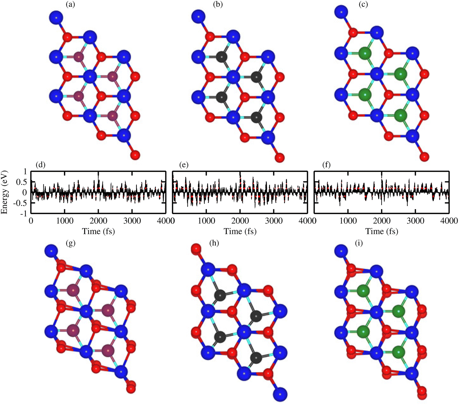 | ||
| Fig. 3 Ab initio molecular dynamics simulation of (a, d, and g) TaS2–BP, (b, e, and h) TaS2–BAs and (c, f, and i) TaS2–BSb, van der Waals heterostructures. Geometrical structure (a–c) before heating; (g–i) after heating with (d–f) fluctuating energy. | ||
The phonon dispersion curves in Fig. 4 for the TaS2–BP, TaS2–BAs, and TaS2–BSb MS vdWHs show no imaginary frequencies throughout the Brillouin zone, confirming their dynamic stability. The lack of imaginary modes indicates that the atomic arrangements reside at a local minimum on the potential energy surface, which is a key indicator of structural stability. Using the PBE functional, the electronic band structures are displayed in Fig. 5, where green (red) lines are attributed to the TaX2(BY) layers in TaX2–BY (X = S, Se, Te; Y = P, As, Sb) MS vdWHs. The electronic band structures in Fig. 5, show that all TaX2–BY (X = S, Se, Te; Y = P, As, Sb) MS vdWHs are metals with type-III band alignment72 and look like the sum of band structure of TaX2 and BY (Y = P, As, Sb) monolayers. The transition of BY (Y = P, As, Sb) to a metal is ascribed to the contribution of metallic states from TaX2 (X = S, Se, Te) monolayer, enhancing its conductivity and making it suitable for various electronic applications involving Schottky contacts.
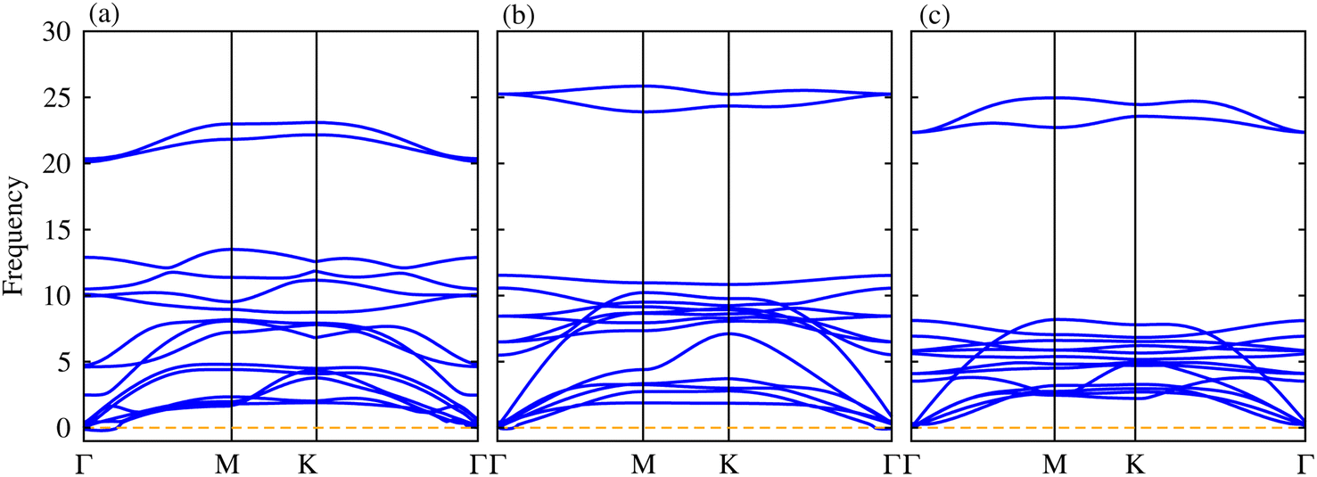 | ||
| Fig. 4 Phonon dispersion curves of (a) TaS2–BP, (b) TaS2–BAs and (c) TaS2–BSb MS vdWHs. | ||
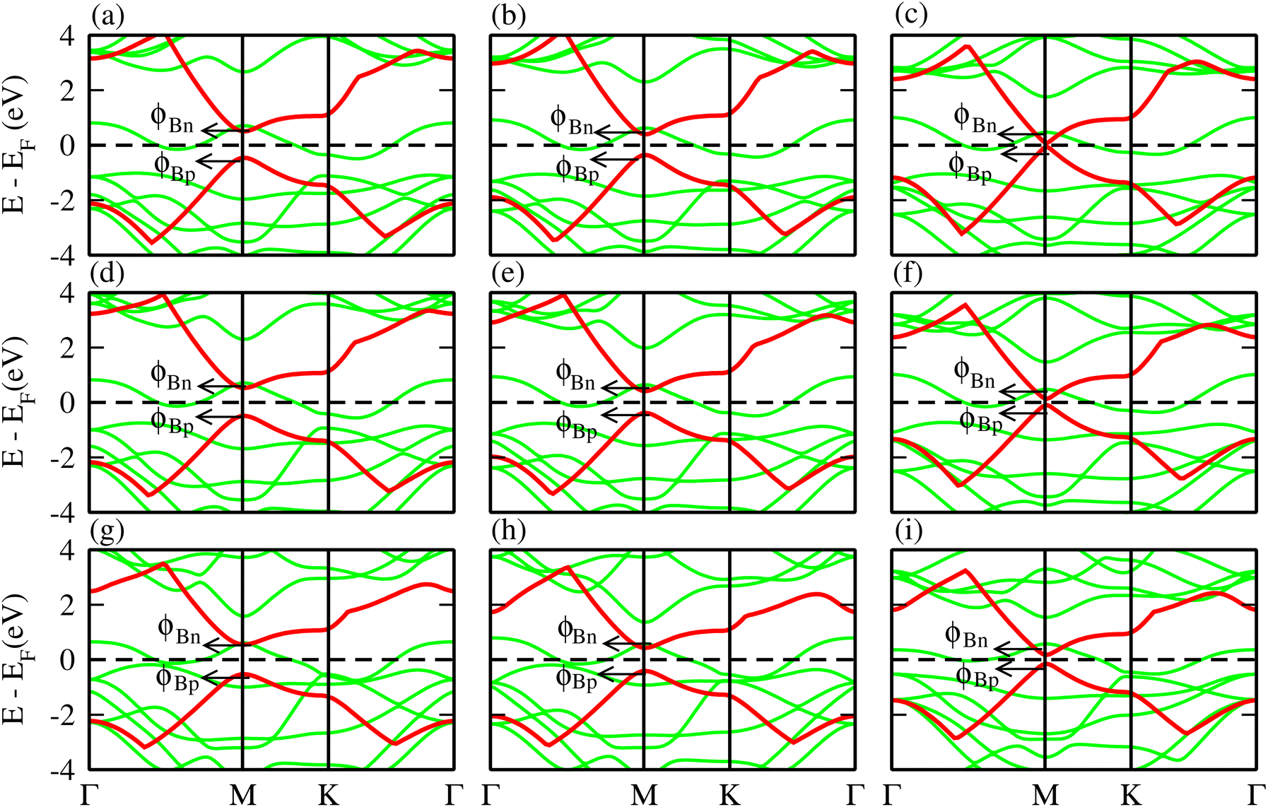 | ||
| Fig. 5 Electronic band structure of (a) TaS2–BP, (b) TaS2–BAs, (c) TaS2–BSb, (d) TaSe2–BP, (e) TaSe2–BAs, (f) TaSe2–BSb, (g) TaTe2–BP, (h) TaTe2–BAs and (i) TaTe2–BSb MS vdWHs. | ||
PDOS of the TaX2–BY MS vdWHs are presented in Fig. 6, and show that the main contributions at the Fermi level are due to the Ta-d (d3z2−r2, dxy) and (S, Se, Te)-p orbital of the TaX2 monolayers (crossing the Fermi level); while both the valence and conduction band without crossing the Fermi level, are due to the B-px and (Y = P, As, Sb)-pz orbitals of the BY monolayer. After stacking, the TaX2 monolayer shifts the conduction band minimum (CBM) of the BY layer toward the Fermi level due to the difference in electronegativity. The position of these orbitals near to the Fermi level in the valence and conduction bands show that the band structure of BY and TaX2 monolayers are well preserved in the TaX2–BY MS vdWHs. The minimum (maximum) of the conduction (valence) band is due to the Ta-d3z2r2 (Ta-dx2−y2, dxy) orbital with a very small contribution from the Ta-dx2−y2 and dxy orbitals, see Fig. 6. The B-px and py orbital dominate the valence band minimum (VBM), with a small contribution from the B-pz orbitals. Through modelling TaX2–BY MS vdWHs, we found that strain is induced in the corresponding monolayers due to the lattice mismatch, tuning the coupling between the orbitals of the TMDCs (Ta-d) and chalcogen atoms ((S, Se, Te)-p). Therefore, splitting in the bonding and antibonding states of BY monolayers in TaX2–BY MS vdWHs fluctuates, and hence the position of the contributing orbital at the Fermi level varies.
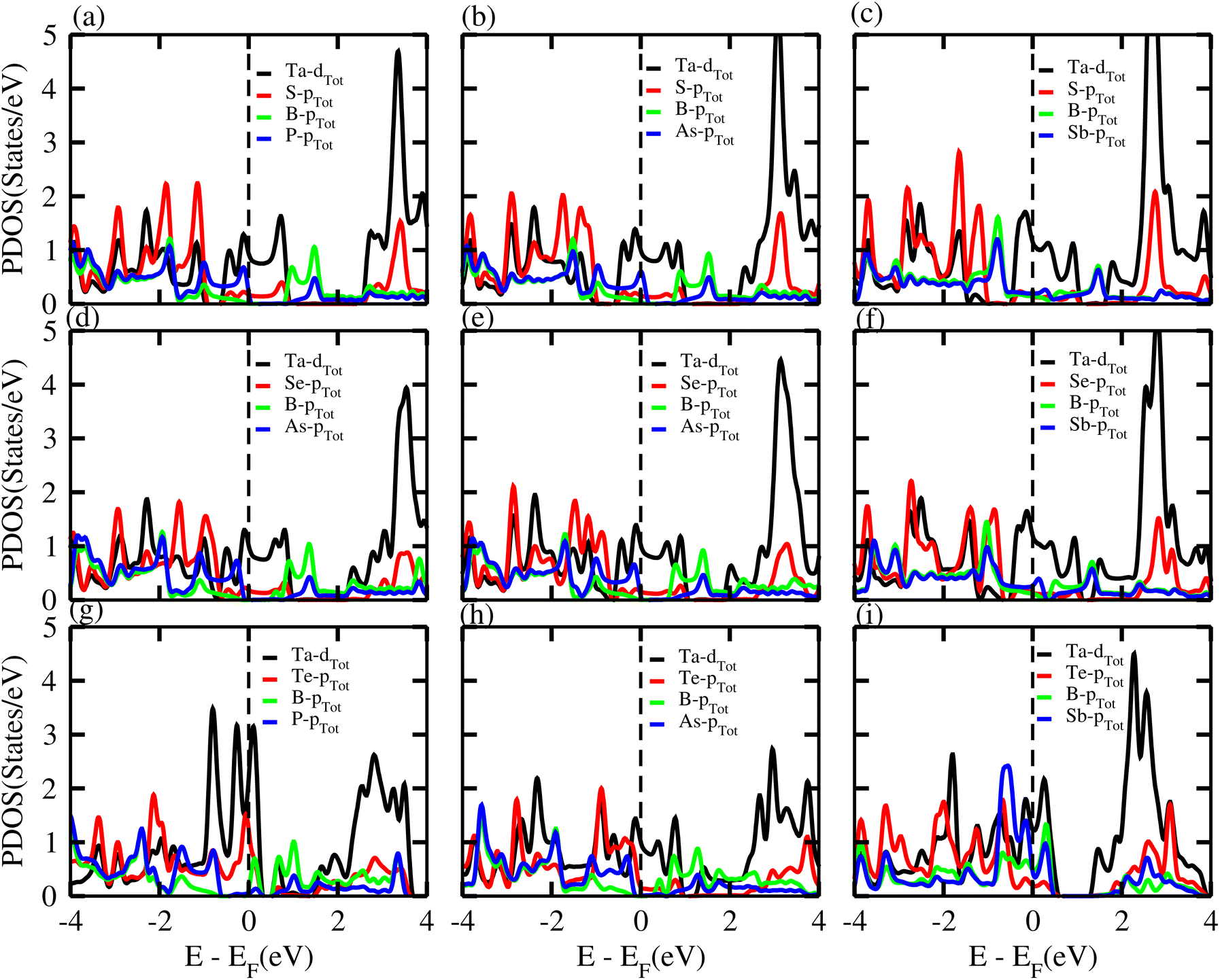 | ||
| Fig. 6 PDOS of (a) TaS2–BP, (b) TaS2–BAs, (c) TaS2–BSb, (d) TaSe2–BP, (e) TaSe2–BAs, (f) TaSe2–BSb, (g) TaTe2–BP, (h) TaTe2–BAs and (i) TaTe2–BSb, vdWHs. | ||
Furthermore, for the use of TaX2–BY (X = S, Se, Te; Y = P, As, Sb) MS vdWHs in device applications, effective mass and carrier mobility are investigated and related by μ = eτ/m*.73 Thus, to evaluate the carrier mobility of TaX2–BY MS vdWHs, effective mass is calculated using74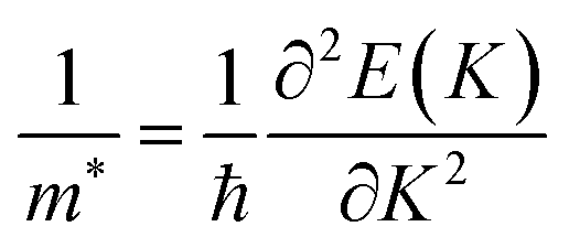 where, ℏ is Planck’s constant and K is the wave vector. Based on the above equation, using the parabolic fitting of the CB and VB of TaX2–BY MS vdWHs, the calculated effective mass for electrons (holes) are given in Table 2. Quite a small effective mass in the case of TaS2–BSb, TaSe2–BSb and TaTe2–BSb MS vdWHs, exhibit high carrier mobility, and hence show potential for efficient nanoelectronic devices.
Relative locations of the metal (TaX2) with semiconductor (BY) band edges in TaX2–BY (X = S, Se, Te; Y = P, As, Sb) MS vdWHs establish the Schottky or ohmic junctions across the interface. Tuning the Schottky barrier (SBH) can change the current flow across the interface of the TaX2–BY (X = S, Se, Te; Y = P, As, Sb) MS vdWHs, hence boosting the device performance.75,76 The band structures in Fig. 5 indicate that the Fermi level of TaX2 (metal layer) sits in the band edges of BY (semiconductor layer), and hence establish Schottky contacts77 at the interface of TaX2–BY MS vdWHs. The type of Schottky contact (n-type or p-type) is obtained using the Schottky–Mott rule,78 see computational details. The calculated values of the Schottky barrier ϕBn and ϕBp using first principles calculations and the Schottky–Mott rule, are given in Fig. 7, which shows that ϕBn of all stacking configurations is smaller than ϕBp, suggesting that they form an n-type Schottky contact. Therefore, the MS vdWHs under consideration favor electron conduction over hole conduction, and hence have significant implications in transistors, sensors, photodetectors, and other electronic components.79 It is clearly observed that the SBH increases (decreases) from P to As to Sb in TaS2–BY (TaTe2–BY) MS vdWHs. Moreover, the metallic nature of these heterostructures suppress the metal induced gap states (MIGS) in BY (Y = P, As, Sb) monolayers, hence, leading to weak Fermi Level Pinning (FLP). Weak vdW interactions redistribute the charge density at the interface, see Fig. 9 (discussed later on), and hence establish interface dipoles (ID). Therefore, neglecting the metal semiconductor interaction (without considering ΔV) should ideally follow the predictions of the Schottky–Mott rule. Therefore, type (n and p) of the Schottky barrier without ΔV were also calculated60 using ϕBn = ϕ(metallic-monolayers) − χ(vdWH) and ϕBp = I(vdWH) − ϕ(metallic-monolayers). These IDs may lead to deviation from the Schottky–Mott limit, due to shifting of the electronic levels and FLP effect at the interface from their original positions.80 The band bending of the TaX2–BY systems reveals the presence of both p-type and n-type Schottky barrier even without the transfer of charge between the corresponding monolayers. When Δϕ are greater than 0 or Δϕ is less than 0, it signifies the formation of n-type and p-type Schottky contacts.50 In the TaX2–BY vdWHs under study, Δϕ is greater than 0, see Table 2. This observation suggests that charge will preferentially flow from metal to semiconductor, indicating n-type contact due to the high values of Δϕ (greater than 0), which demonstrate that holes will flow from TaX2 to the BY layer. The controllable electronic properties and formation of the Schottky contact in TaX2–BY MS vdWHs makes it a potential candidate for Schottky nanodevices.50
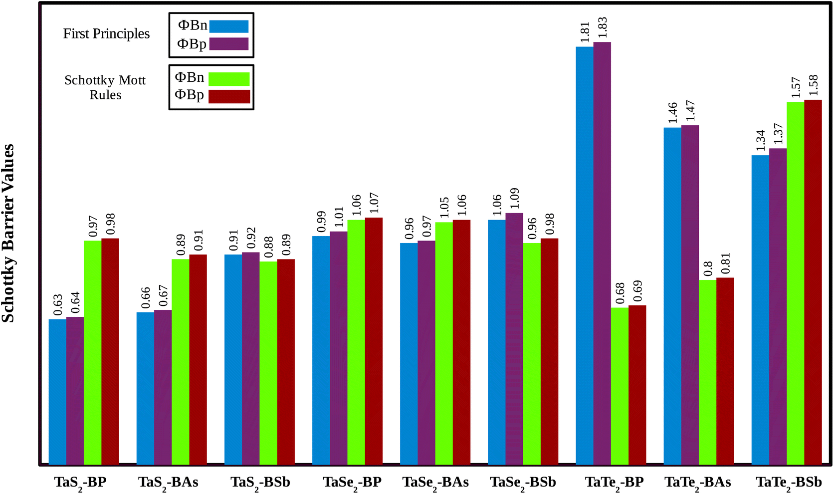 | ||
| Fig. 7 Schottky barrier height calculated using the Schottky–Mott rule and first principles calculation of TaX2 (X = S, Se, Te)–BY (Y = P, As, Sb) MS vdWHs. | ||
In the case of TaX2–BY MS vdWHs, the TaX2 (BP, BAs) layer exhibits shallower (deeper) potential confirming charge transfer from TaX2 to the BP and BAs layer. On the contrary, in the case of TaX2 (X = S, Se, Te)–BSb, the TaX2 (BSb) layer is deeper (shallower), which confirms the transfer of charge from the BSb layer to TaX2, due to the fact that BSb has a higher work function than TaX2. The calculated ΔV varies within (1.64 to 7.23 eV) due to the difference in electronegativity among the atoms81 at the interface. For both TaX2 and BY monolayers in the form of TaX2–BY MS vdWHs, the electrostatic potential effectively controls charge movement at the interface, contributing to increased energy conversion efficiency. The work function (ϕ) of TaX2–BY MS vdWHs – defined as the difference between the vacuum level and Fermi level – was calculated using average electrostatic potential as displayed in Fig. 8. ϕ predominantly depends on the condition of the material surface due to changes in surface electric field settings and electron distribution at the interface. The calculated ϕ for of TaX2–BY MS vdWHs lies in the range 3.285–4.009 eV, see Table 2, which shows the potential for field effect transistors.82
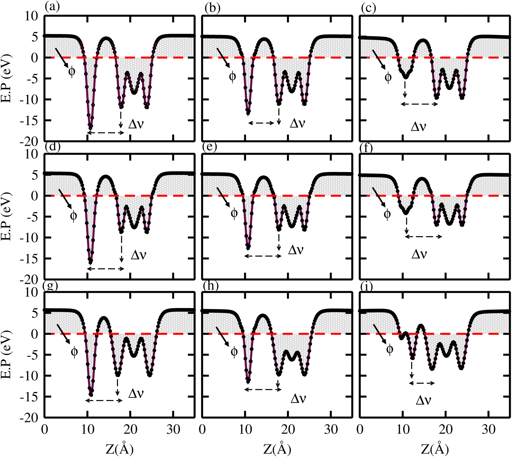 | ||
| Fig. 8 Average electrostatic potential of (a) TaS2–BP, (b) TaS2–BAs, (c) TaS2–BSb, (d) TaSe2–BP, (e) TaSe2–BAs, (f) TaSe2–BSb, (g) TaTe2–BP, (h) TaTe2–BAs, and (i) TaTe2–BSb, MS vdWHs. | ||
To see the contact charge redistribution, we have calculated the charge density difference of the TaX2–BY (X = S, Se, Te; Y = P, As, Sb) MS vdWHs using83,84 ▽ρ = ρMSvdWHs − ρmonolayer-I − ρmonolayer-II. In the case of TaX2–BY (X = S, Se, Te; Y = P, As) MS vdWHs, charge depletion (accumulation) around the TaX2 (BP) layer indicates loss (gain) of electrons in TaX2 (BP, BAs). For TaX2–BSb MS vdWHs, TaX2 (BSb) gain (loss) of electrons in this region makes an electron (hole)-rich region.85 The BSb layer becomes a depletion region with fewer electrons, resulting in a hole-rich environment, while the TaX2 layer accumulates electrons and becomes electron-rich as shown in Fig. 9. Quantitative behaviour of charge transfer, analysed via Bader charges, show a maximum of 0.065409e and minimum of 0.000399e transferred from TaX2 to the BY monolayer, see Table 3. The phenomena of the transfer of charge shows a strong interlayer coupling and vdWh interaction established at the interface of TaX2 and BY monolayers in TaX2–BN MS vdWHs. A charge transportation built-in-electric field in the interface, creates a region where charges are separated, generating an electric field at the interface86 which enhances the carrier mobility along with the number of carriers (holes and electrons). A similar result is also confirmed via experiments in graphene/GaSe![[thin space (1/6-em)]](https://www.rsc.org/images/entities/char_2009.gif) 87 and graphene/MoS2.88 Ionization potential (I); I = Evac − EVBM, for the TaX2–BY MS contact in Table 2, helps in determining the Schottky barrier height, crucial for understanding the behavior of MS contacts.
87 and graphene/MoS2.88 Ionization potential (I); I = Evac − EVBM, for the TaX2–BY MS contact in Table 2, helps in determining the Schottky barrier height, crucial for understanding the behavior of MS contacts.
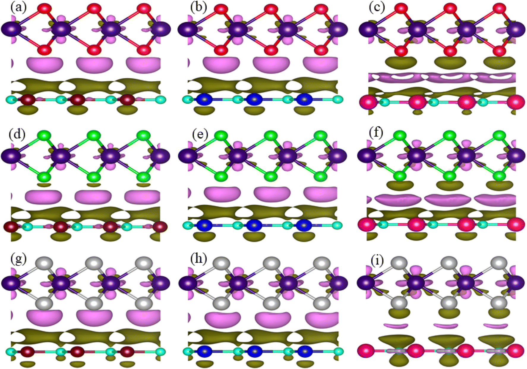 | ||
| Fig. 9 Charge density difference of (a) TaS2–BP, (b) TaS2–BAs, (c) TaS2–BSb, (d) TaSe2–BP, (e) TaSe2–BAs, (f) TaSe2–BSb, (g) TaTe2–BP, (h) TaTe2–BAs, and (i) TaTe2–BSb, MS vdWHs. | ||
| TaX2–BY | TaS2–BP | TaS2–BAs | TaS2–BSb | TaSe2–BP | TaSe2–BAs | TaSe2–BSb | TaTe2–BP | TaTe2–BAs | TaTe2–BSb |
|---|---|---|---|---|---|---|---|---|---|
| TaX2 | 0.026 (h+) | 0.038 (h+) | 0.065 (e−) | 0.013 (h+) | 0.024 (h+) | 0.050 (e−) | 0.001 (h+) | 0.008 (h+) | 0.033 (e−) |
| BY | 0.027 (e−) | 0.039 (e−) | 0.065 (h+) | 0.012 (e−) | 0.025 (e−) | 0.051 (h+) | 0.001 (e−) | 0.009 (e−) | 0.032 (h+) |
4. Conclusion
Using DFT calculations and electronic band structure, the contact (barrier) type (height) at the interface of TaX2–BY (X = S, Se, Te; Y = P, As, Sb) MS vdWHs are investigated. The stability of these systems are confirmed via binding energies, mechanical (born criteria), properties, AIMD simulation and phonon spectra calculations. Electronic band structures confirm the metallic behaviour of TaX2–BY MS vdWHs with weak vdW interactions in the corresponding monolayers. The quite small effective mass in the case of TaS2–BSb, TaSe2–BSb and TaTe2–BSb MS vdWHs, exhibit high carrier mobility and hence show potential for high speed nanoelectronic applications. n-type Schottky contact at the interface of TaX2–BY MS vdWHs favor electron conduction over hole conduction, hence has significant applications in transistors, sensors, photodetectors, and other electronic components. Large potential drop in the case of TaS2–BP, TaS2–BSb, TaSe2–BP, TaSe2–BAs and TaTe2–BP of the TaX2–BY MS vdWHs, suggests a considerable electrostatic field at the interface, which controls the charge transportation and strengthens the power conversion efficiency. Analysis of the Bader charges, show that a maximum (minimum) of 0.065409 (0.000399)e are transferred from the TaX2(BY) monolayer. The work function for the TaX2–BY MS contact lies in the 3.285–4.009 eV range, which shows potentiality for FET.Data availability
The data that support the findings of this study are available on request from the corresponding author.Conflicts of interest
There are no conflicts to declare.Acknowledgements
The authors would like to acknowledge Researcher's Supporting Project Number (RSP2024R511), King Saud University, Riyadh, Saudi Arabia. The authors also express their deep gratitude to the Jiangsu University, China, for provision of computational resources.References
- H. C. Lee, W. W. Liu, S. P. Chai, A. R. Mohamed, C. W. Lai, C. S. Khe and N. M. S. Hidayah, Procedia Chem., 2016, 19, 916921 CrossRef.
- D. Geng and H. Y. Yang, Adv. Mater., 2018, 30, 1800865 CrossRef.
- H. Li, Y. Shi, M. H. Chiu and L. J. Li, Nano Energy, 2015, 18, 293305 CrossRef.
- J. Fatima, M. B. Tahir, A. Rehman, M. Sagir, M. Rafique, M. A. Assiri and M. Alzaid, Mater. Sci. Eng., B, 2023, 289, 116230 CrossRef CAS.
- M. E. Landis, B. A. Aufdembrink, P. Chu, I. D. Johnson, G. W. Kirker and M. K. Rubin, J. Am. Chem. Soc., 1991, 113, 3189 CrossRef CAS.
- K. Khan, A. K. Tareen, M. Aslam, R. Wang, Y. Zhang, A. Mahmood and Z. Guo, J. Mater. Chem. C, 2020, 8, 387440 Search PubMed.
- A. Raza, U. Qumar, J. Hassan, M. Ikram, A. Ul-Hamid, J. Haider and S. Ali, Appl. Nanosci., 2020, 10, 3875 CrossRef CAS.
- A. Chaves, J. G. Azadani, H. Alsalman, D. R. Da Costa, R. Frisenda, A. J. Chaves and T. Low, npj 2D Mater. Appl., 2020, 4, 29 CrossRef CAS.
- L. Cao, G. Zhou, Q. Wu, S. A. Yang, H. Y. Yang, Y. S. Ang and L. K. Ang, Phys. Rev. Appl., 2020, 13, 054030 CrossRef CAS.
- W. Xu, Y. Ke, Z. Wang, W. Zhang and A. T. S. Wee, Surf. Sci. Rep., 2021, 76, 100542 CrossRef CAS.
- Y. Zhang, M. Xu, Q. Zeng, J. Hao and Y. Li, Mater. Today Electronics, 2023, 5, 100053 CrossRef.
- S. Z. Butler, S. M. Hollen, L. Cao, Y. Cui, J. A. Gupta, H. R. Gutiérrez and J. E. Goldberger, ACS Nano, 2013, 7, 2898 CrossRef CAS PubMed.
- F. R. Fan, R. Wang, H. Zhang and W. Wu, Chem. Soc. Rev., 2021, 50, 10983 RSC.
- S. Mehdi Aghaei, A. Aasi and B. Panchapakesan, ACS Omega, 2021, 6, 2450 CrossRef CAS PubMed.
- B. Anasori, M. R. Lukatskaya and Y. Gogotsi, Nat. Rev. Mater., 2017, 2, 17 Search PubMed.
- A. Gupta, T. Sakthivel and S. Seal, Prog. Mater. Sci., 2015, 73, 44126 CrossRef.
- G. Wang, P. Yang and E. R. Batista, Phys. Rev. Mater., 2020, 4, 024001 CrossRef CAS.
- N. Izyumskaya, D. O. Demchenko, V. Avrutin, Ü. Özgür and H. Morkoç, Turk. J. Phys., 2014, 38, 478496 Search PubMed.
- S. Kang, D. Lee, J. Kim, A. Capasso, H. S. Kang, J. W. Park and G. H. Lee, 2D Mater., 2020, 7, 022003 CrossRef CAS.
- Y. P. Feng, L. Shen, M. Yang, A. Wang, M. Zeng, Q. Wu and C. R. Chang, Wiley Interdiscip. Rev.:Comput. Mol. Sci., 2017, 7, e1313 Search PubMed.
- M. Zhao, Y. Hao, C. Zhang, R. Zhai, B. Liu, W. Liu and H. Li, Crystals, 2022, 12, 1087 CrossRef CAS.
- Y. C. Lin, R. Torsi, R. Younas, C. L. Hinkle, A. F. Rigosi, H. M. Hill and J. A. Robinson, ACS Nano, 2023, 17, 9694 CrossRef CAS.
- M. P. Mikhailova, K. D. Moiseev and Y. P. Yakovlev, Semiconductors, 2019, 53, 273290 Search PubMed.
- H. J. Joyce, Q. Gao, H. H. Tan, C. Jagadish, Y. Kim, J. Zou and M. B. Johnston, Prog. Quantum Electron., 2011, 35, 2375 CrossRef.
- A. K. Singh, H. L. Zhuang and R. G. Hennig, Phys. Rev. B:Condens. Matter Mater. Phys., 2014, 89, 245431 CrossRef.
- M. Buscema, J. O. Island, D. J. Groenendijk, S. I. Blanter, G. A. Steele, H. S. van der Zant and A. Castellanos-Gomez, Chem. Soc. Rev., 2015, 44, 3691 RSC.
- M. Zeng, Y. Xiao, J. Liu, K. Yang and L. Fu, Chem. Rev., 2018, 118, 6236 CrossRef CAS PubMed.
- C. Lan, Z. Shi, R. Cao, C. Li and H. Zhang, Nanoscale, 2020, 12, 11784 RSC.
- S. Yu, X. Wu, Y. Wang, X. Guo and L. Tong, Adv. Mater., 2017, 29, 1606128 CrossRef.
- S. K. Chakraborty, B. Kundu, B. Nayak, S. P. Dash and P. K. Sahoo, iScience, 2022, 25, 103942 CrossRef CAS PubMed.
- C.-L. Lo, B. A. Helfrecht, Y. He, D. M. Guzman, N. Onofrio, S. Zhang, D. Weinstein, A. Strachan and Z. Chen, J. Appl. Phys., 2020, 128, 080903 CrossRef CAS.
- A. J. Watson, W. Lu, M. H. Guimarães and M. Stöhr, 2D Mater., 2021, 8, 032001 CrossRef CAS.
- X. Wang, Y. Sun and K. Liu, 2D Mater., 2019, 6, 042001 CrossRef CAS.
- J. Qi, Z. Wu, W. Wang, K. Bao, L. Wang, J. Wu and Q. He, Int. J. Extreme Manuf., 2023, 5, 022007 CrossRef CAS.
- Z. H. Li, J. N. Han, S. G. Cao and Z. H. Zhang, Appl. Surf. Sci., 2023, 636, 157766 CrossRef CAS.
- M. K. Mohanta, A. Kishore and A. De Sarkar, Nanotechnology, 2020, 31, 495208 CrossRef CAS PubMed.
- A. Albar and S. A. Aravindh, J. Phys.: Condens. Matter, 2021, 33, 475701 CrossRef CAS PubMed.
- Q. Li, J. Meng and Z. Li, J. Mater. Chem. A, 2022, 10, 8107 RSC.
- Y. Xiong, D. Xu, Y. Feng, G. Zhang, P. Lin and X. Chen, Adv. Mater., 2023, 35, 2206939 CrossRef CAS PubMed.
- T. Su, Y. Li, Q. Wang, W. Zhao, L. Cao and Y. S. Ang, J. Phys. D: Appl. Phys., 2023, 56, 234001 CrossRef CAS.
- H. S. Nalwa, RSC Adv., 2020, 10, 30529 RSC.
- S. Li, F. Wang, Y. Wang, J. Yang, X. Wang, X. Zhan and Z. Wang, Adv. Mater., 2024, 36, 2301472 CrossRef CAS.
- R. Yang, J. Fan and M. Sun, Front. Phys., 2022, 17, 43202 CrossRef.
- C. Kim, I. Moon, D. Lee, M. S. Choi, F. Ahmed, S. Nam, Y. Cho, H.-J. Shin, S. Park and W. J. Yoo, ACS Nano, 2017, 11, 1588 CrossRef CAS PubMed.
- Y. Guo, D. Liu and J. Robertson, ACS Appl. Mater. Interfaces, 2015, 7, 25709 CrossRef CAS PubMed.
- J. Kang, W. Liu, D. Sarkar, D. Jena and K. Banerjee, Phys. Rev. X, 2014, 4, 031005 CAS.
- C. Gong, L. Colombo, R. M. Wallace and K. Cho, Nano Lett., 2014, 14, 1714 CrossRef CAS PubMed.
- H. Khan, M. U. Ashraf, M. Idrees, H. U. Din, C. V. Nguyen and B. Amin, RSC Adv., 2022, 12, 12292 RSC.
- M. U. Ashraf, H. Khan, M. Munawar, H. Ud Din, M. Idrees, M. Bilal, Y. Saeed, M. Shafiq and B. Amin, Mater. Sci. Semicond. Process., 2022, 141, 106424 CrossRef CAS.
- U. Khan, B. Ali, H. Ullah, M. Idrees, C. Nguyen and B. Amin, Micro Nanostruct., 2024, 187, 207765 CrossRef CAS.
- P. Giannozzi, S. Baroni, N. Bonini, M. Calandra, R. Car, C. Cavazzoni, D. Ceresoli, G. L. Chiarotti, M. Cococcioni, I. Dabo, A. Dal Corso, S. de Gironcoli, S. Fabris, G. Fratesi, R. Gebauer, U. Gerstmann, C. Gougoussis, A. Kokalj, M. Lazzeri, L. Martin-Samos, N. Marzari, F. Mauri, R. Mazzarello, S. Paolini, A. Pasquarello, L. Paulatto, C. Sbraccia, S. Scandolo, G. Sclauzero, A. P. Seitsonen, A. Smogunov, P. Umari and R. M. Wentzcovitch, J. Phys.: Condens. Matter, 2009, 21, 395502 CrossRef PubMed.
- J. P. Perdew, K. Burke and M. Ernzerhof, Phys. Rev. Lett., 1996, 77, 3865 CrossRef CAS.
- V. Wang, N. Xu, J. C. Liu, G. Tang and W. T. Geng, Comput. Phys. Commun., 2021, 267, 108033 CrossRef CAS.
- R. Gaillac, P. Pullumbi and F.-X. Coudert, J. Phys.: Condens. Matter, 2016, 28, 275201 CrossRef PubMed.
- R. Yuan, J. A. Napoli, C. Yan, O. Marsalek, T. E. Markland and M. D. Fayer, ACS Cent. Sci., 2019, 5, 1269 CrossRef CAS.
- O. I. Malyi, K. V. Sopiha and C. Persson, ACS Appl. Mater. Interfaces, 2019, 11, 24876 CrossRef CAS.
- G. Kresse and J. Furthmüller, Phys. Rev. B:Condens. Matter Mater. Phys., 1996, 54, 11169 CrossRef CAS PubMed.
- A. Togo, F. Oba and I. Tanaka, Phys. Rev. B:Condens. Matter Mater. Phys., 2008, 78, 134106 CrossRef.
- J. Bardeen, Phys. Rev., 1947, 71, 717 CrossRef.
- Y. Liu, P. Stradins and S.-H. Wei, Sci. Adv., 2016, 2, e1600069 CrossRef PubMed.
- B. Liu, L. Wu, Y. Q. Zhao, L. Z. Wang and M. Q. Caii, Phys. Chem. Chem. Phys., 2016, 18, 19918 RSC.
- N. Guo, X. Fan, Z. Chen, Z. Luo, Y. Hu, Y. An and S. Ma, Comput. Mater. Sci., 2020, 176, 109540 CrossRef CAS.
- M. Xie, S. Zhang, B. Cai, Z. Zhu, Y. Zou and H. Zeng, Nanoscale, 2016, 8, 13407 RSC.
- Y. Zhang, Z. Tong, A. Pecchia, C. Yam, T. Dumitric and T. Frauenheim, Nanoscale, 2022, 14, 13053 RSC.
- Y. Ding, Y. Wang, J. Ni, L. Shi, S. Shi and W. Tang, Phys. B, 2011, 406, 2254 CrossRef CAS.
- B. Onat, L. Hallioglu, S. Ipek and E. Durgun, J. Phys. Chem. C, 2017, 121, 4583 CrossRef CAS.
- H. Kolavada, D. J. Trivedi, P. N. Gajjar and S. K. Gupta, J. Energy Storage, 2023, 72, 108444 CrossRef.
- B. Amin, N. Singh and U. Schwingenschlögl, Phys. Rev. B:Condens. Matter Mater. Phys., 2015, 92, 075439 CrossRef.
- G. Barik and S. Pal, Phys. Chem. Chem. Phys., 2020, 22, 1701 RSC.
- X. Zhu, H. Jiang, Y. Zhang, D. Wang, L. Fan, Y. Chen, X. Qu, L. Yang and Y. Liu, Molecules, 2023, 28, 5607 CrossRef CAS PubMed.
- M. U. Ashraf, Y. Xu, M. Yar, X. Ni and F. Tian, Mater. Sci. Semicond. Process., 2024, 183, 108775 CrossRef CAS.
- C. Lei, Y. Ma, X. Xu, T. Zhang, B. Huang and Y. Dai, J. Phys. Chem. C, 2019, 123, 23089 CrossRef CAS.
- Z. Hou, Y. Xiao and L. D. Zhao, Nanoscale, 2020, 12, 12741 RSC.
- S. Rezaee, A. Boochani, M. Majidiyan, A. Ghaderi, S. Solaymani and M. Naseri, Rare Met., 2014, 33, 615 CrossRef CAS.
- X. Zhang, B. Liu, L. Gao, H. Yu, X. Liu, J. Du and Y. Zhang, Nat. Commun., 2021, 12, 1522 CrossRef CAS PubMed.
- R. S. Chen, G. Ding, Y. Zhou and S. T. Han, J. Mater. Chem.C, 2021, 9, 11407 RSC.
- Z. Zhang, Y. Gong, X. Zou, P. Liu, P. Yang, J. Shi and Y. Zhang, ACS Nano, 2018, 13, 885 CrossRef PubMed.
- W. Ai, Y. Shi, X. Hu, J. Yang and L. Sun, ACS Appl. Electron. Mater., 2023, 5, 5606 CrossRef CAS.
- J. F. Liao, W. Q. Wu, Y. Jiang, J. X. Zhong, L. Wang and D. B. Kuang, Chem. Soc. Rev., 2020, 49, 354 RSC.
- A. Khan, H. U. Din, M. Idrees, F. Khan, T. A. Alrebdi, C. V. Nguyen, M. Shafiq and B. Amin, Phys. Lett. A, 2019, 383, 125867 CrossRef CAS.
- M. Ahmadi, L. Collins, K. Higgins, D. Kim, E. Lukosi and S. V. Kalinin, ACS Appl. Mater. Interfaces, 2019, 11(44), 41551 CrossRef CAS PubMed.
- C. Liu, Y. Xu and Y. Y. Noh, Mater. Today, 2015, 18, 79 CrossRef CAS.
- H. T. Nguyen, M. M. Obeid, A. Bafekry, M. Idrees, T. V. Vu, H. V. Phuc and C. V. Nguyen, Phys. Rev. B, 2020, 102, 075414 CrossRef CAS.
- K. D. Pham, N. N. Hieu, H. V. Phuc, I. A. Fedorov, C. A. Duque, B. Amin and C. V. Nguyen, Appl. Phys. Lett., 2018, 113, 171605 CrossRef.
- M. Kiguchi, M. Nakayama, K. Fujiwara, K. Ueno, T. Shimada and K. Saiki, Jpn. J. Appl. Phys., 2003, 42, L1408 CrossRef CAS.
- X. Yue, J. Fan and Q. Xiang, Adv. Funct. Mater., 2022, 32, 2110258 CrossRef CAS.
- Z. Ben Aziza, H. Henck, D. Pierucci, M. G. Silly, E. Lhuillier, G. Patriarche, F. Sirotti, M. Eddrief and A. Ouerghi, ACS Nano, 2016, 10, 9679 CrossRef CAS PubMed.
- D. Pierucci, H. Henck, J. Avila, A. Balan, C. H. Naylor, G. Patriarche, Y. J. Dappe, M. G. Silly, F. Sirotti, A. C. Johnson, M. C. Asensio and A. Ouerghi, Nano Lett., 2016, 16, 4054 CrossRef CAS PubMed.
| This journal is © The Royal Society of Chemistry 2025 |