
 Open Access Article
 This Open Access Article is licensed under a Creative Commons Attribution-Non Commercial 3.0 Unported Licence
Excitonic circular dichroism in boron–nitrogen cluster decorated graphene†
Shneha
Biswas
*,
Souren
Adhikary‡
* and
Sudipta
Dutta
 *
*
Department of Physics, Indian Institute of Science Education and Research (IISER) Tirupati, Tirupati-517619, Andhra Pradesh, India. E-mail: shnehabiswas@students.iisertirupati.ac.in; sourenadhikary@students.iisertirupati.ac.in; sdutta@iisertirupati.ac.in
First published on 6th January 2025
Abstract
Using the first principle calculations, we propose a boron and nitrogen cluster incorporated graphene system for efficient valley polarization. The broken spatial inversion symmetry results in high Berry curvature at K and K′ valleys of the hexagonal Brillouin zone in this semiconducting system. The consideration of excitonic quasiparticles within the GW approximation along with their scattering processes using the many-body Bethe–Salpeter equation gives rise to an optical gap of 1.72 eV with an excitonic binding energy of 0.65 eV. Owing to the negligible intervalley scattering, the electrons in opposite valleys are selectively excited by left- and right-handed circularly polarized light, as evident from the oscillator strength calculations. Therefore, this system can exhibit the circular-dichroism valley Hall effect in the presence of an in-plane electric field. Moreover, such excitonic qubits can be exploited for information processing.
1 Introduction
Experimental demonstrations of the valley-dependent optical selection rule for electronic excitations in two-dimensional (2D) semiconducting transition metal dichalcogenides (TMDs) have attracted tremendous attention in the field of valleytronics.1–3 This is particularly due to their applications in advanced information processing in terms of exciton qubits.4 This valleytronic property stems from the non-zero Berry curvature that acts as a pseudo-magnetic field in momentum space, arising from the broken spatial inversion symmetry .5 This drives the electrons and holes in opposite directions in a Hall device arrangement to give rise to the circular-dichroism Hall effect under the irradiation of circularly polarized light of a certain chirality. Owing to the opposite Berry curvatures in two time-reversal pair valleys, the directions of the charge carriers reverse when the chirality of the light is changed.6–9 Such optical selection of valley pseudo-spins in semiconducting materials can act as a unique degree of freedom in addition to the charge and spin degrees of freedom of the charge carriers. Moreover, such valley degrees of freedom can be tuned in terms of various external perturbations to achieve unprecedented properties.10–15
The presence of  and lack of a band gap at non-equivalent K and K′ points in monolayer graphene make the valley pseudo-spins inaccessible for any applications.16,17 Over the past few years, numerous efforts have been made to break the
  in graphene. For example, the self-assembled line defect in graphene has been demonstrated experimentally to show valley polarization.18 Valley-selective excitation in graphene has been realized through the application of two counter-rotating circularly polarized fields.19 Recently, circular dichroism has been proposed in the antiferromagnetic superatomic graphene lattice as well.20 All these require the modification of the graphene lattice by various means. Moreover, consideration of staggered sub-lattice potential, which introduces a phase difference in the wave function between opposite valleys, can show valley polarization.21 Such staggered sub-lattice potential can also open up a gap in the Fermi energy, as has been observed in the case of the hexagonal boron-nitride (hBN) system. However, the presence of strong intervalley scattering suppresses the valley polarization in hBN.22
Lateral hybrid structures, composed of graphene and hBN, represent a promising approach for achieving valley polarization.23–25 Such structures can be experimentally synthesized through chemical vapor deposition owing to the minimal lattice mismatch between graphene and hBN.26 Very recently, a few single-layer hexagonal borocarbonitride systems, consisting of periodically arranged boron (B), carbon (C), and nitrogen (N) atoms, have been proposed theoretically for the realization of valley-selective circular dichroism.27,28 Recent experimental sophistication allows the realization of such systems by various means. For example, one such system, BC6N, has been synthesized experimentally, although as a quantum dot structure.29 The breaking of  in these systems enables them to show valley selective optical excitations.
In this paper, through density functional theory (DFT) based calculations, we propose a 2D hexagonal flat monolayer of a triangular boron–nitrogen cluster substituted graphene (BNcG) system with the same stoichiometry as the BC6N system, but with a larger unit cell, as depicted in Fig. 1(a). The presence of complementary B and N-centered clusters in opposite ends of the rhombus unit cell breaks the  resulting in large Berry curvature with opposite signs at two time-reversal pair high-symmetry points, K and K′, in hexagonal BZ. The excitonic properties of this system have been explored within the many-body GW and Bethe–Salpeter equation (BSE), that show negligible inter-valley scattering, indicating efficient valley polarization which is further confirmed through oscillator strength estimation under circularly polarized light of different chiralities.
 | ||
| Fig. 1 (a) The lattice structure of boron and nitrogen cluster incorporated graphene, named BNcG. The shaded region represents the rhombus unit cell. (b) Total energy variation of the system as a function of time, as obtained from the AIMD calculations at 300 K, considering a 3 × 3 supercell. (c) The side view of the 3 × 3 supercell of BNcG after 1000 fs shows a stable planar structure at room temperature. | ||
2 Computational details
The first-principle calculations are performed within the DFT framework using the Perdew–Burke–Ernzerhof (PBE) exchange–correlation functional,30 as implemented in the QUANTUM ESPRESSO package.31 We consider norm-conserving pseudopotential available in the Pseudo-Dojo database.32 For these mean-field calculations, a plane wave basis cut-off is set to 60 Ry. The structure is fully relaxed by sampling a 10 × 10 × 1 Monkhorst–Pack k-grid in the entire first Brillouin zone and the self-consistent energy convergence is achieved until the energy difference between two successive steps becomes 10−10 eV.33 To avoid any interaction between the adjacent layers a vacuum space of 20 Å is considered in a non-periodic direction. We further calculate the Berry curvature using the Wannier90 code.34 To investigate the structural stability under experimental conditions, we perform ab initio molecular dynamics (AIMD) calculation, considering the NVT ensemble at 300 K, as implemented in the Vienna Ab initio Simulation Package (VASP). We employ a 3 × 2 supercell, containing 192 atoms, and use the Andersen thermostat for a 2000-step simulation with a time step of 0.5 fs.The quasi-particle (QP) band structure is then calculated within the GW approximation as implemented in the BerkeleyGW package.35 For the GW calculation, we perform single-shot calculation for both G (Green's function) and W (screened Coulomb potential), considering the generalized plasmon pole model. We consider 10 × 10 × 1 k-grid sampling with the inclusion of 704 bands and 60 Ry energy cut-off to obtain the GW band structure. The QP band gap is obtained through the GW approach using the Wannier90 code.34 We check the convergence of the band gap by varying k-mesh, the number of bands, energy cut-off, and epsilon cut-off. The details of these calculations are provided in the ESI.† For optical absorption spectrum calculation under plane-polarized light, parallel to the 2D plane, the BSE is solved using a fine 24 × 24 × 1 coarse k-grid, including 4 valence and 3 conduction bands. The energy cut-off for the dielectric matrix is set to 10 Ry.
3 Results and discussion
The lattice of BNcG is constructed by implanting triangular boron-nitride clusters. Here, the hexagonal graphene domain is surrounded by alternating nitrogen-centered three boron atoms, i.e., NB3 clusters, and boron-centered three nitrogen atoms i.e., BN3 clusters, as can be seen in Fig. 1(a). The rhombus unit cell, therefore, shows 25% boron and nitrogen substitution in graphene, analogous to 2D BC6N. However, unlike the atomic substitution in the case of BC6N, the BNcG system contains periodically distributed clusters that can create a larger number of scattering centers in graphene, potentially impacting the charge carrier mobility.36–38 Recently, nitrogen cluster substitution in graphene has also been reported, yielding millimeter-sized single crystalline domains through an oxygen-assisted chemical vapor deposition process.39Geometric optimization results in a planar hexagonal lattice of BNcG with lattice constant 9.9 Å. Note that the ground state prefers to be nonmagnetic with no local spin preferences. To assess the stability of our proposed structure, we further perform two distinct calculations. First, we calculate the cohesive energy per atom using the following formula: Ecohesive = (EBNcG − 24EC − 3EN − 3EB − EhBN)/32, where EBNcG is the total energy of the BNcG system containing 32 atoms, EC is the single carbon atom energy within the monolayer graphene environment (see the ESI†), and EN and EB are the energies of single nitrogen and boron atoms, respectively within sp2 hybridized planar structures. Here, we consider monolayer BC3 and CN3 for calculating EB and EN (see the ESI†). The EhBN is the total energy of monolayer hBN. We consider hBN due to the presence of one boron and one nitrogen atom within both the BN3 and NB3 cluster regions, which essentially experience the hBN environment. We estimate the cohesive energy value to be −184.4 meV per atom. The negative cohesive energy indicates the stability of the BNcG system. We further verify the thermal stability of BNcG using AIMD simulation and present the variation in total energy of the BNcG system with time in Fig. 1(b). Notably, the honeycomb geometry and the planarity of the BNcG system remain unchanged (see Fig. 1(c)), indicating its thermal stability even at room temperature.
Fig. 2(a) depicts the electronic band structure of the BNcG system using PBE-based DFT. It shows a direct band gap of 1.17 eV at a high-symmetry point, K. This indicates the possibility of optical absorption in the visible spectrum. The projected band structures for the bands near the Fermi energy show a major contribution from the carbon atoms in the graphene domain. However, one can notice minor contributions from the BN3 and NB3 clusters, indicating their hybridization with the graphene domain. Consequently, the characteristic Dirac bands of graphene lose their linearity and separate apart to open up a gap in Fermi energy at the corners of the hexagonal BZ. Note that the higher band gap and its alignment with the visible spectrum make BNcG preferable over proposed superatomic graphene for semiconductor and optical applications.20 Moreover, the absence of vacancy patches as compared to the superatomic graphene system provides the BNcG system with higher stability that can be exploited for efficient device fabrication.
 | ||
| Fig. 2 (a) The electronic band structure of BNcG, as obtained using the PBE exchange–correlation functional. The vertical dotted lines represent the high symmetry points of the first BZ as illustrated in the inset. The contributions of all the C atoms along with BN3 and NB3 clusters to the frontier bands are shown by circles, where the radius of the circles denotes their extent of contributions. The VBM and CBM stand for the valence band maximum and conduction band minimum, respectively. (b) The electronic Berry curvature of BNcG along the high symmetry path over the first BZ. | ||
To get further insight into the valleytronic properties, we calculate the Berry curvature of the BNcG system. Note that the  gets broken in BNcG owing to the presence of non-equivalent BN clusters in the unit cell (see Fig. 1(a)). The time-reversal symmetry however remains intact with identical energy dispersions at opposite valleys, i.e., high-symmetry points, K and K′. Consequently, its periodic Blöch wave function, |ψnk〉, can display varying phases considering opposite momenta. These phase-related characteristics are effectively captured by the Berry curvature. We calculate the Berry curvature of the BNcG system utilizing DFT-based Wannier wave functions, as follows:
 | (1) |
The summation in the above equation considers all the 64 occupied bands along with 64 unoccupied bands. The term vx(y) is the velocity operator along the x and y directions, respectively. En(m) is the energy eigenvalue associated with the n-th (m-th) band. Fig. 2(b) illustrates total Berry curvature along the high-symmetry path, revealing non-zero and opposite Berry curvatures at the K and K′ points. Our investigations unveil a high Berry curvature value of 125.9 bohr2 which is substantially higher than that of the other reported 2D materials.6–9,20,25 Berry curvature behaves akin to a magnetic field within momentum space. Electrons possessing opposite magnetic field values at the K and K′ points get coupled with circularly polarized light with opposite chirality. Therefore, by leveraging different-handed circularly polarized light, it becomes feasible to selectively excite electrons at either the K or K′ valley, offering a valley-specific control in optoelectronic applications. Moreover, the Berry curvature values are opposite for the valence and conduction bands, making the holes and electrons experience opposite magnetic fields. Upon application of an in-plane external electric field, these two different charge carriers at a specific valley exhibit motion in opposite directions, and this phenomenon is known as the valley Hall effect. Changing the chirality of the circularly polarized light results in optical excitation in the other valley, and consequently, the motions of different charge carriers get reversed. Note that the value of Berry curvature of our proposed system surpasses that of 2D BC6N which stands at 96 bohr2.28 This outcome arises from the substitution of BN clusters in graphene rather than isolated B or N atom substitutions, which emphasizes the greater potential of the BNcG system for valleytronics applications.
However, having a non-zero Berry curvature is not sufficient to achieve valley polarization, as demonstrated by Zhang et al. in the case of a monolayer hBN system due to the reduced screened Coulomb interactions and excitonic scattering processes.22 Such intervalley excitonic scattering causes valley mixing and suppresses the valley polarization. Therefore, excitonic QP corrections within a many-body interaction picture must be considered to investigate valley-related properties accurately. We calculate the QP band structure by using the GW approximation40 as follows:
 | (2) |
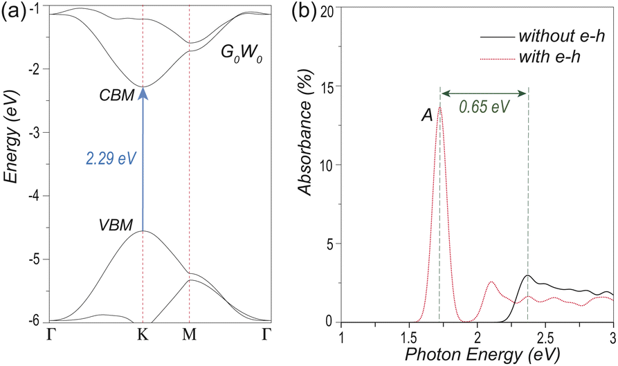 | ||
| Fig. 3 (a) The band structure of BNcG, as obtained from G0W0 calculations. The vertical dotted lines represent the high symmetric points. A direct band gap of 2.29 eV at the K point is depicted by the arrow. (b) Optical absorption spectra of BNcG as a function of in-plane photon energy, as obtained by considering the e–h interaction (the red dotted line) and without e–h interaction (black solid line). The first singlet bright excitonic peak is marked as A. The exciton binding energy of 0.65 eV is depicted by a double-headed arrow. | ||
To incorporate excitonic interaction, we further solve BSE using the following equation:41
 | (3) |
 | (4) |
In the GW level (without e–h interaction) the first peak of the absorption spectra appears at 2.37 eV which shows a good agreement with the calculated GW band gap. However, within the GW + BSE (with e–h interaction) level, the absorption peak (marked by A) corresponding to the first bright exciton appears at 1.72 eV which can be considered the optical gap. The inclusion of the excitonic many-body effect through the BSE corrects the GW optical gap by 0.57 eV (2.29–1.72 eV). The first two bright exciton peaks, as can be seen in Fig. 3(b), arise from doubly degenerate excitons. In between these two bright excitons, there exist two doubly degenerate dark excitons that do not contribute towards the absorption spectra. By subtracting the energy of the first bright exciton peak (A) from the energy of the first absorption peak obtained without considering e-h interaction, we estimate the excitonic binding energy to be 0.65 eV, as depicted in Fig. 3(b). Thus the GW + BSE absorption spectrum contains both the information of QP gap correction over the GW level theory and the formation of bound excitons which redshifts the GW + BSE absorption spectra as compared to the GW absorption spectra.
Among the two degenerate excitonic states that give rise to peak A, one localizes in K and the other localizes in the K′ valley. This degeneracy can be broken through the irradiation of circularly polarized light of different chiralities.28,42 To check the robustness of such an optical selection rule for exciton formation, in Fig. 4(a), we plot the k-resolved envelope function  (i denotes the degeneracy) for the first bright exciton (peak A) over the hexagonal Brillouin zone. It shows an extremely small (3.8%) intervalley coupling between K and K′ valleys. To confirm whether this small inter-valley coupling can cause valley depolarization or not, we further calculate the excitonic oscillator strength upon irradiation of left- and right-handed circularly polarized light as follows:22,43,44
 | (5) |
![[v with combining circumflex]](https://www.rsc.org/images/entities/char_0076_0302.gif) |ck〉 denotes the optical matrix element, that couples with left- and right-handed circularly polarized light, σ± with polarization vector P at opposite valleys. We plot the oscillator strength for left-(σ+) and right-handed (σ−) circularly polarized light in the first BZ as in Fig. 4(b) and (c) for the first bright exciton (peak A). As can be seen, the σ+ and σ− light selectively excites the K and K′ valleys. This clearly indicates selective excitation of only one valley with a certain helicity of circularly polarized light. Therefore, the absence of intervalley scattering along with high Berry curvature results in efficient valley polarization and the circular dichroism Hall effect in the BNcG system in the presence of the in-plane electric field.
|ck〉 denotes the optical matrix element, that couples with left- and right-handed circularly polarized light, σ± with polarization vector P at opposite valleys. We plot the oscillator strength for left-(σ+) and right-handed (σ−) circularly polarized light in the first BZ as in Fig. 4(b) and (c) for the first bright exciton (peak A). As can be seen, the σ+ and σ− light selectively excites the K and K′ valleys. This clearly indicates selective excitation of only one valley with a certain helicity of circularly polarized light. Therefore, the absence of intervalley scattering along with high Berry curvature results in efficient valley polarization and the circular dichroism Hall effect in the BNcG system in the presence of the in-plane electric field.
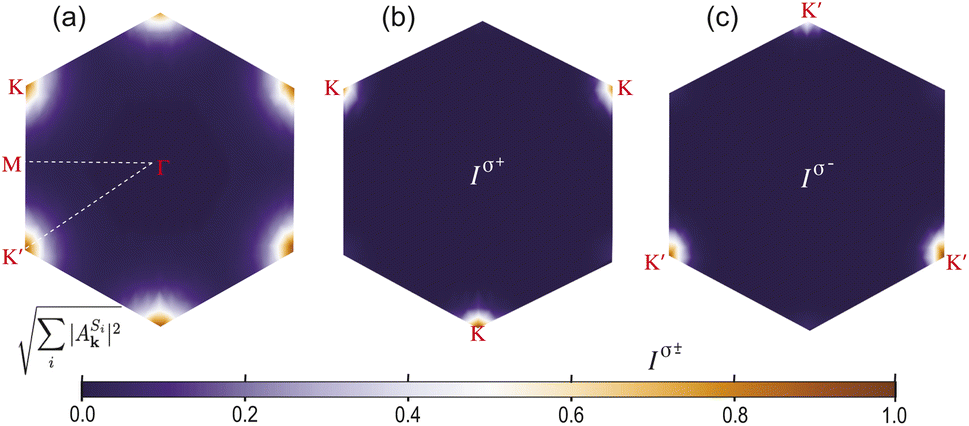 | ||
| Fig. 4 (a) The contour plot of the square root of the sum of the squared excitonic envelope function of the singlet bright exciton (peak A) of BNcG. The oscillator strengths of excitons in the presence of (b) left- and (c) right-handed circularly polarized light show selective excitations at K and K′ valleys, respectively. The colour bar depicts the normalized values of the envelope function and the oscillator strength. | ||
4 Conclusion
In conclusion, we propose a 2D honeycomb superlattice of graphene with periodic incorporation of B and N clusters with overall BC6N stoichiometry. The cohesive energy calculation along with the AIMD simulations proves the stability of this system even at room temperature. The presence of B and N clusters breaks the spatial inversion symmetry, however, preserving the time-reversal symmetry with a semiconducting gap at K and K′ valleys. Owing to this, the system exhibits a very high Berry curvature of 125.9 bohr2 at opposite valleys, which is considerably higher than that of other reported 2D materials. Explicit consideration of excitonic quasiparticles along with their scattering possibilities within the GW and many-body BSE formalism reveals an optical gap of 1.72 eV and a strong excitonic binding energy of 0.65 eV. Negligible intervalley scattering between the opposite valleys, as indicated by the envelope function calculation, ensures the robustness of the optical selection rule for valley selective optical excitations. This has been further established by explicit oscillator strength estimations in the presence of left- and right-handed circularly polarized light. Such efficient valley polarization can be exploited for circular dichroism valley Hall effect and excitonic qubit applications in advanced information processing.Data availability
The calculations have been carried out using the QUANTUM ESPRESSO package31 (https://www.quantum-espresso.org), Wannier90 code34 (https://wannier.org) and BerkeleyGW package35 (https://berkeleygw.org).Author contributions
SA defined the project. SB and SA performed all the computational calculations. SB, SA and SD analyzed the results and written, reviewed & edited the manuscript.Conflicts of interest
There are no conflicts to declare.Acknowledgements
SB, SA, and SD thank IISER Tirupati for Intramural Funding and the Science and Engineering Research Board, Dept. of Science and Technology, Govt. of India for the research grant (CRG/2021/001731). The authors acknowledge the National Supercomputing Mission (NSM) for providing computing resources of ‘PARAM Brahma’ at IISER Pune, which is implemented by C-DAC and supported by the Ministry of Electronics and Information Technology (MeitY) and DST, Govt. of India.Notes and references
- A. Rycerz, J. Tworzydło and C. Beenakker, Nat. Phys., 2007, 3, 172–175 Search PubMed
.
- K. F. Mak, D. Xiao and J. Shan, Nat. Photonics, 2018, 12, 451–460 CrossRef
- K. F. Mak, K. L. McGill, J. Park and P. L. McEuen, Science, 2014, 344, 1489–1492 CrossRef PubMed
- G. Pacchioni, Nat. Rev. Phys., 2020, 5, 480 Search PubMed
- S. A. Vitale, D. Nezich, J. O. Varghese, P. Kim, N. Gedik, P. Jarillo-Herrero, D. Xiao and M. Rothschild, Small, 2018, 14, 1801483 CrossRef PubMed
- H. Zeng, J. Dai, W. Yao, D. Xiao and X. Cui, Nat. Nanotechnol., 2012, 7, 490–493 CrossRef
- Z. Ye, D. Sun and T. F. Heinz, Nat. Phys., 2017, 13, 26–29 Search PubMed
- K. F. Mak, K. He, J. Shan and T. F. Heinz, Nat. Nanotechnol., 2012, 7, 494–498 CrossRef
- T. Cao, G. Wang, W. Han, H. Ye, C. Zhu, J. Shi, Q. Niu, P. Tan, E. Wang and B. Liu,
et al.
, Nat. Commun., 2012, 3, 887 CrossRef
- J. Qi, X. Li, Q. Niu and J. Feng, Phys. Rev. B, 2015, 92, 121403 CrossRef
- W. Xun, C. Wu, H. Sun, W. Zhang, Y.-Z. Wu and P. Li, Nano Lett., 2024, 24, 3541–3547 CrossRef PubMed
- P. Li, B. Liu, S. Chen, W.-X. Zhang and Z.-X. Guo, Chin. Phys. B, 2024, 33, 017505 CrossRef
- Q. Wang, S. Ge, X. Li, J. Qiu, Y. Ji, J. Feng and D. Sun, ACS Nano, 2013, 7, 11087–11093 CrossRef PubMed
- P. Li, C. Wu, C. Peng, M. Yang and W. Xun, Phys. Rev. B, 2023, 108, 195424 CrossRef
- P. Li, X. Yang, Q.-S. Jiang, Y.-Z. Wu and W. Xun, Phys. Rev. Mater., 2023, 7, 064002 CrossRef
- A. C. Neto, F. Guinea, N. M. Peres, K. S. Novoselov and A. K. Geim, Rev. Mod. Phys., 2009, 81, 109 CrossRef
- A. K. Geim and K. S. Novoselov, Nat. Mater., 2007, 6, 183–191 CrossRef CAS
- D. Gunlycke and C. T. White, Phys. Rev. Lett., 2011, 106, 136806 CrossRef CAS
- Z.-Y. Chen and R. Qin, Opt. Express, 2019, 27, 3761–3770 CrossRef CAS
- Y. Zhou and F. Liu, Nano Lett., 2020, 21, 230–235 CrossRef
- D. Xiao, W. Yao and Q. Niu, Phys. Rev. Lett., 2007, 99, 236809 CrossRef PubMed
- F. Zhang, C. S. Ong, J. W. Ruan, M. Wu, X. Q. Shi, Z. K. Tang and S. G. Louie, Phys. Rev. Lett., 2022, 128, 047402 CrossRef CAS PubMed
- Z. Song, Z. Li, H. Wang, X. Bai, W. Wang, H. Du, S. Liu, C. Wang, J. Han and Y. Yang,
et al.
, Nano Lett., 2017, 17, 2079–2087 CrossRef CAS PubMed
- C. Elias, P. Valvin, T. Pelini, A. Summerfield, C. Mellor, T. Cheng, L. Eaves, C. Foxon, P. Beton and S. Novikov,
et al.
, Nat. Commun., 2019, 10, 2639 CrossRef CAS
- S. Adhikary, S. Mohakud and S. Dutta, Phys. Rev. B, 2023, 108, 195429 CrossRef CAS
- L. Ci, L. Song, C. Jin, D. Jariwala, D. Wu, Y. Li, A. Srivastava, Z. Wang, K. Storr and L. Balicas,
et al.
, Nat. Mater., 2010, 9, 430–435 CrossRef CAS
- X. Liu, X. Ma, H. Gao, X. Zhang, H. Ai, W. Li and M. Zhao, Nanoscale, 2018, 10, 13179–13186 RSC
- S. Adhikary and S. Dutta, J. Phys.: Condens. Matter, 2023, 36, 125304 CrossRef
- K. Matsui, S. Oda, K. Yoshiura, K. Nakajima, N. Yasuda and T. Hatakeyama, J. Am. Chem. Soc., 2018, 140, 1195–1198 CrossRef CAS
- J. P. Perdew, K. Burke and M. Ernzerhof, Phys. Rev. Lett., 1996, 77, 3865 CrossRef CAS
- P. Giannozzi, S. Baroni, N. Bonini, M. Calandra, R. Car, C. Cavazzoni, D. Ceresoli, G. L. Chiarotti, M. Cococcioni and I. Dabo,
et al.
, J. Phys.: Condens. Matter, 2009, 21, 395502 CrossRef PubMed
- M. J. van Setten, M. Giantomassi, E. Bousquet, M. J. Verstraete, D. R. Hamann, X. Gonze and G.-M. Rignanese, Comput. Phys. Commun., 2018, 226, 39–54 CrossRef CAS
- H. J. Monkhorst and J. D. Pack, Phys. Rev. B, 1976, 13, 5188 CrossRef
- A. A. Mostofi, J. R. Yates, Y.-S. Lee, I. Souza, D. Vanderbilt and N. Marzari, Comput. Phys. Commun., 2008, 178, 685–699 CrossRef CAS
- J. Deslippe, G. Samsonidze, D. A. Strubbe, M. Jain, M. L. Cohen and S. G. Louie, Comput. Phys. Commun., 2012, 183, 1269–1289 CrossRef CAS
- L. Qu, Y. Liu, J.-B. Baek and L. Dai, ACS Nano, 2010, 4, 1321–1326 CrossRef CAS
- D. Usachov, O. Vilkov, A. Gruneis, D. Haberer, A. Fedorov, V. K. Adamchuk, A. B. Preobrajenski, P. Dudin, A. Barinov, M. Oehzelt, C. Laubschat and D. Vyalikh, Nano Lett., 2011, 11, 5401–5407 CrossRef CAS
- A. Lherbier, X. Blase, Y.-M. Niquet, F. Triozon and S. Roche, Phys. Rev. Lett., 2008, 101, 036808 CrossRef
- L. Lin, J. Li, Q. Yuan, Q. Li, J. Zhang, L. Sun, D. Rui, Z. Chen, K. Jia and M. Wang,
et al.
, Sci. Adv., 2019, 5, eaaw8337 CrossRef CAS PubMed
- M. S. Hybertsen and S. G. Louie, Phys. Rev. B: Condens. Matter Mater. Phys., 1986, 34, 5390 CrossRef CAS PubMed
- M. Rohlfing and S. G. Louie, Phys. Rev. B: Condens. Matter Mater. Phys., 2000, 62, 4927 CrossRef CAS
- D. Y. Qiu, F. H. Da Jornada and S. G. Louie, Phys. Rev. Lett., 2013, 111, 216805 CrossRef
- D. Xiao, G.-B. Liu, W. Feng, X. Xu and W. Yao, Phys. Rev. Lett., 2012, 108, 196802 CrossRef PubMed
- P. T. Mahon, R. A. Muniz and J. Sipe, Phys. Rev. B, 2019, 100, 075203 CrossRef CAS
Footnotes |
| † Electronic supplementary information (ESI) available. See DOI: https://doi.org/10.1039/d4na00759j |
| ‡ Present address: Department of Nanotechnology for Sustainable Energy, School of Science and Technology, Kwansei Gakuin University, 1-Gakuen Uegahara, Sanda 669-1330, Hyogo, Japan. |
| This journal is © The Royal Society of Chemistry 2025 |