
 Open Access Article
 This Open Access Article is licensed under a Creative Commons Attribution-Non Commercial 3.0 Unported Licence
Electromigration-driven linear actuator operations of Co nanorods inside and outside multi-walled carbon nanotubes with stroke of tens of nanometers†
Shogo
Matsuyama
a and
Hideo
Kohno
 *bc
*bc
aDepartment of Engineering, Graduate School of Engineering, Kochi University of Technology, Kami, Kochi 782-8502, Japan
bSchool of Engineering Science, Kochi University of Technology, Kami, Kochi 782-8502, Japan. E-mail: kohno.hideo@kochi-tech.ac.jp; Fax: +81 887-57-2520; Tel: +81 887-57-2506
cCenter for Nanotechnology, Kochi University of Technology, Kami, Kochi 782-8502, Japan
First published on 3rd December 2024
Abstract
Solid Co nanorod fillers were pushed out of multi-walled carbon nanotubes via electromigration and their behaviors were observed in situ by transmission electron microscopy. When a solid Co nanorod was pushed out, the portion outside the nanotube increased in diameter. The behavior of the plastic deformation depended on the crystal orientation of the Co nanorod filler. When the direction of the electron flow was reversed, the Co nanorod was pulled into the host nanotube. In one trial, the Co nanorod was split into two portions inside the nanotube near one of the electrodes.
1 Introduction
For the development of nanoscale mechanical machines1,2 and nano-mechanics,3,4 methods for the functional manipulation of nano-objects and the precise control of their motion are necessary. Various physical phenomena have been utilized to manipulate nano-objects, such as electric forces,5,6 bond length changes,7 thermal volume changes,8,9 thermomigration,10–13 the capillary effect,11,14–16 and electromigration.10,17–21 Although thermal volume changes are reversible, they are unsuitable for long-stroke manipulation. It is very difficult to use the capillary effect for reversible motion. For reversible thermomigration, it is necessary to precisely control the temperature distribution. Electric forces can be used for reversible motion, but well-aligned electrodes are required to control the motion. Electromigration has potential for the controlled reversible motion of nano-objects, whose direction of motion can be simply changed by switching the direction of electric current.11,18,22–25 The motion of a metallic nano-object is along the direction of electron flow (i.e., opposite to the direction of the electric current) because the electrons impart momentum to the metal atoms.26–30 Ions are subjected to the electric field and electron wind forces.In our previous study,31 we developed a method for determining the electron wind force and the sliding friction force on Co nanorod fillers32–35 inside multi-walled carbon nanotubes (MWCNTs).36 The results of the previous study enable us to control the motion of a Co nanorod filler in a MWCNT. In the present study, we apply the method of controlled operations of Co fillers developed in our previous study31 to nano-engineering. We perform long-stroke continuous linear actuator operations using solid Co nanorod fillers inside and outside MWCNTs. We conduct in situ transmission electron microscopy observations of the operations and investigate the plastic deformation of the Co nanorod fillers during the operations. In our previous studies,31,37 operations of Co nanorod fillers were limited inside MWCNTs. In this study, operations of Co nanorod fillers are not limited inside host MWCNTs. Co nanorod fillers were pushed out of the host MWCNTs and deformation of the Co nanorod fillers outside the MWCNTs were investigated.
2 Experimental
To fabricate MWCNTs with Co nanorod fillers, we followed the procedure used in our previous study.31 Briefly, a polycrystalline alumina substrate with a 30 nm-thick Co deposition layer on its surface was sealed in an evacuated silica glass tube with 3 mg of a mixture of graphite, hexadecanoic acid, and saccharin at a weight ratio of 664![[thin space (1/6-em)]](https://www.rsc.org/images/entities/char_2009.gif) :86:1. The sample was heated at 1100 °C for 20 min for growth. The grown MWCNTs with Co nanorod fillers were mounted on an Au wire that served as the ground electrode for TEM (JEOL JEM-ARM200F) observations at an accelerating voltage of 200 kV. Results of TEM-based analysis of a formed nanostructure is provided in ESI.† A W needle was used as the bias electrode. TEM images were recorded using a camera (Gatan Rio16) with a resolution of 1024 × 1024 pixels at 25 frames per second. A source measure unit (Yokogawa GS610) was used to apply and measure electric current.
:86:1. The sample was heated at 1100 °C for 20 min for growth. The grown MWCNTs with Co nanorod fillers were mounted on an Au wire that served as the ground electrode for TEM (JEOL JEM-ARM200F) observations at an accelerating voltage of 200 kV. Results of TEM-based analysis of a formed nanostructure is provided in ESI.† A W needle was used as the bias electrode. TEM images were recorded using a camera (Gatan Rio16) with a resolution of 1024 × 1024 pixels at 25 frames per second. A source measure unit (Yokogawa GS610) was used to apply and measure electric current.
A schematic illustration of the experimental setup for the electromigration experiments is shown in Fig. 1(a). The W needle was placed at the middle of a Co nanorod filler to apply an electric current. The portion of the Co nanorod filler between its left end and the electric contact with the W needle was forced to move along the direction of electron flow. No electromigration force was applied to the portion of the Co nanorod filler between its right end and the electric contact because the electric current did not flow through the right portion. The direction of the electromigration force can be changed by changing the polarity.
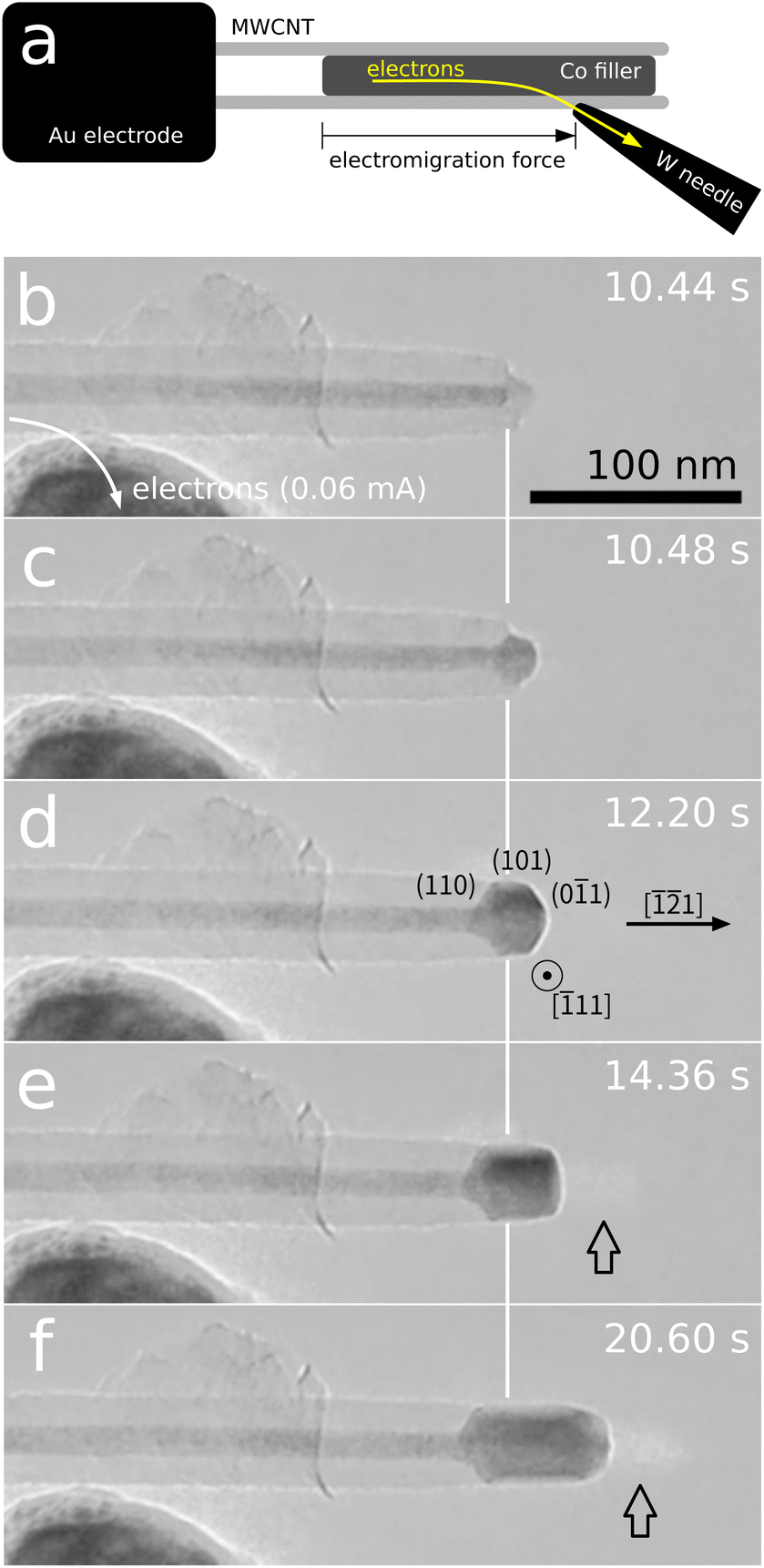 | ||
| Fig. 1 (a) Schematic illustration of experimental setup. (b–f) In situ TEM images of electromigration manipulation of a Co nanorod filler. The Co filler was pushed out of the MWCNT to the right by the electromigration force. The vertical white lines indicate the initial position of the right end of the Co filler. The arrows indicate bright images of the Co nanorod formed with a Bragg-reflected wave (ESI movie† SM1 available). | ||
3 Results and discussion
An example of the experimental results is shown in Fig. 1(b–f) and ESI movie† SM1. The outer diameter of the MWCNT was 43 and 35 nm in the middle and at the tip, respectively. The Co nanorod filler was 14 nm in diameter. Before an electric current was applied, the position of the right end of the Co filler was almost the same as that of the right end of the MWCNT and the MWCNT's right end was open, as shown in Fig. 1(b). When an electric current of 0.060 mA was applied, the Co filler moved to the right and part of it was pushed out of the MWCNT, as shown in Fig. 1(c).For the estimation of the current density in the Co filler, we used the reported values of resistivity, 9.8 × 10⁻⁶ and 6.24 × 10⁻⁸ [Ohm m] for graphite (perpendicular to the c-axis) and Co, respectively. The MWCNT and the Co nanorod filler formed a simple parallel current divider, therefore the current was divided into two according to the values of resistivity and the cross-section areas. The current density in the Co nanorod filler was estimated to be ca. 0.37 ± 0.11 μA nm−2. This high value of the current density would have been necessary because the Co nanorod filler was crystalline and the sliding was hampered by the contacting MWCNT.
During the application of the electric current, the portion outside the MWCNT became larger and eventually the filler diameter increased to 35 nm, which is the outer diameter of the MWCNT at its tip, as shown in Fig. 1(d). With further application of the electric current, the thicker portion of the filler outside the MWCNT became longer along the axis of the MWCNT while the diameter remained equal to the outer diameter of the MWCNT [Fig. 1(e) and (f)]. The portion outside the MWCNT was faceted, as shown in Fig. 1(d), and showed a bright image of the Co nanorod formed with a Bragg-reflected wave,38 as indicated by the arrows in Fig. 1(e) and (f). This indicates that the Co nanorod filler was solid during the process. The facets of the outer portion of the Co nanorod in Fig. 1(c) were indexed based on shape. The crystal orientation of the Co nanorod along the MWCNT's axis was [![[1 with combining macron]](https://www.rsc.org/images/entities/char_0031_0304.gif)
![[2 with combining macron]](https://www.rsc.org/images/entities/char_0032_0304.gif) 1] and the viewing direction was [11]. The orientations of the sidewalls of the Co filler outside the MWCNT were mainly {011}. These low-index surfaces were parallel to the MWCNT's axis, and thus it is likely that the increase in diameter stopped. Because the observation was in only one direction, complete information of the three-dimensional shape of the Co nanorod was not obtained.
1] and the viewing direction was [11]. The orientations of the sidewalls of the Co filler outside the MWCNT were mainly {011}. These low-index surfaces were parallel to the MWCNT's axis, and thus it is likely that the increase in diameter stopped. Because the observation was in only one direction, complete information of the three-dimensional shape of the Co nanorod was not obtained.
At the initial stage of the process, the right tip of the MWCNT was eroded by the Co filler [Fig. 1(c–e)]. This erosion eventually stopped [Fig. 1(f)]. It is likely that an increase in temperature due to Joule heating caused this erosion and that the eroded portion dissolved into the Co filler at high temperature. It is likely that the erosion stopped because the concentration of C in the Co nanorod reached the solid solubility limit. The temperature was below the melting point of Co (1768 K), as evidenced by the Co filler being solid during the process. About the estimate of the temperature during electromigration motions, see our previous report.31 We speculate the temperature was below 1000 °C. For more precise estimation of temperature during the process, many nanoparticles of various materials with different melting temperatures deposited on the surface of MWCNTs would be useful; however, those many nanoparticles would prevent in situ TEM observations.
Fig. 2 and ESI movie† SM2 show another example of a Co nanorod filler being pushed out using the same experimental setup. The MWCNT and the Co nanorod filler were 27 and 12 nm in diameter, respectively. The electric current was increased gradually, as shown in Fig. 2(f). As the electric current was increased, the Co filler was pushed out of the MWCNT [Fig. 2(b)]. When the electric current was 0.040 mA, the diameter of the portion of the Co filler outside the MWCNT became larger than that of the MWCNT, as shown in Fig. 2(c). A further increase in the electric current resulted in further growth of the portion of Co outside the MWCNT, as shown in Fig. 2(d) and (e). Fig. 2(d) and (e) also show the formation of a new electric contact between the Co filler outside the MWCNT and the W needle.
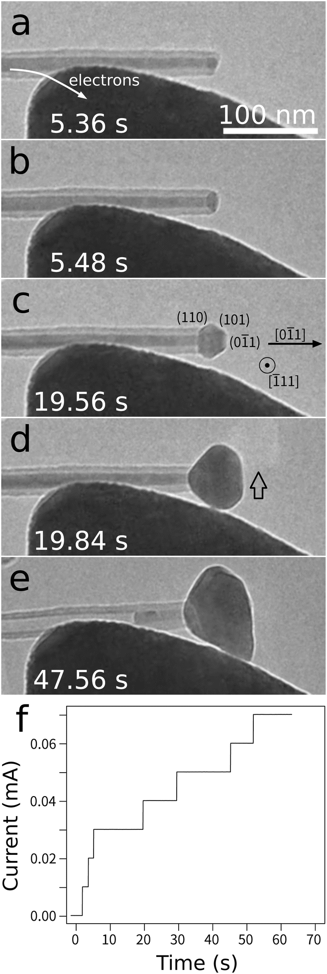 | ||
| Fig. 2 (a–e) In situ TEM images of electromigration manipulation of a Co nanorod filler. The Co filler was pushed out of the MWCNT to the right by the electromigration force. The arrow in (d) indicates a bright image of the portion of the Co nanorod outside the MWCNT formed with a Bragg-reflected wave. (f) Plot of current as a function of time (ESI movie† SM2 available). | ||
As shown in Fig. 2(c), the portion outside the MWCNT was clearly faceted. The facets were indexed as {011} based on shape. The direction along the MWCNT's axis was [01]and the viewing direction was [11]. The crystal orientation of the Co filler in Fig. 2(c) along the MWCNT's axis is rotated by 30° (or 90°) with respect to that of the first example show in Fig. 1(d). The portion of the filler outside the MWCNT showed a bright image of the Co nanorod formed with a Bragg-reflected wave, as indicated by the arrow in Fig. 2(d). The faceting and the bright image of the Co nanorod formed with a Bragg-reflected wave indicate that the Co filler was solid during the process.
In the first example (Fig. 1), the portion of the Co filler outside the MWCNT was as thick as the MWCNT, whereas in the second example (Fig. 2), the portion outside the MWCNT grew thicker than the host MWCNT. We speculate that this difference was caused by the difference in crystal orientation between the two Co crystals. In the first example, the sidewalls of the portion outside the MWCNT consisted of low-index facets that were parallel to the axis of the MWCNT, whereas in the second example, the sidewalls of the portion outside the MWCNT did not consist of parallel, low-index facets. We confirmed that the crystal orientations of two portions of a Co nanorod inside and outside its host MWCNT were the same as shown in ESI.† It is likely that the initial crystal orientation of a Co nanorod filler inside the host MWCNT determines its behavior when it is pushed out of the MWCNT during electromigration motion. When the sidewalls of a Co nanorod consist of parallel, low-index facets, the nanorod would maintain its shape when it is pushed out of the host MWCNT because the low-index facets have low surface energies. In the other case, a Co nanorod would change its shape largely forming low-index facets when it is pushed out of the host MWCNT.
We also performed a push-out/pull-in operation. Fig. 3 and ESI movie† SM3 show the in situ observation of the push-out/pull-in operation. A flattened MWCNT mounted on a W needle was used as the bias electrode. The MWCNT electrode allowed clear observation of the operation. The MWCNT and the Co filler were about 46 and 13 nm in diameter, respectively. Initially, the Co nanorod filler was located about 140 nm inside from the open end of the MWCNT [Fig. 3(a)]. When an electric current was applied, the Co filler was pushed to the right [Fig. 3(b)]. Then, the right end of the Co filler pushed out of the MWCNT, increasing in diameter until it matched that of the MWCNT [Fig. 3(c)]. The portion outside the MWCNT became longer, reaching about 110 nm, during the application of the electric current [Fig. 3(d) and (e)]. This behavior is similar to that of the first example shown in Fig. 1. Therefore, we speculate that the crystal orientation of the Co fillers were similar. When the direction of the electron flow reversed, the Co filler was pulled in [Fig. 3(f)] and the portion outside the MWCNT became shorter, reaching about 80 nm. The Co filler split into two fragments. The left fragment inside the MWCNT was pulled to the left along the electron flow, whereas the right fragment was stuck outside [Fig. 3(g)]. During the process, the Co nanorod filler showed a bright image formed with a Bragg-reflected wave, which indicates that it was solid. We note that Co fillers were also solid during electromigration motions inside MWCNTs in our previous studies.31,37
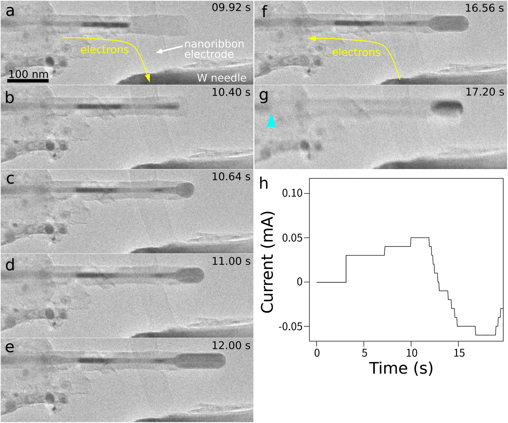 | ||
| Fig. 3 (a–g) In situ TEM images of electromigration manipulation of a Co nanorod filler. The Co filler was first pushed out of the MWCNT and then pulled into the MWCNT when the direction of electron flow was reversed. The filler split into two portions at the shoulder. The blue arrow head in (g) indicates the position of the right end of the left portion. (h) Plot of current as a function of time. The direction of electron flow was reversed at around 13.0 s (ESI movie† SM3 available). | ||
The results of a second trial of the push-out/pull-in operation are shown in Fig. 4 and ESI movie† SM4. The MWCNT and the Co filler were about 28 and 13 nm in diameter, respectively. In this case, the Co filler became thicker than the diameter of the host MWCNT when it was pushed out, similar to the second example shown in Fig. 2. It is likely that the low-index facets were not parallel to the axis of the MWCNT, as was the case for the example shown in Fig. 2. When the direction of the electron flow was reversed, the Co filler split into two fragments, with the left portion inside the MWCNT pulled to the left along the electron flow and the right portion left outside without changing its volume. The Co filler showed clear facets and a bright image formed with a Bragg-reflected wave, which indicates that it was solid during the process. As shown by this example, the pull-in operation is not straightforward and it is likely that the pull-in behavior strongly depends on the crystal orientation of the Co filler.
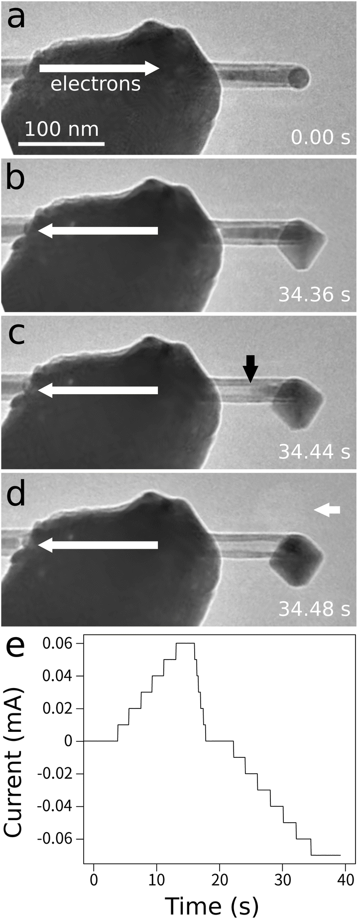 | ||
| Fig. 4 (a–d) In situ TEM images of electromigration manipulation of a Co nanorod filler. The Co filler was pushed out of the MWCNT. The outside portion grew thicker than the diameter of the MWCNT. Then, the direction of electron flow was reversed. The Co filler split into two fragments, with the left fragment inside the MWCNT pulled to the left and the right fragment left outside the MWCNT, unmoved and unchanged. The black arrow in (c) indicates the location of the fragmentation. The white arrow in (d) indicates a bright image of the Co fragment outside the MWCNT formed with a Bragg-reflected wave. (e) Plot of current as a function of time. The direction of electron flow was reversed at around 22.2 s (ESI movie† SM4 available). | ||
4 Conclusions
In conclusion, continuous push-out and pull-in operations of solid Co nanorod fillers inside and outside MWCNTs were realized using electromigration. In situ TEM observations revealed plastic deformation of the Co nanorod fillers during these operations. The portion pushed out of the host MWCNT did not maintain its initial nanorod shape. Its diameter became as large as or larger than that of the host MWCNT. In some cases, the increase in diameter was limited to that of the host MWCNT. It is very likely that the crystal orientation of the Co nanorod filler affects the plastic deformation behavior. The push-out operation was easy to perform, whereas the pull-in operation did not always succeed. It appears that the pull-in operation also depends on the crystal orientation of the Co nanorod filler. This study demonstrated that Co fillers in MWCNTs can perform the basic operations of an indenter, pipette, and linear actuator. The controlled linear operations of Co fillers in MWCNTs will add unique functionalities to MEMS systems and facilitate materials science experiments. We also expect the continuous push-out and pull-in operations of solid Co nanorod fillers inside and outside MWCNTs would be useful for fabricating nanoarchitectured functional materials39 by using the operations to connect CNTs. We expect the universality of the observed phenomenon beyond the MWCNTs.Data availability
The data supporting this article have been included as part of the ESI.†Conflicts of interest
There are no conflicts to declare.References
- B. Xu, P. Zhang, J. Zhu, Z. Liu, A. Eichler, X.-Q. Zheng, J. Lee, A. Dash, S. More and S. Wu, et al. , ACS Nano, 2022, 16, 15545–15585 CAS.
- K. Ariga, T. Mori and J. P. Hill, Adv. Mater., 2012, 24, 158–176 CrossRef CAS.
- D. Srivastava, C. Wei and K. Cho, Appl. Mech. Rev., 2003, 56, 215–230 CrossRef.
- M. Mora, A. Stannard and S. Garcia-Manyes, Chem. Soc. Rev., 2020, 49, 6816–6832 RSC.
- L. Dong, B. J. Nelson, T. Fukuda and F. Arai, IEEE Trans. Autom. Sci. Eng., 2006, 3, 228–235 Search PubMed.
- A. Fennimore, T. Yuzvinsky, W.-Q. Han, M. Fuhrer, J. Cumings and A. Zettl, Nature, 2003, 424, 408–410 CrossRef CAS PubMed.
- R. H. Baughman, C. Cui, A. A. Zakhidov, Z. Iqbal, J. N. Barisci, G. M. Spinks, G. G. Wallace, A. Mazzoldi, D. De Rossi and A. G. Rinzler, et al. , Science, 1999, 284, 1340–1344 CrossRef CAS.
- Y. Gao and Y. Bando, Nature, 2002, 415, 599 CrossRef CAS PubMed.
- Y. Gao, Y. Bando, Z. Liu, D. Golberg and H. Nakanishi, Appl. Phys. Lett., 2003, 83, 2913–2915 CrossRef CAS.
- R. Zou, Z. Zhang, Q. Liu, K. Xu, A. Lu, J. Hu, Q. Li, Y. Bando and D. Golberg, Adv. Mater., 2013, 25, 2693–2699 CrossRef CAS.
- R. Bekarevich, M. Toyoda, S. Baba, T. Nakata and K. Hirahara, Nanoscale, 2016, 8, 7217–7223 RSC.
- M. Okada, D. Sasaki and H. Kohno, Microscopy, 2020, 69, 291–297 CrossRef CAS PubMed.
- D.-G. Xie, Z.-Y. Nie, S. Shinzato, Y.-Q. Yang, F.-X. Liu, S. Ogata, J. Li, E. Ma and Z.-W. Shan, Nat. Commun., 2019, 10, 4478 CrossRef PubMed.
- P. M. Ajayan and S. Ijima, Nature, 1993, 361, 333–334 CrossRef CAS.
- D. Schebarchov and S. Hendy, Nano Lett., 2008, 8, 2253–2257 CrossRef CAS PubMed.
- K. Jayaraman, K. Okamoto, S. J. Son, C. Luckett, A. H. Gopalani, S. B. Lee and D. S. English, J. Am. Chem. Soc., 2005, 127, 17385–17392 CrossRef CAS.
- C. Jin, K. Suenaga and S. Iijima, Nat. Nanotechnol., 2008, 3, 17–21 CrossRef CAS PubMed.
- G. Melinte, S. Moldovan, C. Hirlimann, X. Liu, S. Bégin-Colin, D. Bégin, F. Banhart, C. Pham-Huu and O. Ersen, Nat. Commun., 2015, 6, 8071 CrossRef CAS.
- S. Sharma, M. S. Rosmi, Y. Yaakob, M. Z. M. Yusop, G. Kalita, M. Kitazawa and M. Tanemura, Carbon, 2018, 132, 165–171 CrossRef CAS.
- K. Ichigi, H. Kohno and J. Jpn, Appl. Phys., 2020, 59, 108001 CAS.
- L.-B. He, L. Shangguan, Y.-T. Gao, S. Yang, Y.-T. Ran, Z.-Y. Lu, J.-H. Zhu, B.-J. Wang and L.-T. Sun, ACS Appl. Nano Mater., 2023, 6, 7679–7685 CrossRef CAS.
- Y. Naitoh, M. Horikawa, H. Abe and T. Shimizu, Nanotechnology, 2006, 17, 5669 CrossRef CAS PubMed.
- C. Schirm, M. Matt, F. Pauly, J. C. Cuevas, P. Nielaba and E. Scheer, Nat. Nanotechnol., 2013, 8, 645–648 CrossRef CAS PubMed.
- T. Kozlova, M. Rudneva and H. W. Zandbergen, Nanotechnology, 2013, 24, 505708 CrossRef PubMed.
- J. Lombardo, S. Collienne, A. Petrillo, E. Fourneau, N. D. Nguyen and A. Silhanek, New J. Phys., 2019, 21, 113015 CrossRef CAS.
- J. R. Black, IEEE Trans. Electron Devices, 1969, 16, 338–347 CAS.
- R. Landauer and J. W. Woo, Phys. Rev. B, 1974, 10, 1266 CrossRef.
- P. S. Ho and T. Kwok, Rep. Prog. Phys., 1989, 52, 301 CrossRef CAS.
- R. De Orio, H. Ceric and S. Selberherr, Microelectron. Reliab., 2010, 50, 775–789 CrossRef CAS.
- K.-N. Tu, J. Appl. Phys., 2003, 94, 5451–5473 CrossRef CAS.
- K. Adachi, S. Matsuyama, Y. Sakai and H. Kohno, Nanoscale Adv., 2024, 6, 1480–1485 RSC.
- V. Blank, B. Kulnitskiy, I. Perezhogin, E. Polyakov and D. Batov, Acta Mater., 2010, 58, 1293–1298 CrossRef CAS.
- A. Leonhardt, S. Hampel, C. Mueller, I. Moench, R. Koseva, M. Ritschel, D. Elefant, K. Biedermann and B. Buechner, Chem. Vap. Depos., 2006, 12, 380–387 CrossRef CAS.
- A. S. Andreev, B. A. Kazakova, A. V. Ishchenko, A. G. Selyutin, O. B. Lapina, V. L. Kuznetsov and J.-B. d. de Lacaillerie, Carbon, 2017, 114, 39–49 CrossRef CAS.
- N. Singh and G. D. Aul, SN Appl. Sci., 2020, 2, 2026 CrossRef CAS.
- S. Iijima, Nature, 1991, 354, 56–58 CrossRef CAS.
- S. Matsuyama, K. Kumon and H. Kohno, Appl. Phys. Lett., 2024, 124, 243507 CrossRef CAS.
- A. Tonomura, T. Matsuda and J. Endo, Jpn. J. Appl. Phys., 1979, 18, 1373 CrossRef CAS.
- M. Aono and K. Ariga, Adv. Mater., 2016, 28, 989–992 CrossRef CAS.
Footnote |
| † Electronic supplementary information (ESI) available: Movie SM1-3. See DOI: https://doi.org/10.1039/d4na00766b |
| This journal is © The Royal Society of Chemistry 2025 |