
 Open Access Article
 This Open Access Article is licensed under a
 Creative Commons Attribution 3.0 Unported Licence
Stacking-dependent and electric field-driven electronic properties and band alignment transitions in γ-GeSe/Ga2SSe heterostructures: a first-principles study
Nguyen V.
Vinh
a,
D. V.
Lu
 b and
K. D.
Pham
*cd
b and
K. D.
Pham
*cd
aFaculty of Information Technology, Ho Chi Minh City University of Economics and Finance, Ho Chi Minh City, Vietnam. E-mail: vinhnv@uef.edu.vn
bFaculty of Physics, The University of Danang – University of Science and Education, Da Nang, 550000, Vietnam. E-mail: dvlu@ued.udn.vn
cInstitute of Research and Development, Duy Tan University, Da Nang 550000, Vietnam. E-mail: phamdinhkhang@duytan.edu.vn
dSchool of Engineering & Technology, Duy Tan University, Da Nang 550000, Vietnam
First published on 12th December 2024
Abstract
In this work, we present a comprehensive investigation into the electronic properties and contact behavior of γ-GeSe/Ga2SSe heterostructures using first-principles calculations. Two stacking configurations, γ-GeSe/SGa2Se and γ-GeSe/SeGa2S, are explored, both exhibiting semiconducting behavior with type-II and type-I band alignments, respectively. Notably, our results show that the band alignment transition in these heterostructures can occur spontaneously by simply altering the stacking configuration, eliminating the need for external factors. Additionally, the electronic properties of these heterostructures are highly tunable with an applied electric field, further enabling transitions between type-I and type-II alignments. Specifically, a positive electric field induces a transition from type-II to type-I alignment in the γ-GeSe/SGa2Se heterostructure, while a negative field drives the reverse transition in the γ-GeSe/SeGa2S heterostructure. Our findings underscore the potential of γ-GeSe/Ga2SSe heterostructures for diverse applications, where the tunability of electronic properties is crucial for optimizing device performance.
1 Introduction
Two-dimensional (2D) materials have garnered significant attention in recent years due to their exceptional electronic and optoelectronic properties, which arise from their atomic-scale thickness and unique crystal structures.1–3 Graphene,4 the first 2D material to be isolated and studied extensively, has served as a foundation for exploring the vast potential of this new class of materials. Following the discovery of graphene, a variety of other 2D materials have been identified, each with distinct properties that further expand the possibilities for advanced applications. Transition metal dichalcogenides (TMDs)5,6 exhibit tunable band gaps and strong light–matter interactions, making them suitable for optoelectronic devices and energy conversion applications. Similarly, hexagonal boron nitride (hBN) is valued for its insulating properties and chemical stability, often serving as a dielectric layer in 2D material-based devices.7,8 Despite the remarkable properties and potential applications of 2D materials, they also present several challenges and disadvantages that must be addressed to fully realize their potential in practical devices. For instance, the lacks in a band gap9 of graphene make it less suitable for applications that require a clear distinction between on and off states, such as digital transistors.10 In contrast, MoS2, a member of TMDs family, possess an intrinsic band gap,11 making it more suitable for semiconductor applications. However, the relatively low carrier mobility in MoS2 (ref. 12) compared to graphene limits its performance in high-speed electronics, where fast switching speeds and high conductivity are essential.Recently, numerous 2D materials have continuously been discovered and successfully synthesized in experiments. Among these, a newly discovered 2D material, namely γ-GeSe,13 has successfully fabricated using chemical vapor deposition (CVD) method. γ-GeSe has garnered significant interest due to its predicted Mexican-hat band structure, which offers unique electronic properties.14 Furthermore, the electronic properties and thermoelectric performance of γ-GeSe have been found to be highly sensitive to various external conditions such as strain engineering,15,16 layer thickness17 and doping.18,19 The versatility in the physical properties of γ-GeSe makes it promising candidate for a wide range of applications, such as thermoelectric13 and energy-related20,21 technologies. Similar to γ-GeSe, a new family of 2D materials known as Janus 2D structures has also been recently synthesized using the CVD method.22–24 These Janus materials are characterized by their asymmetrical structure, where different atomic species occupy each side of the layer. The successful synthesis of Janus 2D materials marks an exciting development in the field, offering new opportunities for designing multifunctional devices with tailored properties. Alongside with the experimental achievements, various 2D Janus structures based on 2D MX2 and 2D MX materials have also been computationally predicted. Among these, Ga2SSe Janus structures have garnered interest due to its extraordinary properties, such as high carrier mobility,25 adjustable electronic properties under strain,26,27 adsorption28 and making vertical heterostructures.29–31
Currently, the integration of different 2D materials into heterostructures32–36 has emerged as a transformative approach for enhancing and tailoring the performance of electronic and optoelectronic devices. By stacking layers of two or more 2D materials, the 2D heterostructures can be designed with engineered band alignments and unique interfacial properties that may absent in the individual layers. The van der Waals (vdW) heterostructures, characterized by weak vdW forces rather than covalent bonds, offer precise control over electronic interactions at the interfaces, enabling the design of multifunctional devices with designed properties.37–39 In recent years, the focus has increasingly shifted towards integrating 2D materials with tunable electronic properties to achieve high-performance devices with enhanced functionality. The integration between γ-GeSe or Janus Ga2SSe material with other 2D materials have been designed previously. For example, Huan et al.40 theoretically designed the integration of γ-GeSe and 2D h-BN/graphene/MoS2 material. They demonstrated that the γ-GeSe/h-BN heterostructure exhibits a type-I band alignment, while the γ-GeSe/MoS2 heterostructure exhibits a Z-scheme type. Cao et al.41 indicated that the integration between 2D metallic NbS2 and γ-GeSe induces an ohmic contact, while the Bi/γ-GeSe heterostructure exhibits a Schottky contact with ultra low contact barrier. Similarly, the integration between Ga2SSe and other 2D materials, such as ZnO,29 graphene,42 MoSSe43 and silicane44 has been designed and extensively studied. All these heterostructures have shown promising results in enhancing electronic and optical properties, further expanding the potential of 2D materials in next-generation devices. However, the integration between γ-GeSe and Janus Ga2SSe materials has not yet been explored or investigated. Herein, we have designed the γ-GeSe/Ga2SSe heterostructure and systematically investigated its electronic properties and contact characteristics. Additionally, we explored the influence of various stacking configurations, applied electric fields, and strain engineering on the heterostructure performance. These investigations provide valuable insights into the tunability of the electronic properties and potential applications of the γ-GeSe/Ga2SSe heterostructure in advanced electronic and optoelectronic devices.
2 Computational methods
All computations were carried out using density functional theory (DFT) as implemented in the Quantum Espresso.45 The exchange–correlation interactions were described using the generalized gradient approximation (GGA)46 with the Perdew–Burke–Ernzerhof (PBE) functional.46 The projector augmented wave (PAW)47 pseudopotential was utilized for describing the electron-ion effect. To accurately describe the weak interactions between layers in the heterostructure, we employed the Grimme DFT-D3 correction method.48 A plane-wave basis set with an energy cutoff of 510 eV was used for all calculations to ensure reliable convergence. To prevent the interactions between periodic images of the structure, a vacuum spacing of 30 Å was introduced along the z direction of materials. The Brillouin zone was sampled using a 9 × 9 × 1 Monkhorst–Pack k-point grid. Structural relaxations were performed until the forces on each atom were less than 0.01 eV Å−1, and the total energy was converged to within 10−6 eV. The dipole corrections were also applied in all calculations. The ab initio molecular dynamics (AIMD) simulations were conducted using a canonical ensemble (NVT) along with the Nose–Hoover thermostat.49 Additionally, a 3 × 3 × 1 supercell as employed to provide adequate sampling of the system, and the simulations were performed over a duration of 5 ps with a 1 fs time step at room temperature (300 K).3 Results and discussion
We begin by examining the atomic structures and electronic characteristics of the γ-GeSe and Janus Ga2SSe monolayers. Both materials exhibit a hexagonal lattice structure. The Janus Ga2SSe monolayer is classified under the point group C3v (P3m1), while the γ-GeSe monolayer is categorized under the point group C6v (6mm). Each unit cell of the Janus Ga2SSe monolayer contains a total of four atoms, comprising two gallium (Ga) atoms, one sulfur (S) atom, and one selenium (Se) atom. An unit cell of the γ-GeSe monolayer consists of two germanium (Ge) atoms and two Se atoms. Both Ga2SSe and γ-GeSe monolayers are classified as indirect semiconductors, with the conduction band minimum (CBM) located at the Γ point and the valence band maximum (VBM) found along the K–Γ path. The obtained band gap of γ-GeSe is 0.57 eV predicted by PBE method and 1.0 eV given by HSE method. While the Ga2SSe monolayer shows a larger band gap of 2.07 eV for PBE and 2.98 eV for HSE method. It is well established that the HSE method offers a more accurate estimation of the band gap compared to PBE. However, PBE remains a reasonable approach for investigating trends and qualitative behavior in both the γ-GeSe and Ge2SSe monolayers as well as their corresponding heterostructures. This is because the consistency between the HSE-calculated results for those monolayers and the trends observed using PBE lends confidence to the reliability of PBE for capturing the electronic properties in such materials. Furthermore, the stability of both monolayers is confirmed by the absence of imaginary frequencies in their phonon spectra at the Γ point, as illustrated in Fig. 1(c) and (f). The obtained lattice constants of γ-GeSe and Ga2SSe monolayers are 3.74 and 3.72 Å, respectively, as illustrated in Table 1. These values are in good agreement with the previous reports,25,50 confirming the reliability and accuracy of our computational methods. Based on the above findings, we decided to select the PBE method for subsequent calculations, as it provides reliable trends and qualitative insights while maintaining computational efficiency. | ||
| Fig. 1 The (a and d) atomic structures, (b and e) band structures given by PBE and HSE methods and (c and f) phonon spectra of (a–c) Janus Ga2SSe and (d–f) γ-GeSe monolayers. | ||
| a | D | E b | E g | Band nature | Band alignment | ||
|---|---|---|---|---|---|---|---|
| Monolayers | γ-GeSe | 3.74 | — | — | 0.57 | Indirect | — |
| Ga2SSe | 3.72 | — | — | 2.07 | Indirect | — | |
| γ-GeSe/SGa2Se | S1 | 3.72 | 3.06 | −15.75 | 0.78 | Indirect | Type-II |
| S2 | 3.72 | 3.0 | −16.21 | 0.78 | Indirect | Type-II | |
| S3 | 3.72 | 3.63 | −10.67 | 0.78 | Indirect | Type-II | |
| S4 | 3.72 | 3.65 | −10.51 | 0.78 | Indirect | Type-II | |
| S5 | 3.72 | 3.02 | −15.90 | 0.78 | Indirect | Type-II | |
| S6 | 3.72 | 3.0 | −15.66 | 0.78 | Indirect | Type-II | |
| γ-GeSe/SeGa2S | S1 | 3.72 | 3.09 | −17.10 | 0.77 | Indirect | Type-I |
| S2 | 3.72 | 3.06 | −16.99 | 0.77 | Indirect | Type-I | |
| S3 | 3.72 | 3.03 | −16.85 | 0.77 | Indirect | Type-I | |
| S4 | 3.72 | 3.67 | −11.58 | 0.77 | Indirect | Type-I | |
| S5 | 3.72 | 3.65 | −11.66 | 0.77 | Indirect | Type-I | |
| S6 | 3.72 | 3.02 | −17.29 | 0.77 | Indirect | Type-I | |
The atomic structures of the γ-GeSe/Ga2SSe heterostructure are displayed in Fig. 2. Because of the asymmetrical structure in Janus Ga2SSe, the γ-GeSe/Ga2SSe heterostructure results in the formation of two distinct stacking configurations: γ-GeSe/SGa2Se and γ-GeSe/SeGa2S. In the γ-GeSe/SGa2Se configuration, the γ-GeSe layer is placed above on top of the sulfur (S) layer of Ga2SSe, while in the γ-GeSe/SeGa2S configuration, the γ-GeSe layer is above on top of the selenium (Se) layer of Ga2SSe layer. Additionally, each γ-GeSe/SGa2Se or γ-GeSe/SeGa2S configuration consists of totally six different stacking patterns, as illustrated in Fig. 2. Additionally, the lattice mismatch between the γ-GeSe and Ga2SSe is obtained to be less than 3%. The interlayer spacing D between the lowest Se layer of the γ-GeSe layer and the highest S/Se layer of the Ga2SSe layer can be obtained after the geometric optimization. The obtained D are illustrated in Fig. 3(a), showing a range from 3 to 3.67 Å. For the γ-GeSe/SGa2Se heterostructure, the shortest interlayer spacing occurs in the S2 stacking, while for the γ-GeSe/SeGa2 heterostructure, the S6 stacking exhibits the shortest interlayer spacing. Interestingly, these values of the interlayer spacings are comparable with those of the other heterostructures, such as Ga2SSe/GaN,31 g-CN/Mo(W)Te2,51 graphene/MoSi2N4 (ref. 52) MoTe2/MoS2,53 MX (M = Ga, In; X = S, Se, Te)/GaInS3 (ref. 54) BX–SiS (X = As, P)55 and NbS2/BSe.56 This observation shows that the γ-GeSe and Ga2SSe layer interact through the weak interactions.
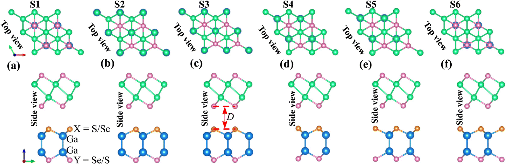 | ||
| Fig. 2 Top view and side view of the γ-GeSe/Ga2SSe heterostructures for six different arrangements of (a) S1, (b) S2, (c) S3, (d) S4, (e) S5 and (f) S6 stacking. | ||
 | ||
| Fig. 3 (a) Calculated binding energies and interlayer spacings in the γ-GeSe/Ga2SSe heterostructures for different arrangements. AIMD simulation of the total energy and temperature of the most energetically favorable arrangement (b) S2 for γ-GeSe/SGa2Se and (c) S6 for γ-GeSe/SeGa2S heterostructure. | ||
Furthermore, to access the stability of the γ-GeSe/Ga2SSe heterostructure, we perform the binding energy calculations as the difference in the total energies of the heterostructure and the isolated monolayers as below:
 | (1) |
The binding energy of the γ-GeSe/Ga2SSe heterostructure for all stacking patterns are depicted in Fig. 3(a). Notably, the binding energy Eb ranges from −10 to −18 meV Å−2. The negative values of the Eb indicate that this heterostructure is stable. Interestingly, the Eb values are comparable with those in other vdW-typical systems, such as graphite,57,58 graphene/InSe59 and MX2 compounds.60 This observation indicates that the γ-GeSe/Ga2SSe heterostructures are mainly governed by physicoadsorption rather than strong chemical bonding. This type of interaction often leads to stable and further support the stability of the heterostructure while allowing for potential flexibility in its properties. For the γ-GeSe/SGa2Se heterostructure, the S2 stacking shows the lowest value of the Eb, specializing that it is the most energetically favorable arrangement. Similarly, in the γ-GeSe/SeGa2S heterostructure, the S6 stacking exhibits the lowest binding energy, signifying that this configuration is the most energetically stable. Hence, the S2 stacking of the γ-GeSe/SGa2Se and S6 stacking of the γ-GeSe/SeGa2S heterostructures will be the focus of subsequent investigations. The ab initio molecular dynamics (AIMD) simulations of the total energy and temperature are performed to access the thermal stability of the most energetically favorable arrangement of the S2 stacking in the γ-GeSe/SGa2Se and S6 stacking in the γ-GeSe/SeGa2S heterostructures. These results of the AIMD simulations are depicted in Fig. 3(b) and (c). Notably, the small variations in total energies and temperatures during the relaxation process suggest that the heterostructures exhibit thermal stability.
We further examine the electronic properties of the γ-GeSe/Ga2SSe heterostructures for various stacking arrangements. The projections of the band structures of the γ-GeSe/SGa2Se heterostructure for six stacking arrangements are illustrated in Fig. 4(a). It can be seen that the γ-GeSe/SGa2Se heterostructure exhibits the semiconducting features with the indirect band gap nature. The VBM is located at the Γ point and the CBM is located along the K–Γ path. The band gap of the γ-GeSe/SGa2Se heterostructure for six stacking arrangements is obtained to be 0.78 eV. This value is smaller than that of the Ga2SSe material, but it is larger than that of the γ-GeSe material. Notably, the indirect band gap characteristic of the heterostructure makes it promising for photodetection and solar energy conversion. Additionally, we observe that the contribution of the γ-GeSe and Ga2SSe layers to the band edges of their heterostructure varies across different stacking arrangements, as indicated by the weighted projections in Fig. 4(a). In all six stacking arrangements of the γ-GeSe/SGa2Se heterostructure, the VBM is dominated by contributions from the γ-GeSe layer, while the CBM is mainly derived from the Ga2SSe layer, specifying the type-II band alignment. This type of alignment is beneficial for applications such as solar cells and photodetectors, where efficient charge separation is crucial.
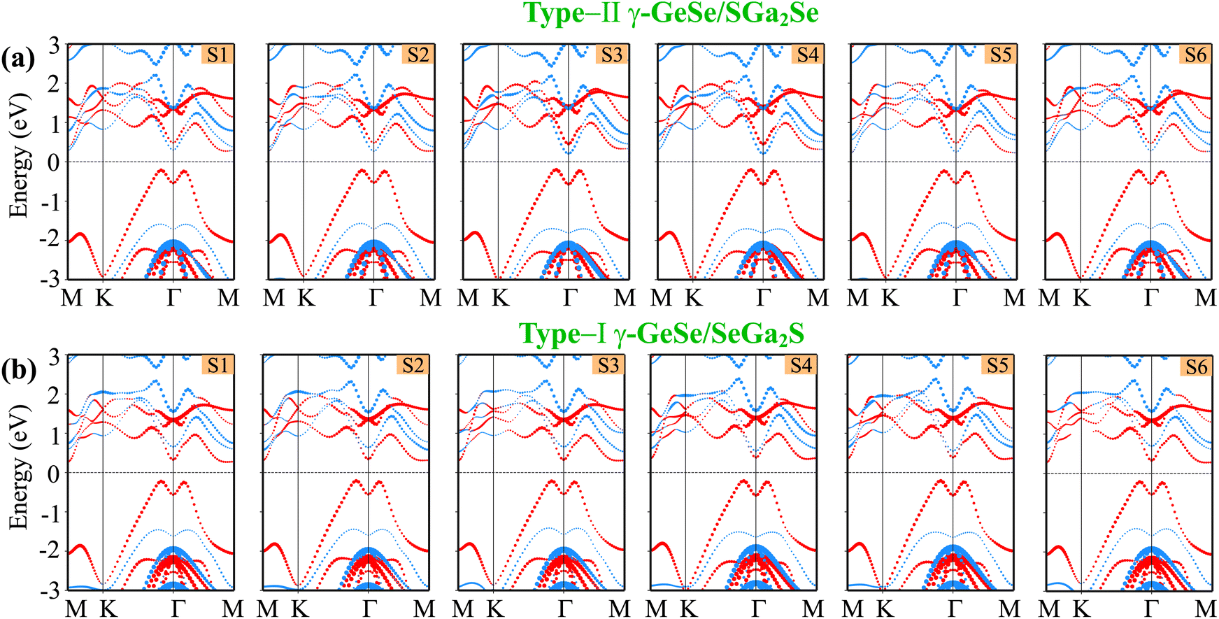 | ||
| Fig. 4 The projections of the band structures for the different stacking arrangements in the (a) γ-GeSe/SGa2Se and (b) γ-GeSe/SeGa2S heterostructures. The projections of the γ-GeSe and Ga2SSe layers are visualized by red and blue lines, respectively. | ||
Similarly, the γ-GeSe/SeGa2S heterostructure also exhibits the semiconducting nature with an indirect band gap, as depicted in Fig. 4(b). In this case, VBM is located at the Γ point, while the CBM is positioned along the Γ–K path. The indirect nature of the band gap can influence the efficiency of optoelectronic devices, potentially lowering their performance in applications like light-emitting diodes (LEDs), but it may still be advantageous for other applications such as thermoelectrics61–63 More interestingly, the γ-GeSe/SeGa2S heterostructure forms a type-I band alignment, where the band edges of the γ-GeSe layer lie within the band edges of the Ga2SSe. It indicates that both the VBM and CBM of the γ-GeSe/SeGa2S heterostructure is mainly contributed by the γ-GeSe layer. One should be pointed out that this type of band alignment is advantageous for optoelectronic applications such as light-emitting diodes (LEDs) and lasers because it efficiently confines both electrons and holes within the same material layer, facilitating enhanced recombination. Hence, type-I band alignment is highly advantageous for light-emitting applications because it traps both electrons and holes in a region where efficient radiative recombination can occur, making it ideal for LEDs, lasers, and other optoelectronic devices that rely on light emission.64,65 The coexistence of both type-I and type-II band alignments in the γ-GeSe/Ga2SSe heterostructure demonstrates the versatility of these materials. By selecting different stacking configurations, it is possible to tailor the electronic and optoelectronic properties of the heterostructure for specific applications, ranging from energy-harvesting devices to light-emitting components.
Furthermore, the charge transfers between the γ-GeSe and Ga2SSe layers are visualized by considering the charge density difference (CDD) as:
| Δρ = ρH − ργ − ρG | (2) |
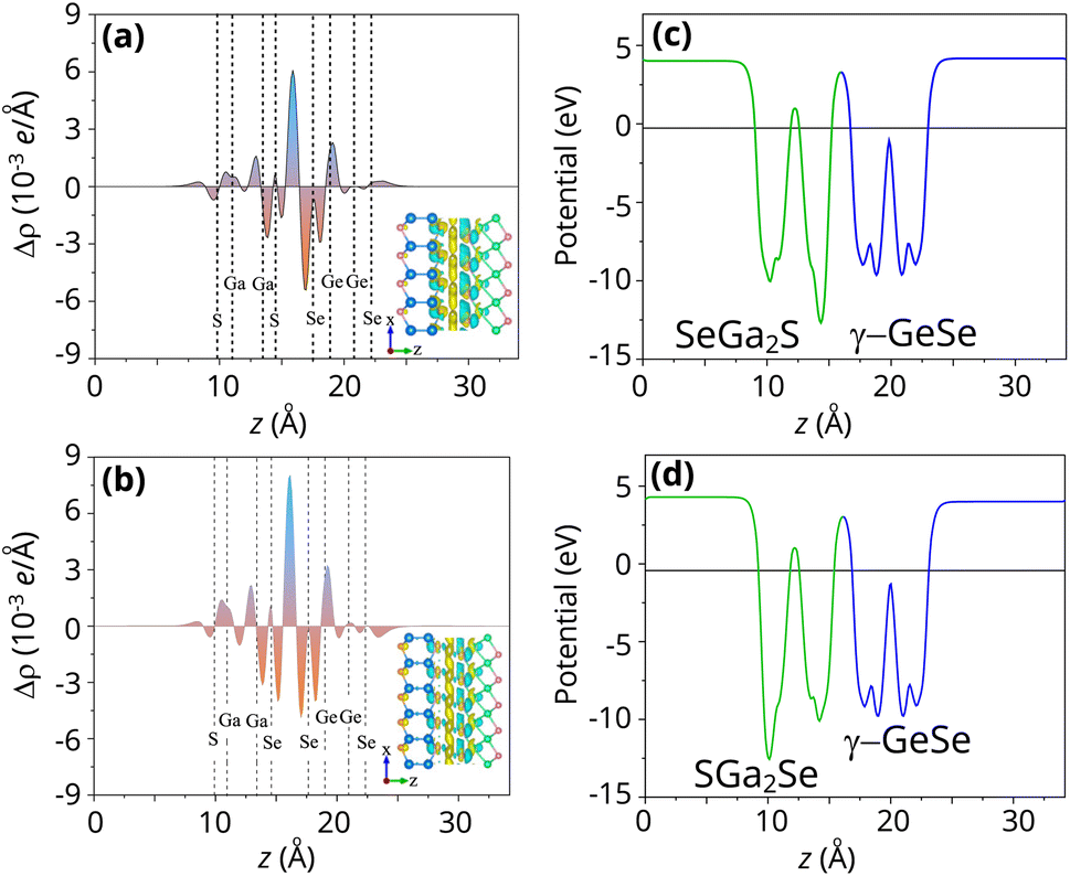 | ||
| Fig. 5 (a) Charge density difference and (c and d) electrostatic potential of the (a and c) γ-GeSe/SGa2Se and (b and d) γ-GeSe/SeGa2S heterostructures. The yellow and cyan areas indicate the positive and negative charges, respectively. | ||
Moreover, the transport properties of the γ-GeSe/Ga2SSe heterostructures are also calculated to confirm their potential applications in next-generation electronic and optoelectronic devices. The carrier mobility of heterostructures can be obtained as follows:
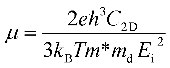 | (3) |
 Ei is the deformation potential for electrons or holes. The carrier mobilities of the γ-GeSe and Ga2SSe monolayers are also calculated for the comparison. Our results demonstrate that the γ-GeSe and Ga2SSe monolayers exhibit high carrier mobilities of approximately 812/421 and 303/141 cm2 V−1 s−1 for electrons/holes, respectively, which align well with previously reported values.14,44 Upon forming the γ-GeSe/Ga2SSe heterostructure, the carrier mobility significantly increases, reaching 2105/709 cm2 V−1 s−1 in the γ-GeSe/SGa2Se configuration and 3217/767 cm2 V−1 s−1 in the γ-GeSe/SeGa2S configuration for electrons/holes. These values of the carrier mobility are comparable with those in other heterostructures, such as BC6N/BN,66 MoSSe/GaN,67 Sb/SnSe68 and GeC(ZnO)/Al2SO69 heterostructures. The enhancement in the carrier mobility suggests that the formation of the γ-GeSe/Ga2SSe heterostructure significantly improves the electronic transport properties, making it highly advantageous for high-performance electronic and optoelectronic applications.
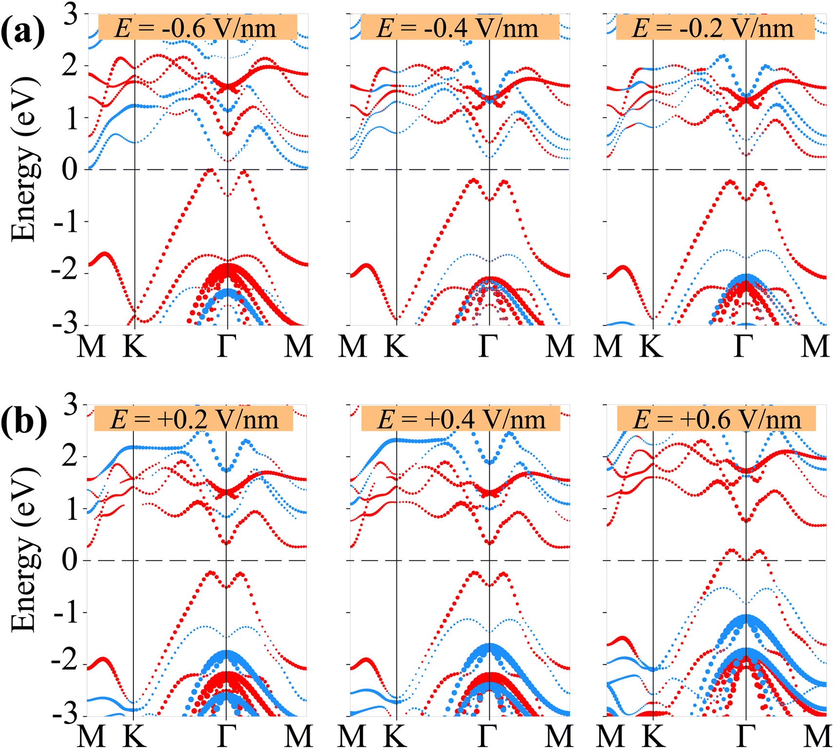
More interestingly, the versatility in the electronic properties of the γ-GeSe/Ga2SSe heterostructure are crucial for the practical application. The ability to modulate band alignments of the heterostructure opens up opportunities for designing multifunctional devices. Therefore, we further investigate the versatility in the electronic properties of the γ-GeSe/Ga2SSe heterostructure under applied electric fields. The variations in the band gap of the γ-GeSe/Ga2SSe heterostructure under applied electric field are presented in Fig. 6. It is evident that the electric fields vary the band gap of the γ-GeSe/Ga2SSe heterostructure and include the transformation between type-I and type-II band alignment. For the γ-GeSe/SGa2Se heterostructure, the negative electric field results in a reduction of the band gap. When a negative electric field of −0.7 V nm−1 is applied, the band gap of the heterostructure reduces to zero, causing a transition from semiconductor to metal. On the contrary, applying a positive electric field initially causes the band gap to increase. However, when the positive electric field exceeds +0.5 V nm−1, a reversal is observed, leading to a gradual decrease in the band gap. When a positive electric field of +0.7 V nm−1 is applied, the band gap of the heterostructure closes, resulting in a transition to a metallic state. The transformation from type-II to type-I is observed in the γ-GeSe/SGa2Se heterostructure under the positive electric field of +0.1 V nm−1. For the γ-GeSe/SeGa2S heterostructure, a similar behavior is observed under an applied electric field. Both negative and positive electric fields drive the transition of the heterostructure from a semiconductor to a metallic state. Specifically, a negative electric field causes a reduction in the band gap, while a positive electric field initially enhances the band gap. However, when the positive electric field exceeds +0.4 V nm−1, the band gap begins to decrease again. Additionally, the application of electric fields not only alters the band gap but also induces a transformation in the band alignment. Under a negative electric field lower than −0.4 V nm−1, the band alignment shifts from type-I to type-II, further emphasizing the tunability of the electronic properties of the heterostructure. This flexibility in adjusting both band gap and band alignment highlights the potential of the γ-GeSe/Ga2SSe heterostructure for multifunctional device applications.
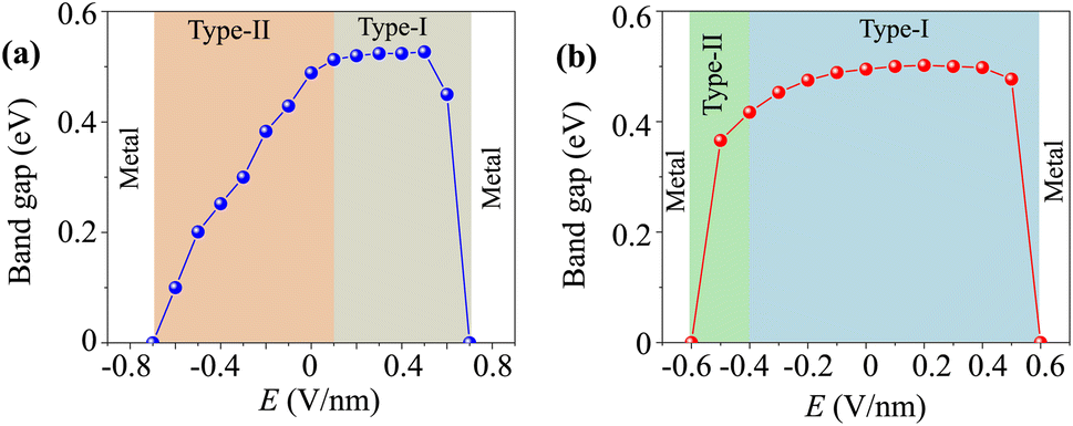 | ||
| Fig. 6 The variation of the band gap of (a) γ-GeSe/SGa2Se and (b) γ-GeSe/SeGa2S heterostructure under applied electric field. | ||
We further analyze the weighted projections of the band structures for both the γ-GeSe/SGa2Se and γ-GeSe/SeGa2S heterostructures under varying strengths of applied electric fields, as shown in Fig. 7 and 8. This detailed investigation reveals the underlying mechanisms responsible for the tunability of the electronic properties. It is evident that the negative electric field induces the shifts in the band edges of the γ-GeSe and Ga2SSe layers in two opposite directions. The band edges of the γ-GeSe shift towards the region with the higher binding energy, while the band edges of the Ga2SSe layer shifts in the opposite direction, i.e. toward the region with the lower binding energy. The shifts are depicted in Fig. 7(a). This observation also supports that the band gap of the γ-GeSe/SGa2Se heterostructure is reduced upon the application of the negative electric field. The band edges of the heterostructure cross the Fermi level under the negative electric field of −0.7 V nm−1, driving the transition from the semiconductor to metal. Similarly, when a positive electric field is applied, the band edges of the two constituent layers shift in opposite directions. Under a positive electric field, the band edges of the γ-GeSe layer shift downward toward lower binding energies, while the band edges of the Ga2SSe layer shift upward toward higher binding energies. This opposing behavior between the layers contributes to further modulation of the electronic properties, including changes in the band gap and type of band alignment. Under the positive electric field exceeded +0.1 V nm−1, the band edges of the γ-GeSe/SGa2Se heterostructure are mainly derived from the γ-GeSe layer, signifying a transformation from type-II to type-I. When a positive electric field of +0.7 V nm−1 is applied, the VBM of the heterostructure crosses the Fermi level, signaling a transition from a semiconductor to a semimetal. The shift in the band alignment of the γ-GeSe/SGa2Se heterostructure, driven by the applied electric field, suggests its potential as a promising candidate for multifunctional devices. The similar shifts in the band edges of the constituent γ-GeSe and Ga2SSe layer under applied electric fields are also observed in the γ-GeSe/SeGa2S heterostructure, as illustrated in Fig. 8. Notably, a transformation from type-I to type-II band alignment occurs under a negative electric field of −0.4 V nm−1. In this scenario, the VBM is dominated by contributions from the γ-GeSe layer, while the CBM originates from the Ga2SSe layer, signifying a clear conversion to type-II band alignment. Furthermore, the band edges of the heterostructure cross the Fermi level at the electric field of E = ±0.6 V nm−1, confirming the transition from semiconductor to metallic state. Therefore, the tunability in electronic properties, particularly the ability to transition between type-I and type-II band alignments in the γ-GeSe/SGa2Se and γ-GeSe/SeGa2S heterostructures, opens up new possibilities for diverse applications, including transistors, photodetectors, and optoelectronic devices.
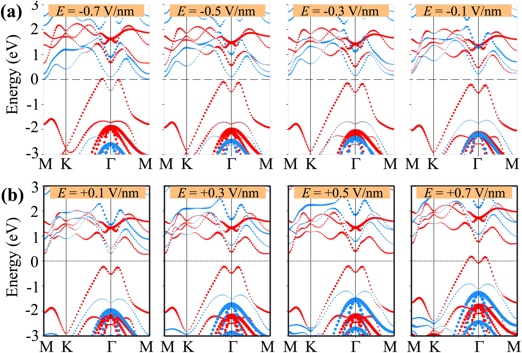 | ||
| Fig. 7 Weighted projections of the band structures of the γ-GeSe/SGa2Se heterostructure under applied (a) negative and (b) positive electric fields. The projections of the γ-GeSe and Ga2SSe layers are presented by the red and blue balls, respectively. | ||
 | ||
| Fig. 8 Weighted projections of the band structures of the γ-GeSe/SeGa2S heterostructure under applied (a) negative and (b) positive electric fields. The projections of the γ-GeSe and Ga2SSe layers are presented by the red and blue balls, respectively. | ||
4 Conclusions
In conclusion, we have systematically explored the electronic properties and contact behavior of the γ-GeSe/Ga2SSe heterostructures using first-principles calculations. Our findings reveal that the heterostructures exhibit tunable electronic characteristics, with both the γ-GeSe/SGa2Se and γ-GeSe/SeGa2S configurations demonstrating semiconducting behavior. Notably, the γ-GeSe/SGa2Se heterostructure forms a type-II band alignment, while the γ-GeSe/SeGa2S heterostructure exhibits a type-I band alignment. The γ-GeSe/Ga2SSe heterostructures demonstrate significantly enhanced carrier mobility compared to their constituent monolayers. The application of an external electric field significantly modulates the band alignment and electronic properties of the heterostructures. A positive electric field induces a transition from type-II to type-I band alignment in the γ-GeSe/SGa2Se heterostructure, while a negative electric field causes the opposite transformation in the γ-GeSe/SeGa2S heterostructure. The versatility in tuning electronic properties underscores the potential of the γ-GeSe/Ga2SSe heterostructures for next-generation multifunctional devices. These findings provide a promising foundation for future research and development in 2D material-based heterostructures, enabling advanced device engineering with enhanced performance and functionality.Data availability
The data that support the findings of this study are available from the corresponding author upon reasonable request.Conflicts of interest
There are no conflicts to declare.Acknowledgements
This research is funded by the Vietnam Ministry of Education and Training under grant no. B2023.DNA.23.References
- P. Miró, M. Audiffred and T. Heine, Chem. Soc. Rev., 2014, 43, 6537–6554 RSC.
- S. Z. Butler, S. M. Hollen, L. Cao, Y. Cui, J. A. Gupta, H. R. Gutiérrez, T. F. Heinz, S. S. Hong, J. Huang and A. F. Ismach, et al. , ACS Nano, 2013, 7, 2898–2926 CrossRef CAS.
- C. Liu, H. Chen, S. Wang, Q. Liu, Y.-G. Jiang, D. W. Zhang, M. Liu and P. Zhou, Nat. Nanotechnol., 2020, 15, 545–557 CrossRef CAS.
- K. S. Novoselov, A. K. Geim, S. V. Morozov, D.-e. Jiang, Y. Zhang, S. V. Dubonos, I. V. Grigorieva and A. A. Firsov, Science, 2004, 306, 666–669 CrossRef CAS PubMed.
- S. Manzeli, D. Ovchinnikov, D. Pasquier, O. V. Yazyev and A. Kis, Nat. Rev. Mater., 2017, 2, 1–15 Search PubMed.
- L. Zheng, X. Wang, H. Jiang, M. Xu, W. Huang and Z. Liu, Nano Res., 2022, 1–20 Search PubMed.
- G. Cassabois, P. Valvin and B. Gil, Nat. Photonics, 2016, 10, 262–266 CrossRef CAS.
- K. K. Kim, A. Hsu, X. Jia, S. M. Kim, Y. Shi, M. Dresselhaus, T. Palacios and J. Kong, ACS Nano, 2012, 6, 8583–8590 CrossRef CAS PubMed.
- A. K. Geim and K. S. Novoselov, Nat. Mater., 2007, 6, 183–191 CrossRef CAS PubMed.
- M. S. Jang, H. Kim, Y.-W. Son, H. A. Atwater and W. A. Goddard III, Proc. Natl. Acad. Sci. U. S. A., 2013, 110, 8786–8789 CrossRef CAS PubMed.
- K. F. Mak, C. Lee, J. Hone, J. Shan and T. F. Heinz, Phys. Rev. Lett., 2010, 105, 136805 CrossRef PubMed.
- Z. Yu, Z.-Y. Ong, S. Li, J.-B. Xu, G. Zhang, Y.-W. Zhang, Y. Shi and X. Wang, Adv. Funct. Mater., 2017, 27, 1604093 CrossRef.
- S. Lee, J.-E. Jung, H.-g. Kim, Y. Lee, J. M. Park, J. Jang, S. Yoon, A. Ghosh, M. Kim and J. Kim, et al. , Nano Lett., 2021, 21, 4305–4313 CrossRef CAS PubMed.
- N. Luo, W. Duan, B. I. Yakobson and X. Zou, Adv. Funct. Mater., 2020, 30, 2000533 CrossRef CAS.
- W. Zhang, Y. Cui, C. Zhu, B. Huang, Y. Lou and S. Yan, Mater. Chem. Phys., 2023, 305, 127964 CrossRef CAS.
- C. Huan, P. Wang, B. He, Y. Cai and Q. Ke, 2D Mater., 2022, 9, 045014 CrossRef CAS.
- H. Minhas, S. Das and B. Pathak, ACS Appl. Energy Mater., 2022, 5, 9914–9928 CrossRef CAS.
- C. Liu, S. Guan, H. Yin, W. Wan, Y. Wang and Y. Zhang, Appl. Phys. Lett., 2019, 115, 252904 CrossRef.
- J. Jang, J. Kim, D. Sung, J. H. Kim, J.-E. Jung, S. Lee, J. Park, C. Lee, H. Bae and S. Im, et al. , Nano Lett., 2023, 23, 3144–3151 CrossRef CAS PubMed.
- J.-E. Jung, S. Lee, H. Kang, M. Jang, J. Park, M. Petri, H. Lipsanen, Z. Sun, H. H. Yoon and K. Kim, J. Mater. Chem. C, 2024, 12, 9662–9668 RSC.
- Z. Shu, X. Cui, B. Wang, H. Yan and Y. Cai, ChemSusChem, 2022, 15, e202200564 CrossRef CAS.
- A.-Y. Lu, H. Zhu, J. Xiao, C.-P. Chuu, Y. Han, M.-H. Chiu, C.-C. Cheng, C.-W. Yang, K.-H. Wei and Y. Yang, et al. , Nat. Nanotechnol., 2017, 12, 744–749 CrossRef CAS PubMed.
- J. Zhang, S. Jia, I. Kholmanov, L. Dong, D. Er, W. Chen, H. Guo, Z. Jin, V. B. Shenoy and L. Shi, et al. , ACS Nano, 2017, 11, 8192–8198 CrossRef CAS PubMed.
- X. Wan, E. Chen, J. Yao, M. Gao, X. Miao, S. Wang, Y. Gu, S. Xiao, R. Zhan and K. Chen, et al. , ACS Nano, 2021, 15, 20319–20331 CrossRef CAS PubMed.
- B. Sa, X. Shen, S. Cai, Z. Cui, R. Xiong, C. Xu, C. Wen and B. Wu, Phys. Chem. Chem. Phys., 2022, 24, 15376–15388 RSC.
- L. Wu, G. Zheng, W. Zhou, D. Zhang, S. Qu, B. Zhang, H. Duan and F. Ouyang, Phys. Lett. A, 2022, 455, 128504 CrossRef CAS.
- S. Yao, X. Ma, C. Huang, Y. Guo, Y. Ren and N. Ma, Mater. Sci. Semicond. Process., 2024, 178, 108367 CrossRef CAS.
- S. Singh and S. Choudhary, Opt. Quant. Electron., 2021, 53, 1–13 CrossRef.
- W. Zhang, J. Hou, M. Bai, C. He and J. Wen, Appl. Surf. Sci., 2023, 634, 157648 CrossRef CAS.
- W. Zhang, Y. Yin and C. He, J. Phys. Chem. Lett., 2021, 12, 5064–5075 CrossRef CAS.
- K. Qin, E. Li, Y. Shen, D. Ma, P. Yuan, H. Wang and Z. Cui, Surf. Interfaces, 2024, 52, 104996 CrossRef CAS.
- K. S. Novoselov, A. Mishchenko, A. Carvalho and A. C. Neto, Science, 2016, 353, aac9439 CrossRef CAS.
- P. V. Pham, S. C. Bodepudi, K. Shehzad, Y. Liu, Y. Xu, B. Yu and X. Duan, Chem. Rev., 2022, 122, 6514–6613 CrossRef CAS PubMed.
- W. Tan, Z.-W. Zhang, X. Zhou, Z.-L. Yu, Y.-Q. Zhao, S. Jiang and Y. S. Ang, Phys. Rev. Mater., 2024, 8, 094414 CrossRef.
- M. Idrees, U. Khan, B. Ali and B. Amin, Appl. Phys. A: Mater. Sci. Process., 2024, 130, 727 CrossRef CAS.
- H. Shu, M. Zhao and M. Sun, ACS Appl. Nano Mater., 2019, 2, 6482–6491 CrossRef CAS.
- Y. Luo, S. Wang, H. Shu, J.-P. Chou, K. Ren, J. Yu and M. Sun, Semicond. Sci. Technol., 2020, 35, 125008 CrossRef CAS.
- K. Ren, W. Tang, M. Sun, Y. Cai, Y. Cheng and G. Zhang, Nanoscale, 2020, 12, 17281–17289 RSC.
- Z. Cui, K. Ren, Y. Zhao, X. Wang, H. Shu, J. Yu, W. Tang and M. Sun, Appl. Surf. Sci., 2019, 492, 513–519 CrossRef CAS.
- C. Huan, P. Wang, B. Liu, B. He, Y. Cai and Q. Ke, J. Mater. Chem. C, 2022, 10, 10995–11004 RSC.
- L. Cao, X. Deng, Z. Tang, G. Zhou and Y. S. Ang, Appl. Phys. Lett., 2022, 121, 113104 CrossRef CAS.
- H. T. Nguyen, M. M. Obeid, A. Bafekry, M. Idrees, T. V. Vu, H. V. Phuc, N. N. Hieu, L. T. Hoa, B. Amin and C. V. Nguyen, Phys. Rev. B, 2020, 102, 075414 CrossRef CAS.
- F. Yang, P. Boulet and M.-C. Record, Int. J. Hydrogen Energy, 2024, 73, 536–546 CrossRef CAS.
- K. D. Pham, RSC Adv., 2022, 12, 31935–31942 RSC.
- P. Giannozzi, S. Baroni, N. Bonini, M. Calandra, R. Car, C. Cavazzoni, D. Ceresoli, G. L. Chiarotti, M. Cococcioni and I. Dabo, et al. , J. Phys.: Condens. Matter, 2009, 21, 395502 CrossRef.
- J. P. Perdew, K. Burke and M. Ernzerhof, Phys. Rev. Lett., 1996, 77, 3865 CrossRef CAS PubMed.
- G. Kresse and D. Joubert, Phys. Rev. B: Condens. Matter Mater. Phys., 1999, 59, 1758 CrossRef CAS.
- S. Grimme, J. Antony, S. Ehrlich and H. Krieg, J. Chem. Phys., 2010, 132, 154104 CrossRef.
- S. Nosé, J. Chem. Phys., 1984, 81, 511–519 CrossRef.
- Z. Shu, B. Wang, X. Cui, X. Yan, H. Yan, H. Jia and Y. Cai, Chem. Eng. J., 2023, 454, 140242 CrossRef CAS.
- Y. Shen, P. Yuan, Z. Yuan, Z. Cui, D. Ma, F. Cheng, K. Qin, H. Wang and E. Li, Int. J. Hydrogen Energy, 2024, 80, 289–297 CrossRef CAS.
- G. Yuan, Z. Cheng, Y. Cheng, W. Duan, H. Lv, Z. Liu, C. Han and X. Ma, ACS Appl. Electron. Mater., 2022, 4, 2897–2905 CrossRef CAS.
- S. T. Nguyen, N. V. Hieu, H. Le-Quoc, K. Nguyen-Ba, C. V. Nguyen, H. V. Phuc and C. Q. Nguyen, Nanoscale Adv., 2024, 6, 3624–3631 RSC.
- S. H. Gul, B. Ali, M. Shafiq, M. Idrees and B. Amin, J. Solid State Chem., 2023, 326, 124187 CrossRef CAS.
- S. Ahmad, H. Din, S. U. Sabir and B. Amin, Nanoscale Adv., 2023, 5, 4598–4608 RSC.
- S. Nguyen, T. Huong, N. Ca and C. Nguyen, Nanoscale Adv., 2024, 6, 1565–1572 RSC.
- S. D. Chakarova-Käck, E. Schröder, B. I. Lundqvist and D. C. Langreth, Phys. Rev. Lett., 2006, 96, 146107 CrossRef.
- Z. Liu, J. Z. Liu, Y. Cheng, Z. Li, L. Wang and Q. Zheng, Phys. Rev. B: Condens. Matter Mater. Phys., 2012, 85, 205418 CrossRef.
- X. Yang, B. Sa, P. Lin, C. Xu, Q. Zhu, H. Zhan and Z. Sun, J. Phys. Chem. C, 2020, 124, 23699–23706 CrossRef CAS.
- T. Björkman, A. Gulans, A. V. Krasheninnikov and R. M. Nieminen, Phys. Rev. Lett., 2012, 108, 235502 CrossRef.
- K. Bashir, M. Bilal, B. Amin, Y. Chen and M. Idrees, RSC Adv., 2023, 13, 9624–9635 RSC.
- H. Rghioui, M. S. Zyane, A. Marjaoui, M. A. Tamerd, M. Diani and M. Zanouni, Phys. E, 2024, 162, 115985 CrossRef CAS.
- O. A. López-Galán, I. Perez, J. Nogan and M. Ramos, Adv. Mater. Interfaces, 2023, 10, 2202339 CrossRef.
- M. Z. Bellus, M. Li, S. D. Lane, F. Ceballos, Q. Cui, X. C. Zeng and H. Zhao, Nanoscale Horiz., 2017, 2, 31–36 RSC.
- Q. Alam, S. Sardar, H. Din, S. Khan, M. Idrees, B. Amin, F. Rehman, S. Muhammad and A. Laref, Nanoscale Adv., 2022, 4, 3557–3565 RSC.
- N. Jiang, Y. Xie, S. Wang, Y. Song, L. Chen, W. Han, X. Jin, Z. Zhou and Z. Yan, Appl. Surf. Sci., 2023, 623, 157007 CrossRef CAS.
- W.-J. Yin, X.-L. Zeng, B. Wen, Q.-X. Ge, Y. Xu, G. Teobaldi and L.-M. Liu, Front. Phys., 2021, 16, 1–9 Search PubMed.
- D. Ahmed, N. Muhammad and Z. Ding, Phys. E, 2025, 165, 116064 CrossRef CAS.
- S. Ahmad, K. Sohail, L. Chen, H. Xu, H. Din and Z. Zhou, Int. J. Hydrogen Energy, 2023, 48, 25354–25365 CrossRef CAS.
| This journal is © The Royal Society of Chemistry 2025 |