 Open Access Article
Electronic and magnetic properties of the HfO2 monolayer engineered by doping with transition metals and nonmetal atoms towards spintronic applications
Nguyen Thi
Han
a,
J.
Guerrero-Sanchez
b and
D. M.
Hoat
 *cd
*cd
aDepartment of Basic Science, Hung Yen University of Technology and Education, Hung Yen, Vietnam
bUniversidad Nacional Autónoma de México, Centro de Nanociencias y Nanotecnología, Apartado Postal 14, Ensenada, Baja California 22800, Mexico
cInstitute of Theoretical and Applied Research, Duy Tan University, Ha Noi 100000, Vietnam. E-mail: dominhhoat@duytan.edu.vn
dFaculty of Natural Sciences, Duy Tan University, Da Nang 550000, Vietnam
First published on 20th November 2024
Abstract
Doping two-dimensional (2D) materials is a vitally important method to modulate their electronic and magnetic properties. In this work, doping with transition metals (TM = Mn and Fe) and nonmetal atoms (X = B and C) is proposed to engineer the magnetism in the HfO2 monolayer. The pristine monolayer is an intrinsically nonmagnetic insulator with a large band gap of 4.85 (6.43) eV as calculated using the PBE (HSE06) functional. Doping with Mn and Fe atoms induces monolayer magnetization with total magnetic moments of 3.00 and 4.00μB, respectively. Herein, Mn- and Fe-3d electrons produce mainly magnetic properties and regulate the electronic nature by forming new mid-gap energy states. Similarly, the 2p orbital of impurities plays a key role in determining the electronic and magnetic properties of B- and C-doped systems. Mn and B doping leads to the emergence of magnetic semiconductor nature, while the half-metallicity is obtained by doping with Fe and C atoms. Further, the substitution of the Hf–O pair with the TM–X pair is also studied. In these cases, both TM and X impurities induce the system magnetism, exhibiting an antiparallel spin orientation. Consequently, pair-atom-doped systems have smaller total magnetic moments in comparison with single-atom-doped systems. Interestingly, doping with all four Mn–B, Mn–C, Fe–B, and Fe–C pairs induces a magnetic semiconductor nature, where spin-dependent energy gaps are determined by the doping-induced multiple mid-gap energy states. When incorporated into the HfO2 monolayer lattice, transition metals lose charge, while nonmetal impurities act as charge gainers. This study demonstrates the effectiveness of the doping method to engineer the magnetism in the HfO2 monolayer for spintronic applications.
1. Introduction
Over the past two decades, researchers have paid immense attention to two-dimensional (2D) materials because of their intriguing and interesting physical and chemical characteristics.1,2 As a pioneering member, graphene is mechanically strong and exhibits high carrier mobility and high electrical and thermal conductivity. These features arise from the unique sp2 hybridization of carbon atoms in the honeycomb-like planar structure.3–5 However, the practical applications of graphene, for example in field-effect transistors (FETs), are considerably hindered because of its semimetal character. Therefore, researchers have investigated effective methods to open the graphene band gap.6,7 Besides, great research attention has also been paid to developing 2D materials beyond graphene, such as silicene,8 phosphorene,9 hexagonal boron nitride (h-BN),10,11 transition metal dichalcogenides (TMDs),12,13 and MXenes (transition metal carbides and nitrides),14,15 among others. In this regard, 2D semiconductors have emerged as promising candidates to fabricate high-performance 2D FETs, whose intrinsic band gap may lead to a high on/off ratio.16,17 Moreover, these materials have also been explored as promising candidates for diverse applications, such as optoelectronics18–20 and photovoltaics.21,22 In this regard, 2D hafnium dichalcogenides HfX2 (X = S and Se) – as members of the transition metal dichalcogenide (TMD) family – have been widely investigated. Experimentally, 2D HfX2 and ternary HfS2(1−x)Se2x can be fabricated by either a top-down method (exfoliation from HfX2 bulk compounds)23,24 or a bottom-up method (chemical vapor deposition – CVD).25–27 Theoretical calculations confirm their semiconductor nature with an energy gap in the visible range, demonstrating their potential for light harvesting,28,29 which can be effectively tuned through external strain.30–32 Consequently, HfX2 are prospective 2D platforms for applications in thermoelectrics,33,34 optoelectronics,35,36 gas sensing,37,38 and spintronics,39,40 among others.Stimulated by the success of 2D TMDs, 2D transition metal dioxides have also been investigated by several groups. For instance, first-principles calculations performed by Zeng et al.41 have confirmed the indirect-gap semiconductor nature of MoO2 and WO2 monolayers, whose energy gaps are smaller than those of MoX2 and WX2 counterparts. The unique photocatalytic properties of MoO2/WO2 vertical heterostructures have also been demonstrated by Chen et al.42 A direct band gap of ∼1.71 eV is found for the most favorable stacking configuration, such that the studied 2D heterostructure has remarkable responses in the visible regime as confirmed by the calculated optical absorption spectra. The electronic and optical properties of the ZrO2 monolayer and bilayers have been studied by Zhang et al.43 Calculations provide large energy gaps of 7.51 and 6.82 eV, respectively. Interestingly, 2D ZrO2 has a larger static dielectric constant compared to the hexagonal boron nitride (h-BN) monolayer, suggesting its promise for FET applications.
HfO2 has been considered as a high dielectric constant (high-κ) material that can be used in the gate dielectric layer in transistors because of its large static dielectric constant. Insights into the interfacial interactions and charge transfer between MoS2 and HfO2 have been provided both experimentally and theoretically.44,45 It is important to mention that the surface states of HfO2 normally affect the transistor performance. Theoretically, Weng et al.46 investigated the HfO2 monolayer using first-principles calculations. The results demonstrate the stability of the 1T phase with a semiconductor gap of 6.73 eV, while the 2H structure is dynamically unstable. After revising the literature, we realize that deep insights into the electronic properties of the HfO2 monolayer are still lacking. Moreover, functionalizing this 2D material through doping in order to expand its applications has not been considered. Previously, 3d transition metals have been selected as impurities to induce magnetism in 2D materials, which is derived from their unpaired 3d orbital.47,48 On the other hand, doping with nonmetal atoms has also been proven to be an effective approach to developing new d0 2D materials.49,50 In this work, the electronic and magnetic properties of the HfO2 monolayer under the effects of doping with transition metals (TM = Mn and Fe) and light atoms (X = B and C), as well as TM–X pair atoms, are systematically investigated. It is anticipated that the HfO2 monolayer is intrinsically nonmagnetic. The proposed doping induces significant magnetism in the HfO2 monolayer, with the doped systems exhibiting diverse feature-rich electronic properties suitable for spintronic applications.
2. Computational details
Under the framework of density functional theory (DFT),51 this paper uses the Vienna Ab initio Simulation Package (VASP)52,53 to realize spin-polarized first-principles calculations on the electronic and magnetic characteristics of pristine and doped HfO2 monolayers. Electron exchange–correlation potentials in the self-consistent iterations are treated using the PBE version (Perdew–Burke–Ernzerhof) of the generalized gradient approximation (GGA-PBE).54 The projector augmented wave (PAW) method describes the interactions between valence electrons and nuclei. In addition, DFT corrected by a Hubbard term proposed by Dudarev et al.55 is also adopted to account for the strong electronic correlations in Mn- and Fe-3d orbitals. Herein, effective Hubbard parameters Ueff of 3.90 and 5.40 eV are employed, which have produced reasonable results in previous studies.56 A cutoff energy of 500 eV is set to truncate the plane wave basis set. The structure is optimized when residual force acting on each atom is found to be less than 0.01 eV Å−1. In all calculations, the criterion of convergence is set to 10−6 eV for total system energy. A 20 × 20 × 1 Monkhorst–Pack k-point grid57 is constructed when integrating the Brillouin zone of the unit cell. In the process of investigating the effects of doping, a 4 × 4 × 1 supercell model containing 48 atoms (16 Hf atoms and 32 O atoms) is constructed, for which a 4 × 4 × 1 k-mesh is generated to sample the Brillouin zone. All structure models are built with a vacuum thickness of more than 14 Å to avoid interlayer interactions.3. Results and discussion
3.1. Pristine HfO2 monolayer
So far, binary 2D materials with 1![[thin space (1/6-em)]](https://www.rsc.org/images/entities/char_2009.gif) :
:![[thin space (1/6-em)]](https://www.rsc.org/images/entities/char_2009.gif) 2 stoichiometry have been found in 1T,58,59 1T′,60,61 and 2H structures.62,63 Herein, the 1T structure is adopted to predict the HfO2 monolayer that is inspired by HfS2 and HfSe2 monolayers.28Fig. 1a shows a unit cell of this 2D material, containing one formula unit. From the structural optimization, the unit cell of the HfO2 monolayer has the following parameters: (1) lattice constant a = 3.24 Å, which is smaller than that of HfS2 and HfSe2 monolayers according to the reduction of this parameter when decreasing the atomic number of VIA-group atoms;64 (2) chemical bond length dHf–O = 2.11 Å; (3) interatomic angles ∠HfOHf = 100.55° and ∠OHfO = 79.45°; and (4) total buckling height Δt = 2 × ΔO–Hf = 2 × 0.97 = 1.94 Å.
2 stoichiometry have been found in 1T,58,59 1T′,60,61 and 2H structures.62,63 Herein, the 1T structure is adopted to predict the HfO2 monolayer that is inspired by HfS2 and HfSe2 monolayers.28Fig. 1a shows a unit cell of this 2D material, containing one formula unit. From the structural optimization, the unit cell of the HfO2 monolayer has the following parameters: (1) lattice constant a = 3.24 Å, which is smaller than that of HfS2 and HfSe2 monolayers according to the reduction of this parameter when decreasing the atomic number of VIA-group atoms;64 (2) chemical bond length dHf–O = 2.11 Å; (3) interatomic angles ∠HfOHf = 100.55° and ∠OHfO = 79.45°; and (4) total buckling height Δt = 2 × ΔO–Hf = 2 × 0.97 = 1.94 Å.
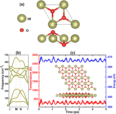 | ||
| Fig. 1 (a) Atomic structure in a unit cell, (b) phonon dispersion curves, and (c) AIMD simulations at 300 K (inset final atomic structure in the 4 × 4 × 1 supercell of the HfO2 monolayer). | ||
After the structural optimization, the monolayer stability is examined as the next step of prediction using the following criteria: (1) phonon spectra of the HfO2 monolayer are recorded using the finite displacement method that is implemented using the PHONOPY code.65 It is well known that the monolayer is dynamically stable if there are no imaginary frequencies in its phonon spectra. In Fig. 1b, phonon dispersion curves of the HfO2 monolayer are plotted along the Γ–M–K–Γ path. Note that no fictitious frequencies appear in the displayed spectra, indicating that the HfO2 monolayer is dynamically stable; (2) ab initio molecular dynamics (AIMD) are performed to verify the thermal stability of the HfO2 monolayer at room temperature, 300 K. The canonical ensemble and Nose–Hooever thermostat66,67 are utilized to control the temperature. A total time of 5 ps is recorded with a time step of 5.0 fs. From Fig. 1c, one can see insignificant fluctuations of temperature and energy during the simulation. In addition, the visualized final structure confirms the integrity of the hexagonal configuration without any broken chemical bonds. These results confirm that the HfO2 monolayer is thermally stable; (3) two independent elastic constants C11 and C12 are calculated for the HfO2 monolayer hexagonal structure to examine the mechanical stability, which is required to meet the following Born's criteria:68C11 > 0 and C11 > |C12|. Our calculations provide values of 173.40 and 41.72 N m−1 for C11 and C12 elastic constants, respectively. Note that these values satisfy Born's criteria, confirming that the HfO2 monolayer is mechanically stable.
The electronic band structure of the HfO2 monolayer is calculated using PBE and hybrid HSE06 functionals. The PBE functional provides a good description of the band structure to determine the material electronic nature; however, it tends to underestimate the electronic band gap. This issue can be overcome with advanced levels of theory, where the hybrid HSE06 functional is a common and widely employed method when including a 25% fraction of the exact Hartree exchange potential.69 The results plotted in Fig. 2a evidence the indirect gap of the HfO2 monolayer since the band edges occur at different locations. Specifically, the valence band maximum and conduction band minimum are located along the ΓK path and at the M point, respectively. PBE and HSE06 calculations yield energy gaps of 4.85 and 6.43 eV, respectively. The large energy gaps confirm the insulating nature of the HfO2 monolayer. The projected density of states (PDOS) given in Fig. 2b indicate the key role of O-px,y,z states in building the valence band, while the conduction band is formed mainly by Hf-dxy–dyz–dz2–dxz–dx2 states. The PDOS profile may suggest the occupied outermost O-2p orbital and unoccupied outermost Hf-5d orbital, suggesting the charge transfer from the Hf atom to O atoms. To confirm this expectation, Bader charge analysis is carried out. It is found that the Hf atom loses a charge quantity of 2.32e, transferring to O atoms (each O atom attracts a charge amount of 1.16e). The charge transfer is also confirmed by the electron localization function visualized in Fig. 2c, where one can see large charge density concentrated at O atoms. Consequently, it can be concluded that the Hf–O chemical bond in the HfO2 monolayer is predominantly ionic, which is generated by the charge transfer from the Hf (less electronegative) atom to O (more electronegative) atoms.
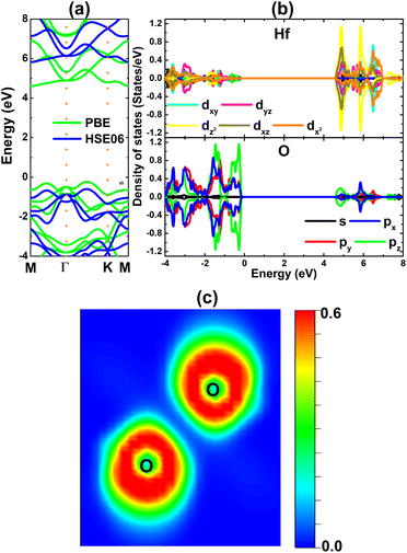 | ||
| Fig. 2 (a) Electronic band structure (the Fermi level is set to 0 eV), (b) projected density of states, and (c) electron localization function of the HfO2 monolayer. | ||
3.2. Effects of doping with Mn and Fe atoms in the Hf sublattice
In this part, doping with transition metals (TMs = Mn and Fe) in the Hf sublattice is proposed to induce novel electronic and magnetic features in the HfO2 monolayer. MnHf and FeHf notations are employed to denote Mn- and Fe-doped HfO2 monolayers, respectively. Firstly, the formation energy Ef and cohesive energy Ec of MnHf and FeHf systems are calculated using the following expressions:| Ef = E(TMHf) − E(HfO2) + μHf − μTM | (1) |
 | (2) |
| E f | E c | E g | ΔQ | M t | |
|---|---|---|---|---|---|
| MnHf | 5.84 | −7.65 | 3.88/1.99 | +1.78 | 3.00 |
| FeHf | 7.02 | −7.66 | M/3.40 | +1.79 | 4.00 |
| BO | 9.39 | −7.74 | 2.42/3.38 | −0.82 | 3.00 |
| CO | 9.28 | −7.78 | 3.80/M | −1.01 | 2.00 |
| MnHfBO | 6.94 | −7.55 | 2.57/0.66 | +1.08/−0.10 | 2.00 |
| MnHfCO | 6.66 | −7.59 | 2.30/3.64 | +1.42/−0.56 | 1.00 |
| FeHfBO | 7.02 | −7.58 | 2.07/2.46 | +0.65/−0.23 | 1.00 |
| FeHfCO | 7.08 | −7.61 | 1.38/3.19 | +1.35/−0.36 | 2.00 |
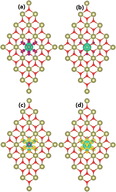
Our spin-polarized calculations evidence the magnetization of the HfO2 monolayer upon doping with Mn and Fe atoms, which is confirmed by the difference between spin-dependent charge densities (ρ↑ − ρ↓). Specifically, total magnetic moments of 3.00 and 4.00μB are obtained for MnHf and FeHf systems, respectively. Fig. 3a and b visualize the spin density in these systems. From the figure, it can be concluded that Mn and Fe impurities produce mainly magnetic properties of MnHf and FeHf systems, respectively, considering their large spin surfaces. Note that six nearest neighboring O atoms also make small contributions to the magnetism, which exhibit an antiparallel spin coupling with transition metal impurities. The electronic interactions between dopant atoms and the host HfO2 monolayer are studied using the charge density difference, which is defined as Δρ = ρ(TMHf) − ρ(HfO2) − ρ(TM), where ρ(TMHf), ρ(HfO2), and ρ(TM) are the charge density of the TM-doped HfO2 monolayer, the bare HfO2 monolayer, and a single TM atom, respectively. From Fig. 3c and d, one can see that Mn and Fe atoms deplete charge, while charge density is increased at O atoms around doping sites. Further, the Bader charge of impurities is analyzed, which confirms that Mn and Fe impurities lose charge quantities of 1.78 and 1.79e, respectively. The charge transfer from Mn and Fe atoms to the host monolayer is a result of their metallic nature, which are surrounded by O atoms, which are much more electronegative atoms. It is important to mention that the charge transfer from Hf to O is more than that from Mn and Fe atoms. This result is derived from the smaller electronegativity of the Hf atom compared to Mn and Fe atoms,70 indicating that the Hf atom has a higher ability to transfer charge.
Fig. 4 shows the calculated spin-polarized band structure and projected density of states (PDOS) of MnHf and FeHf systems. Importantly, mid-gap flat energy states can be noted, which determine their electronic nature. Specifically, new states appear above the Fermi level in both spin channels of the MnHf system, such that it can be classified as a 2D magnetic semiconductor. In this case, spin-up and spin-down states have energy gaps of 3.88 and 1.99 eV, respectively. Furthermore, half-metallicity is induced in the HfO2 monolayer upon doping with Fe atoms, a desirable feature for spintronic applications,71 where the electronic band structure of the FeHf system consists of a metallic spin-up state and semiconductor spin-down state with a band gap of 3.40 eV. PDOS spectra indicate that new energy states in both spin configurations originate mainly from the 3d orbital of Mn and Fe impurities, while the O-2p orbital forms mainly the valence band as observed in the bare monolayer. Note that O-px,y states make a small contribution to the formation of the flat spin-down state at around 1.80 eV of the MnHf system. Moreover, O-px,y states hybridize with Fe-dxy–dyz–dxz–dz2 states to cause the metallic character of the spin-up state. The spin symmetric PDOS of Mn and Fe impurities supports previous conclusions on their key role in producing the magnetic properties of MnHf and FeHf systems, respectively. These results suggest MnHf and FeHf systems as promising 2D spintronic materials,72 indicating the successful functionalization of HfO2 towards spintronic applications.
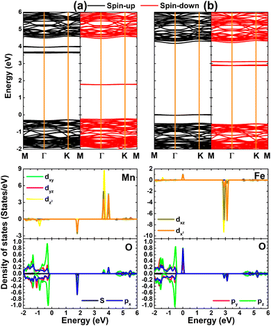 | ||
| Fig. 4 Spin-polarized band structure (the Fermi level is set to 0 eV) and projected density of states of Mn/Fe impurities and their neighboring O atoms in (a) Mn- and (b) Fe-doped HfO2 monolayers. | ||
3.3. Effects of doping with B and C atoms in the O sublattice
Herein, the effects of doping with nonmetal X atoms (X = B and C) in the O sublattice of the HfO2 monolayer are investigated. The doped HfO2 systems are denoted by XO, whose formation energy Ef and cohesive energy Ec are computed as follows:| Ef = E(XO) − E(HfO2) + μO − μX | (3) |
 | (4) |
The obtained results are listed in Table 1. Note that additional energies of 9.39 and 9.29 eV are needed to form BO and CO systems from the HfO2 monolayer through the doping process, respectively. After their formation, the compound state of both systems is energetically more favorable than that of the decomposed state since they have negative Ec values of −7.74 and −7.78 eV per atom, respectively. These results suggest good structural and chemical stability of BO and CO systems, respectively.
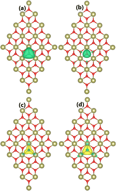
Our calculations confirm the unbalanced charge distribution between the spin channels of the HfO2 monolayer induced by doping with B and C atoms, confirming the appearance of d0 magnetism. Total magnetic moments of 3.00 and 2.00μB are obtained for BO and CO systems, respectively. Note that these values correspond to the difference in valence electrons between O atoms and impurities. From the spin density visualized in Fig. 5a and b for BO and CO systems, it can be concluded that magnetic properties are produced mainly by B and C impurities, respectively, considering their large spin surfaces. After incorporated into the HfO2 sublattice, B and C atoms act as charge gainer atoms since they are surrounded by the less electronegative Hf atoms. The feature is confirmed by the charge density difference illustrated in Fig. 5c and d, which is defined as Δρ = ρ(XO) − ρ(HfO2) − ρ(X). From the figure, the charge enrichment at B and C sites is observed. Because of their smaller electronegativity compared to the O atom,73 B and C atoms gain smaller charge quantities. Specifically, the Bader charge analysis implies that B and C impurities attract charge amounts of 0.82 and 1.01e from the host monolayer, respectively.
The unbalanced charge distribution between the spin channels of BO and CO systems is also reflected in their spin-polarized band structures displayed in Fig. 6. Note that the monolayer spin symmetry is broken with the appearance of mid-gap energy states in both spin configurations, such that they determine the electronic nature of the doped systems. Specifically, both spin-up and spin-down states of the BO system exhibit semiconductor character with energy gaps of 2.42 and 3.38 eV, respectively. The semiconductor spin-up state is also obtained for the CO system with a band gap of 3.80 eV, while the spin-down state is metallized. These results indicate the magnetic semiconductor nature of the BO system and the half-metallic nature of the CO system, which are desirable for spintronic applications.74 Doping the HfO2 monolayer with B and C atoms facilitates the formation of new d0 2D magnetic materials suitable for spintronic applications. To further analyze the effects of doping, PDOS spectra of nonmetal impurities and their neighboring Hf atoms are also given in Fig. 6. Note that flat energy curves observed for the B(C)O system originate mainly from B(C)-px,y states (lower energy states) and the B(C)-pz state (higher energy state), where a smaller contribution from the Hf-5d orbital is also noted. From all the presented analyses, it can be concluded that the electronic and magnetic properties of BO and CO systems are regulated prominently by the outermost B-2p and C-2p orbitals, respectively.
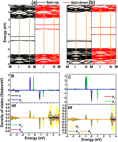 | ||
| Fig. 6 Spin-polarized band structure (the Fermi level is set to 0 eV) and projected density of states of B/C impurities and their neighboring Hf atoms in (a) B- and (b) C-doped HfO2 monolayers. | ||
3.4. Effects of doping with pair atoms
Now, the effects of doping with TM–X pair atoms on the HfO2 monolayer electronic and magnetic properties are investigated. The doped systems are denoted by TMHfXO, which are formed by replacing Hf–O pair atoms with TM–X pair atoms. As a first step, the formation energy Ef and cohesive energy Ec of TMHfXO systems are estimated using the following formulae: | (5) |
 | (6) |
The results are listed in Table 1, which confirm that additional energies of 6.94, 6.66, 7.02, and 7.08 eV per atom are required to realize the processes of doping with Mn–B, Mn–C, Fe–B, and Fe–C pairs, respectively. Once formed, the structures of all four MnHfBO, MnHfCO, FeHfBO, and FeHfCO systems are stabilized, which are suggested by their negative Ec values between −7.61 and −7.55 eV per atom to confirm their structural and chemical stability.
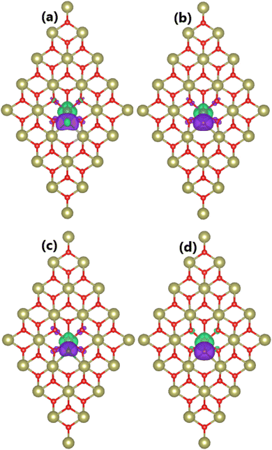
Doping with TM–X pair atoms is proven to induce significant magnetism in the HfO2 monolayer. In this regard, total magnetic moments of 1.00 and 2.00μB are obtained for MnHfCO–FeHfBO and MnHfBO–FeHfCO systems, respectively. Note that these values are smaller than those of the cases of doping with single atoms. To study the magnetic properties in more detail, the spin density of all four systems is visualized in Fig. 7. From the figure, quite similar features can be observed: (1) large spin surfaces indicate that transition metals and nonmetal impurities mainly produce the system magnetism, where the contribution from their neighboring is quite small; (2) importantly, transition metals and nonmetal atoms exhibit antiparallel spin coupling, which is the main reason for the small total magnetic moments of TMHfXO systems. Similar to previous cases, Mn/Fe and B/C atoms act as charge losers and charge gainers, respectively. Specifically, the effective Bader charges of +1.08/−0.10, +1.42/−0.56, +0.65/−0.23, and +1.35/−0.36e are obtained for Mn/B, Mn/C, Fe/B, and Fe/C atoms, respectively. Consequently, it is determined that Mn–B, Mn–C, Fe–B, and Fe–C pairs transfer charge quantities of 0.98, 0.86, 0.42, and 0.99e to the host monolayer, respectively.
Fig. 8 shows the spin-polarized band structures of TMHfXO systems. The appearance of multiple mid-gap flat energy branches in both spin channels can be seen. Importantly, they occur at both above and below the Fermi level to determine the semiconductor character of both spin states. Specifically, spin-up/spin-down energy gaps of 2.57/0.66, 2.30/3.64, 2.07/2.46, and 1.38/3.19 eV are obtained for MnHfBO, MnHfCO, FeHfBO, and FeHfCO systems, respectively. Consequently, these systems can be classified as magnetic semiconductors with antiparallel spin, making them suitable for spintronic applications.
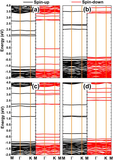 | ||
| Fig. 8 Spin-polarized band structure (the Fermi level is set to 0 eV) of the HfO2 monolayer doped with (a) MnB, (b) MnC, (c) FeB, and (d) FeC pair atoms. | ||
The atom-decomposed DOS spectra of transition metals and nonmetal impurities are displayed in Fig. 9. Focusing on the mid-gap states, it can be noted that they originate from both impurities, supporting the conclusion of their key role in producing the system magnetism as well as regulating the system magnetic semiconductor nature.
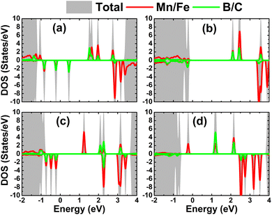 | ||
| Fig. 9 Total and atom-decomposed density of states of impurities of the HfO2 monolayer doped with (a) MnB, (b) MnC, (c) FeB, and (d) FeC pair atoms. | ||
4. Conclusions
In summary, first-principles calculations have been performed to investigate the effects of doping with transition metals and nonmetal atoms on the electronic and magnetic properties of the HfO2 monolayer. The good dynamical, thermal, and mechanical stability of the HfO2 monolayer has been confirmed. This 2D monolayer is a nonmagnetic insulator with a large band gap, whose Hf–O chemical bond is predominantly ionic as a result of charge transfer from the Hf to the O atom. Doping with Mn/Fe atoms in the Hf sublattice and with B/C atoms in the O sublattice induces significant monolayer magnetization with total magnetic moments between 2.00 and 4.00μB. In these cases, PDOS spectra confirm that the electronic and magnetic properties are determined by the 3d orbital of Mn/Fe atoms and the 2p orbital of B/C atoms since they form the mid-gap states around the Fermi level with a strongly unbalanced distribution between spin channels. Being surrounded by O atoms, Mn and Fe transition metals transfer charge quantities of 1.78 and 1.79e to the host monolayer, respectively. In contrast, B and C impurities attract charge amounts of 0.80 and 1.01e from the host monolayer, respectively. The half-metallicity is obtained for FeHf and CO systems, while MnHf and BO systems are proven to be 2D magnetic semiconductors. Further, it is found that the semiconductor nature is also induced by doping with TM–X pairs, which is regulated by multiple mid-gap states. Importantly, TM and X atoms exhibit antiparallel spin coupling, which mainly produces the system magnetism. Bader charge analysis also confirms that the host monolayer gains charge from the incorporated pairs because the lost charge quantity of the TM atom is larger than the gained charge amount of the X atom. Our results provide evidence of the insulating nature of the HfO2 monolayer. Further, doping approaches are proposed to functionalize the HfO2 monolayer towards spintronic applications considering the appearance of desirable electronic and magnetic features.Data availability
Data related to this study are available upon reasonable request.Conflicts of interest
The authors declare that they have no known competing financial interests or personal relationships that could have appeared to influence the work reported in this paper.Acknowledgements
Calculations were performed at the DGCTIC-UNAM Supercomputing Center (projects LANCAD-UNAM-DGTIC-368). D. M. Hoat expresses his gratitude to all the valuable support from Duy Tan University, which is going to celebrate its 30th anniversary of establishment (Nov. 11, 1994–Nov. 11, 2024) towards “Integral, Sustainable and Stable Development”.References
- A. Gupta, T. Sakthivel and S. Seal, Prog. Mater. Sci., 2015, 73, 44–126 CrossRef CAS.
- P. Miró, M. Audiffred and T. Heine, Chem. Soc. Rev., 2014, 43, 6537–6554 RSC.
- K. S. Novoselov, A. K. Geim, S. V. Morozov, D.-E. Jiang, Y. Zhang, S. V. Dubonos, I. V. Grigorieva and A. A. Firsov, science, 2004, 306, 666–669 CrossRef CAS PubMed.
- A. H. Castro Neto, F. Guinea, N. M. Peres, K. S. Novoselov and A. K. Geim, Rev. Mod. Phys., 2009, 81, 109–162 Search PubMed.
- D. Abergel, V. Apalkov, J. Berashevich, K. Ziegler and T. Chakraborty, Adv. Phys., 2010, 59, 261–482 Search PubMed.
- P. Rani and V. Jindal, RSC Adv., 2013, 3, 802–812 Search PubMed.
- M. Y. Han, B. Özyilmaz, Y. Zhang and P. Kim, Phys. Rev. Lett., 2007, 98, 206805 Search PubMed.
- L. Tao, E. Cinquanta, D. Chiappe, C. Grazianetti, M. Fanciulli, M. Dubey, A. Molle and D. Akinwande, Nat. Nanotechnol., 2015, 10, 227–231 CrossRef CAS PubMed.
- L. Li, Y. Yu, G. J. Ye, Q. Ge, X. Ou, H. Wu, D. Feng, X. H. Chen and Y. Zhang, Nat. Nanotechnol., 2014, 9, 372–377 CrossRef CAS PubMed.
- M. J. Molaei, M. Younas and M. Rezakazemi, ACS Appl. Electron. Mater., 2021, 3, 5165–5187 Search PubMed.
- K. K. Kim, A. Hsu, X. Jia, S. M. Kim, Y. Shi, M. Hofmann, D. Nezich, J. F. Rodriguez-Nieva, M. Dresselhaus and T. Palacios, et al. , Nano Lett., 2012, 12, 161–166 Search PubMed.
- M. Chhowalla, Z. Liu and H. Zhang, Chem. Soc. Rev., 2015, 44, 2584–2586 Search PubMed.
- T. Chowdhury, E. C. Sadler and T. J. Kempa, Chem. Rev., 2020, 120, 12563–12591 CrossRef CAS.
- Y. Wei, P. Zhang, R. A. Soomro, Q. Zhu and B. Xu, Adv. Mater., 2021, 33, 2103148 CrossRef CAS.
- B. Anasori, M. Naguib and G. Editors, MRS Bull., 2023, 48, 238–244 CrossRef CAS.
- M. Chhowalla, D. Jena and H. Zhang, Nat. Rev. Mater., 2016, 1, 1–15 Search PubMed.
- X. Jing, Y. Illarionov, E. Yalon, P. Zhou, T. Grasser, Y. Shi and M. Lanza, Adv. Funct. Mater., 2020, 30, 1901971 CrossRef CAS.
- K. F. Mak and J. Shan, Nat. Photonics, 2016, 10, 216–226 Search PubMed.
- S. Kang, D. Lee, J. Kim, A. Capasso, H. S. Kang, J.-W. Park, C.-H. Lee and G.-H. Lee, 2D Materials, 2020, 7, 022003 Search PubMed.
- M. Demirtas, B. Ozdemir, Y. Mogulkoc and E. Durgun, Phys. Rev. B, 2020, 101, 075423 Search PubMed.
- S. Das, D. Pandey, J. Thomas and T. Roy, Adv. Mater., 2019, 31, 1802722 Search PubMed.
- M. Buscema, J. O. Island, D. J. Groenendijk, S. I. Blanter, G. A. Steele, H. S. van der Zant and A. Castellanos-Gomez, Chem. Soc. Rev., 2015, 44, 3691–3718 RSC.
- T. Kanazawa, T. Amemiya, A. Ishikawa, V. Upadhyaya, K. Tsuruta, T. Tanaka and Y. Miyamoto, Sci. Rep., 2016, 6, 22277 CrossRef CAS PubMed.
- H. Kaur, S. Yadav, A. K. Srivastava, N. Singh, S. Rath, J. J. Schneider, O. P. Sinha and R. Srivastava, Nano Res., 2018, 11, 343–353 CrossRef CAS.
- D. Wang, X. Zhang, G. Guo, S. Gao, X. Li, J. Meng, Z. Yin, H. Liu, M. Gao and L. Cheng, et al. , Adv. Mater., 2018, 30, 1803285 CrossRef.
- R. Yue, A. T. Barton, H. Zhu, A. Azcatl, L. F. Pena, J. Wang, X. Peng, N. Lu, L. Cheng and R. Addou, et al. , ACS Nano, 2015, 9, 474–480 CrossRef CAS.
- D. Wang, X. Zhang, H. Liu, J. Meng, J. Xia, Z. Yin, Y. Wang, J. You and X.-M. Meng, 2D Materials, 2017, 4, 031012 CrossRef.
- Q. Zhao, Y. Guo, K. Si, Z. Ren, J. Bai and X. Xu, Phys. Status Solidi B, 2017, 254, 1700033 CrossRef.
- Q.-Y. Chen, M.-Y. Liu, C. Cao and Y. He, Phys. E Low-dimens. Syst. Nanostruct., 2019, 112, 49–58 CrossRef CAS.
- D. Hoat, R. Ponce-Pérez, T. V. Vu, J. Rivas-Silva and G. H. Cocoletzi, Optik, 2021, 225, 165718 CrossRef CAS.
- J. Bao, G. Liu, L. Yang, F. Li, Z. Yang and G. Zhang, Chin. J. Phys., 2024, 89, 1415–1430 CrossRef CAS.
- J. Bao, G. Liu, L. Yang, F. Li, Z. Yang and G. Zhang, Mater. Today Commun., 2024, 39, 108962 Search PubMed.
- G. Ding, G. Gao, Z. Huang, W. Zhang and K. Yao, Nanotechnology, 2016, 27, 375703 CrossRef.
- G. Özbal, R. T. Senger, C. Sevik and H. Sevinçli, Phys. Rev. B, 2019, 100, 085415 CrossRef.
- D. Singh and R. Ahuja, ACS Appl. Energy Mater., 2019, 2, 6891–6903 CrossRef CAS.
- M. Mattinen, G. Popov, M. Vehkamaki, P. J. King, K. Mizohata, P. Jalkanen, J. Raisanen, M. Leskela and M. Ritala, Chem. Mater., 2019, 31, 5713–5724 CrossRef CAS.
- W. Hou, Y. Liu, W. Zeng and Q. Zhou, J. Mater. Res. Technol., 2022, 18, 1991–2000 Search PubMed.
- Y. Wang, B. Liu, R. Fang, L. Jing, P. Wu and S. Tian, Chemosensors, 2022, 10, 414 Search PubMed.
- C. Cheng, J.-T. Sun, X.-R. Chen and S. Meng, Sci. Bull., 2018, 63, 85–91 Search PubMed.
- X. Zhao, T. Wang, G. Wang, X. Dai, C. Xia and L. Yang, Appl. Surf. Sci., 2016, 383, 151–158 Search PubMed.
- F. Zeng, W.-B. Zhang and B.-Y. Tang, Chin. Phys. B, 2015, 24, 097103 Search PubMed.
- Z. Chen, J. Cao, L. Yang, W. Yin and X. Wei, J. Phys. D: Appl. Phys., 2018, 51, 265106 Search PubMed.
- Y. Zhang, Phys. E Low-dimens. Syst. Nanostruct., 2021, 134, 114855 CrossRef CAS.
- P. Xia, X. Feng, R. J. Ng, S. Wang, D. Chi, C. Li, Z. He, X. Liu and K.-W. Ang, Sci. Rep., 2017, 7, 40669 Search PubMed.
- M. Yang, J. W. Chai, M. Callsen, J. Zhou, T. Yang, T. T. Song, J. S. Pan, D. Z. Chi, Y. P. Feng and S. J. Wang, J. Phys. Chem. C, 2016, 120, 9804–9810 CrossRef CAS.
- J. Weng and S.-P. Gao, Phys. Chem. Chem. Phys., 2018, 20, 26453–26462 RSC.
- X.-L. Fan, Y.-R. An and W.-J. Guo, Nanoscale Res. Lett., 2016, 11, 1–10 Search PubMed.
- W. Thajitr, W. Busayaporn, D. Rai and W. Sukkabot, Phys. Scr., 2022, 97, 095805 Search PubMed.
- W. Lai, H. Yan and Y. An, Mod. Phys. Lett. B, 2021, 35, 2150122 CrossRef CAS.
- L. Chhana, R. C. Tiwari, B. Chettri, D. Rai, S. Gurung and L. Zuala, Appl. Phys. A, 2021, 127, 729 Search PubMed.
- W. Kohn and L. J. Sham, Phys. Rev., 1965, 140, A1133 Search PubMed.
- G. Kresse and J. Furthmüller, Comput. Mater. Sci., 1996, 6, 15–50 CrossRef CAS.
- G. Kresse and J. Furthmüller, Phys. Rev. B:Condens. Matter Mater. Phys., 1996, 54, 11169 CrossRef CAS PubMed.
- J. P. Perdew, K. Burke and M. Ernzerhof, Phys. Rev. Lett., 1996, 77, 3865 Search PubMed.
- S. L. Dudarev, G. A. Botton, S. Y. Savrasov, C. Humphreys and A. P. Sutton, Phys. Rev. B:Condens. Matter Mater. Phys., 1998, 57, 1505 Search PubMed.
- Y. Wang, S. Li and J. Yi, J. Phys. Chem. C, 2018, 122, 4651–4661 CrossRef CAS.
- H. J. Monkhorst and J. D. Pack, Phys. Rev. B, 1976, 13, 5188 CrossRef.
- Q. Tang and D.-E. Jiang, Chem. Mater., 2015, 27, 3743–3748 CrossRef CAS.
- Y. Nakata, K. Sugawara, R. Shimizu, Y. Okada, P. Han, T. Hitosugi, K. Ueno, T. Sato and T. Takahashi, NPG Asia Mater., 2016, 8, e321 CrossRef CAS.
- C. H. Naylor, W. M. Parkin, J. Ping, Z. Gao, Y. R. Zhou, Y. Kim, F. Streller, R. W. Carpick, A. M. Rappe and M. Drndic, et al. , Nano Lett., 2016, 16, 4297–4304 Search PubMed.
- Z. Li, Y. Song and S. Tang, J. Phys.: Condens. Matter, 2020, 32, 333001 CrossRef CAS.
- F. Sun, A. Hong, W. Zhou, C. Yuan and W. Zhang, Mater. Today Commun., 2020, 25, 101707 CrossRef CAS.
- J. Hall, N. Ehlen, J. Berges, E. van Loon, C. van Efferen, C. Murray, M. Rosner, J. Li, B. V. Senkovskiy and M. Hell, et al. , ACS Nano, 2019, 13, 10210–10220 CrossRef CAS PubMed.
- M. Salavati, Front. Struct. Civ. Eng., 2019, 13, 486–494 CrossRef.
- A. Togo, L. Chaput, T. Tadano and I. Tanaka, J. Phys. Condens. Matter, 2023, 35, 353001 CrossRef CAS PubMed.
- S. Nosé, J. Chem. Phys., 1984, 81, 511–519 CrossRef.
- W. G. Hoover, Phys. Rev. A, 1985, 31, 1695 CrossRef.
- F. Mouhat and F.-X. Coudert, Phys. Rev. B:Condens. Matter Mater. Phys., 2014, 90, 224104 CrossRef.
- A. V. Krukau, O. A. Vydrov, A. F. Izmaylov and G. E. Scuseria, J. Chem. Phys., 2006, 125, 224106 CrossRef PubMed.
- R. Sanderson, Inorg. Chem., 1986, 25, 3518–3522 CrossRef CAS.
- M. Hachemaoui, M. Meskine, A. Mokaddem, B. Doumi, Y. Mogulkoc and A. Tadjer, Opt. Quant. Electron., 2021, 53, 296 CrossRef CAS.
- X. Li and J. Yang, Natl. Sci. Rev., 2016, 3, 365–381 CrossRef CAS.
- J. Mullay, J. Am. Chem. Soc., 1984, 106, 5842–5847 CrossRef CAS.
- X. Li and X. Wu, Wiley Interdiscip. Rev.: Comput. Mol. Sci., 2016, 6, 441–455 CAS.
| This journal is © The Royal Society of Chemistry 2025 |

