
 Open Access Article
 This Open Access Article is licensed under a Creative Commons Attribution-Non Commercial 3.0 Unported Licence
A highly optimized and sensitive bowtie shape-based SPR biosensor for different analyte detection
Md Abu
Huraiya
*a,
Sankar Ganesh
Ramaraj
 *be,
Sk. Md.
Shahadat Hossain
a,
Kisalaya
Chakrabarti
d,
Hitoshi
Tabata
bc and
S. M. Abdur
Razzak
a
*be,
Sk. Md.
Shahadat Hossain
a,
Kisalaya
Chakrabarti
d,
Hitoshi
Tabata
bc and
S. M. Abdur
Razzak
a
aDepartment of Electrical and Electronic Engineering, Rajshahi University of Engineering & Technology, Rajshahi-6204, Bangladesh. E-mail: huraiyarueteee@gmail.com
bDepartment of Bioengineering, Graduate School of Engineering, The University of Tokyo, Tokyo, Japan. E-mail: ramaraj@g.ecc.u-tokyo.ac.jp
cDepartment of Electrical Engineering and Information Systems, Graduate School of Engineering, The University of Tokyo, 7-3-1 Hongo, Bunkyo-ku, Tokyo 113-8656, Japan
dDepartment of Electronics and Communication Engineering, Haldia Institute of Technology, Haldia, West Bengal 721657, India
eDepartment of Materials Physics, Saveetha School of Engineering, Saveetha Institute of Medical and Technical Sciences (SIMTS), Thandalam, Chennai 602105, Tamilnadu, India
First published on 17th December 2024
Abstract
With advancements in photonic technologies, photonic crystal fibers (PCFs) have become crucial components in developing highly sensitive and efficient biosensors. This paper presents an optimized bowtie-shaped PCF biosensor that leverages surface plasmon resonance (SPR) phenomena for enhanced refractive index (RI) sensing. The proposed design uses an external sensing mechanism to effectively characterize performance across an RI range of 1.32 to 1.44. Fabrication is simplified by selecting a large pitch and gold layer height, while performance is enhanced by increasing pitch size, improving the gold layer, and optimizing air hole diameter. Simulations performed using the finite element method in COMSOL Multiphysics v5.4 demonstrate an impressive wavelength sensitivity (WS) of 143![[thin space (1/6-em)]](https://www.rsc.org/images/entities/char_2009.gif) 000 nm per RIU and an amplitude sensitivity (AS) of 6242 per RIU. The sensor also exhibits a high resolution of 6.99 × 10⁻⁷ RIU and maintains excellent full width at half maximum (FWHM) characteristics, resulting in a very high figure of merit (FOM) of 2600, indicating superior performance. These promising results suggest that the optimized bowtie-shaped PCF biosensor can be effectively applied to detect a wide range of biological and chemical substances with high precision and sensitivity.
000 nm per RIU and an amplitude sensitivity (AS) of 6242 per RIU. The sensor also exhibits a high resolution of 6.99 × 10⁻⁷ RIU and maintains excellent full width at half maximum (FWHM) characteristics, resulting in a very high figure of merit (FOM) of 2600, indicating superior performance. These promising results suggest that the optimized bowtie-shaped PCF biosensor can be effectively applied to detect a wide range of biological and chemical substances with high precision and sensitivity.
Introduction
Surface plasmon resonance (SPR) is a powerful phenomenon extensively utilized in the field of refractive index (RI) sensing, leveraging various optical structures such as prisms, conventional optical waveguides, and photonic crystal fibers (PCFs).1–3 Among these, SPR sensors based on PCFs have shown exceptional promise due to their versatile design capabilities, potential for real-time sensing, and compact form factor.4,5 Traditional prism-based SPR sensors are renowned for their effective plasmon generation and have been widely adopted for their superior sensing performance. However, their large size and the necessity of moving mechanical parts limit their application in remote sensing.5,6 Optical fiber-based SPR sensors offer a smaller footprint and lower cost, enabling remote sensing. Nonetheless, these sensors face challenges such as limited design flexibility to excite the surface plasmon wave (SPW).6,7 PCF based SPR sensors stand out by providing enhanced control over guiding properties, enabling miniaturization, and supporting flexible design configurations.7,8 In these sensors, light traveling through the core of the fiber generates an evanescent field that excites surface plasmons propagating along the metal-dielectric interface. At resonance, phase matching occurs between the core-guided mode and the surface plasmon polariton (SPP) mode, resulting in significant energy transfer and a sharp peak in the confinement loss spectrum. As the analyte RI changes, the phasematching condition shifts, allowing for the detection of different analytes.9,10 One common design in PCF SPR sensors involves filling the air holes in the cladding with the analyte and coating the internal walls with a plasmonic metal layer.7,11 This approach, however, presents difficulties such as the complexity of uniformly depositing the metal layer and the time-consuming nature of filling the air holes, which hinders real-time and remote sensing.2,3 Additionally, the detection range is often constrained by the RI of the background material.3,12 To address these issues, several open-channel PCF SPR sensors have been proposed, facilitating easier analyte infiltration and broadening the detection range.8,12In this study, we introduce a novel bowtie-shaped PCF-based SPR sensor optimized for detecting various analytes. Unlike traditional Kressmann configurations, which typically involve symmetrical and more complex geometries,7,12 our design features a 30 nm gold layer and three layers of hexagonally arranged air holes of different diameters to enhance light confinement and propagation towards the plasmonic material. This innovative design aims to simplify the fabrication process while maintaining high sensitivity and a superior figure of merit (FOM). The sensor's performance is evaluated using COMSOL Multiphysics software, demonstrating its ability to achieve high wavelength sensitivity and FOM compared to existing designs. In recent decades, researchers have been trying to improve the sensitivity of PCF-based SPR sensors. In 2015, A. A. Rifat et al. proposed a model using copper (Cu) as the plasmonic material and graphene to minimize copper oxidation, achieving a maximum wavelength sensitivity of 2000 nm per RIU with a sensing range of refractive indices from 1.33 to 1.37.29 Another highly sensitive gold-coated SPR PCF described in ref. 13 achieved a maximum wavelength sensitivity of 14500 nm per RIU, an amplitude sensitivity of 4738 per RIU, and a sensing range of 1.35 to 1.41. In ref. 14 Islam et al. proposed a dual-cluster and dual-array-based model, demonstrating very high performance with a wavelength sensitivity of 80500 nm per RIU, an amplitude sensitivity of 3807 per RIU, a wavelength resolution of 1.24 × 10⁻⁶ RIU, a sensing range of 1.32 to 1.43, and a figure of merit (FOM) of 2115. Another model described in ref. 15 showed an amplitude sensitivity of 5269 per RIU and a resolution of 2.74 × 10⁻⁶ RIU. When gold is used as the plasmonic material, the sensing range is calculated for a refractive index of 1.32 to 1.43. Using AZO as the plasmonic material extends the sensing range from a refractive index of 1.19 to 1.42.
To address the limitations of traditional H-shape, U-shape, and V-shape photonic crystal fiber (PCF) surface plasmon resonance (SPR) sensors, we propose a bowtie-shaped SPR sensor. This new design features reduced fabrication complexity compared to the H-shape sensor, as the bowtie shape provides additional area for coating gold within the channel. Furthermore, this sensor requires less gold than others, making it more cost-effective. Our bowtie-shaped sensor demonstrates improved wavelength and amplitude sensitivity compared to conventional circular, U, and V-shaped SPR sensors. This improvement arises from the combination of both external and internal sensing mechanisms. While internal sensing provides greater sensitivity, it is more challenging to fabricate; by integrating both mechanisms, we achieve a balance of enhanced sensitivity and manageable fabrication difficulty. Our proposed sensor achieves a maximum wavelength sensitivity of 143000 nm per RIU with a resolution of 6.99 × 10⁻⁷ RIU, and a maximum amplitude sensitivity (MAS) of 6242 per RIU with a resolution of 7.70 × 10⁻⁶ RIU, resulting in a high figure of merit (FOM) of 2600. These impressive values for wavelength sensitivity, amplitude sensitivity, and FOM are achieved through low-loss design, optimization of the PCF shape, and strategic placement of the gold layer. This advancement in SPR sensor technology provides an effective solution for precise and efficient refractive index (RI) detection across a wide range of analytes, with a RI range of 1.32 to 1.44. These improvements hold significant promise for various chemical and biological sensing applications, particularly in the realms of remote and real-time monitoring.7
Structural design of SPR
Fig. 1(a) introduces a bowtie-shaped SPR sensor material and structural design. In the analysis, we have used different materials such as gold, air holes, and silica. Here, we introduce a 30 nm optimized gold layer. In this analysis, we use different diameters of air holes: the largest diameter is d3, the medium diameter is d1, and the smallest diameter is d2. We have also optimized the height from the core to the gold layer. We remove the central air hole to confine light at the center and make the fore air hole smaller at the front of the plasmonic material to propagate light from the core to the plasmonic material. Fig. 1(a) also shows that the proposed model has three layers of air holes with a hexagonal shape. For the first layer, we introduce two different diameters of air holes, denoted as d3 and d2. Here, d3 represents the largest air hole, while d2 represents the smallest air hole. The smallest air hole controls the interaction of core guided light with the plasmonic material. To achieve maximum wavelength sensitivity, we optimized the pitch of the proposed sensor to Λ = 9 μm. The larger pitch will make fabrication of the sensor easier compared to a smaller size.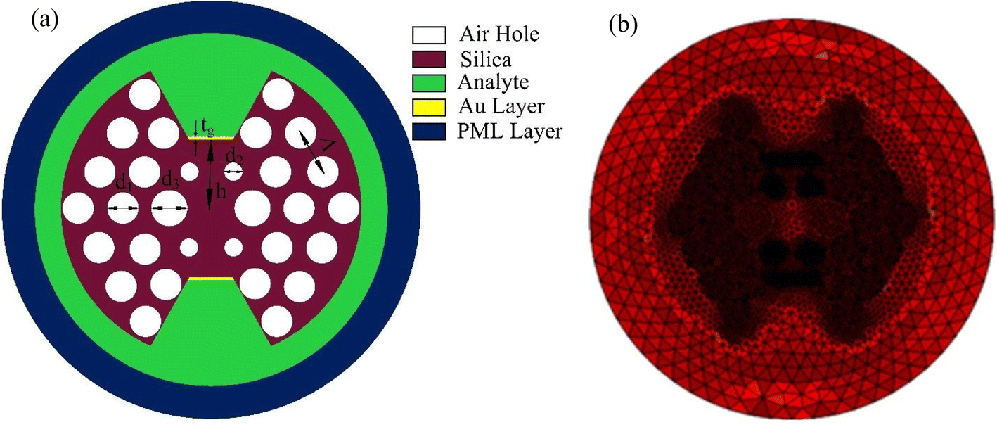 | ||
| Fig. 1 (a) Material and model structure. (b) 2D plot of the mesh structure. | ||
To simulate the sensor, we use the COMSOL Multiphysics software. The model analysis utilizes triangular-shaped mesh elements. The proposed sensor mesh area is 7498 μm2, with an element area ratio of 3.264 × 10⁻⁵Table 1. The average element quality is 0.9552, and the minimum element quality is 0.7437. For the sensor analysis, the total number of triangular elements is 24848, with 1864 edge elements and 150 vertex elements. The mesh is depicted in Fig. 1(b).
| d 1 | d 2 | d 3 | h | t g | Λ |
|---|---|---|---|---|---|
| 0.65Λ | 0.34Λ | 0.85Λ | 1.6Λ | 30 nm | 9 μm |
It is crucial to accurately specify the material properties when simulating the sensor in COMSOL. In our case, we are using mode analysis for a PCF-based SPR sensor, so the refractive index specification of the material is very important. The refractive index for air holes has a real part of 1 and an imaginary part of 0. However, the refractive index for the analyte varies depending on the specific analyte. For this particular sensor, we are varying the refractive index of the analyte from 1.32 to 1.44. To specify the RI of gold we have to use the Drude–Lorentz equation7
 | (1) |
In the equation Δε is the weighting factor, ε∞ is the permittivity, ω is the angular frequency, ωD/2π is the plasma frequency, γD/2π is the damping frequency, ΩL/2π is the Lorentz oscillators frequency and ΓL/2π is the spectral width.
To specify the material properties of silica Sellmeier equation12 is necessary. From the equation we can calculate RI real and imaginary parts of silica.
 | (2) |
In order to practically implement of this sensor, a straightforward and cost-effective fabrication process is essential. To begin, a silica substrate is selected and thoroughly cleaned to ensure optimal performance. The design involves a hexagonal lattice structure with three layers of circular air holes, spaced at a pitch of 9 μm. This arrangement is transferred onto the substrate using a photolithography process.16 First, a photoresist layer is spin-coated, followed by UV exposure through a photomask that defines the lattice pattern. After development, the circular air holes are etched using reactive ion etching (RIE) or wet etching.17
For the bowtie-shaped channels, a deep reactive ion etching (DRIE) technique is applied to form these precise channels on the top and bottom of the sensor. These channels enhance the sensitivity of the sensor by improving the interaction between surface plasmon resonance (SPR) and the analyte.17–22 After patterning, a thin gold (Au) layer is deposited onto the surface of the sensor using thermal evaporation or sputtering, which supports the SPR effect.12 Finally, the sensor is cleaved and tested to ensure its performance in terms of refractive index detection.
Though variations in the fabrication dimensions may occur, such as ±1% or ±2% discrepancies in the air hole sizes and channel dimensions, studies show that these variations do not significantly affect the sensor's performance.3,12 The sensor remains highly sensitive and functional even with such variations, making it a flexible and reliable device for biosensing applications.
Result and discussions
The light from the core propagates along the gold surface at the resonant wavelength, as shown in Fig. 2(a). At this wavelength, maximum light absorption occurs in the gold layer, resulting in maximum loss. This is observed at the wavelength of 940 nm for an RI of 1.42, as shown in Fig. 2(c). Fig. 2(b) shows the SPP mode at the same wavelength. At the resonant wavelength (940 nm), the real part of the core mode light and the real part of the SPP mode light are matched, which is called the phase matching point, as illustrated in Fig. 2(c). In Fig. 2(c), the grey line represents the real part of the SPP mode obtained from the simulation, the orange line represents the real part of the core mode (x-polarized) also obtained from the simulation, and the blue curve represents the loss curve. The loss curve is calculated using eqn (3) based on the simulation results. From the simulation, we take the imaginary part of the effective mode of the x polarized core-guided mode and then use eqn (3) (ref. 14) to calculate the confinement loss.| α(dB cm−1) = 8.686 × k0Im(neff) × 104 | (3) |
 | (4) |
000 nm per RIU, which is significantly high. WLS is determined using eqn (5). Column 4 indicates the resolution of the sensor, with the maximum resolution achieved being 6.99 × 10⁻⁷ RIU, which is excellent for this type of sensor. Resolution is calculated using eqn (6).| Sλ (nm per RIU) = Δλpeak(na)/Δna | (5) |
| Rλ (RIU) = Δna × Δλmin/Δλpeak | (6) |
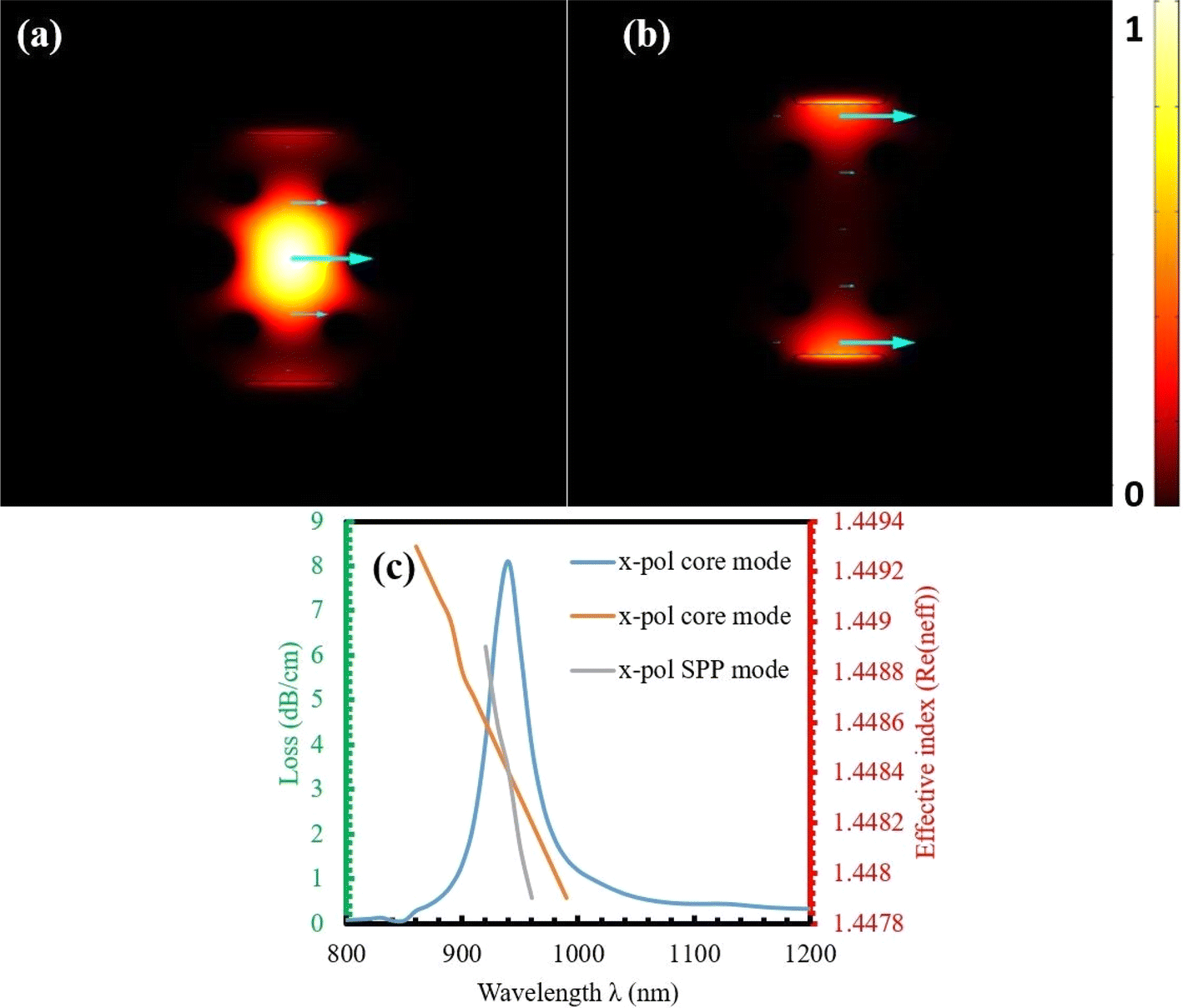 | ||
| Fig. 2 Electric field (EMW) distribution of x-polarize light at RI 1.42 (wavelength 940 nm). (a) Electric field (EMW) distribution of core mode at the resonant wavelength. (b) Electric field (EMW) distribution of SPP mode at the resonant wavelength. (c) Phase matching curve. | ||
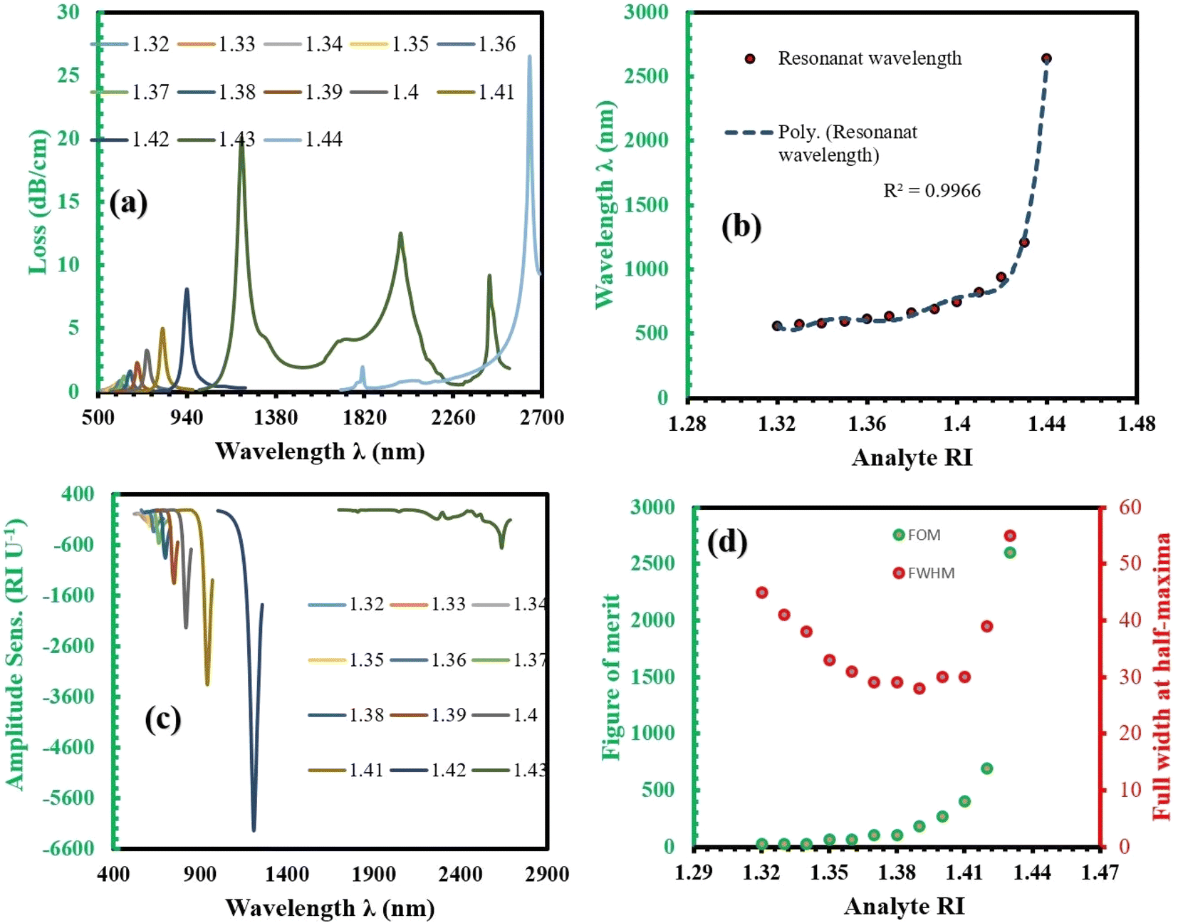 | ||
| Fig. 3 (a) EMW distribution curve for analyte RI range 1.32 to 1.44. (b) Polynomial fit curve for RI range 1.32 to 1.44. (c) Amplitude sensitivity for analyte RI 1.32 to 1.43 as a function of wavelength. (d) FOM and FWHM as a function of analyte RI. | ||
| RI | λ peak (nm) | S λ (nm per RIU) | R λ (RIU) | S A (RIU) | FWHM (nm) | FOM |
|---|---|---|---|---|---|---|
| 1.32 | 560 | 1000 | 1.00 × 10⁻⁴ | 82 | 45 | 22 |
| 1.33 | 570 | 1000 | 1.00 × 10⁻⁴ | 109 | 41 | 24 |
| 1.34 | 580 | 1000 | 1.00 × 10⁻⁴ | 156 | 38 | 26 |
| 1.35 | 590 | 2000 | 5.00 × 10⁻⁵ | 217 | 33 | 61 |
| 1.36 | 610 | 2000 | 5.00 × 10⁻⁵ | 323 | 31 | 65 |
| 1.37 | 630 | 3000 | 3.33 × 10⁻⁵ | 558 | 29 | 103 |
| 1.38 | 660 | 3000 | 3.33 × 10⁻⁵ | 851 | 29 | 103 |
| 1.39 | 690 | 5000 | 2.00 × 10⁻⁵ | 862 | 28 | 179 |
| 1.4 | 740 | 8000 | 1.25 × 10⁻⁵ | 2226 | 30 | 267 |
| 1.41 | 820 | 12000 |
8.33 × 10⁻⁶ | 3357 | 30 | 400 |
| 1.42 | 940 | 27000 |
7.70 × 10⁻⁶ | 6242 | 39 | 692 |
| 1.43 | 1210 | 143000 |
6.99 × 10⁻⁷ | 664 | 55 | 2600 |
| 1.44 | 2640 | NA | NA | NA | NA | NA |
In Table 2, we observe that our sensor can detect refractive indices (RIs) within the range of 1.32 to 1.44, which encompasses the RI values of several important biological and chemical analytes. This makes the sensor highly suitable for detecting a wide range of biological conditions, including cancerous cells, urinary disorders, and other biological fluids such as serum and blood. For example, normal human cells typically exhibit an RI range of 1.36–1.38,23–25 whereas cancerous cells (e.g., MDA-MB-231 breast cancer cells) have an RI between 1.38–1.42.23–25 Urine generally has an RI of 1.332–1.340,26,27 which varies depending on composition, while serum (a key component of blood) typically shows an RI of 1.34–1.36, and whole blood falls within the range of 1.36–1.40.26,28 Furthermore, common blood tests, which analyze biomarkers like glucose, proteins, and other disease indicators, also typically involve fluids with RIs within this detection range. The ability of our sensor to detect these RI values makes it an ideal tool for biomedical diagnostics, enabling sensitive and accurate detection of refractive index changes. This is crucial for real-time health monitoring, early disease detection, and environmental applications. The sensor's high sensitivity ensures reliable and precise results, highlighting its potential as a versatile biosensor for a wide range of applications.
Fig. 4 shows two important aspects of our PCF-based SPR sensors. In Fig. 4(a), we see the normal electric field distribution, which helps us understand how the electric field interacts with the analyte on the sensor surface. This is crucial for making our sensors more sensitive. Fig. 4(b) illustrates the Maxwell upward electric surface stress tensor, which is essential for analyzing the mechanical stresses at the sensor surface. This tensor helps us detect molecular changes with high accuracy, select specific analytes, and perform real-time analysis of molecular binding events. These capabilities make the Maxwell tensor a powerful tool for enhancing the performance and reliability of our sensors, ensuring precise and dependable results in various applications. The comprehensive analysis in Fig. 4 underscores the effectiveness of our PCF-based SPR sensors in delivering accurate and sensitive detection while maintaining structural integrity under mechanical stress.
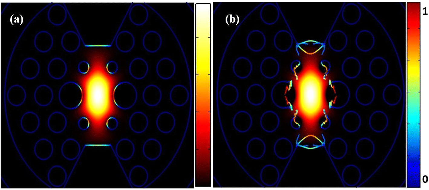 | ||
| Fig. 4 (a) Normal electric field distribution. (b) Maxwell upward electric surface stress tensor. | ||
The responsiveness of a sensor is greatly impacted by the thickness of the gold coating. The confinement loss and amplitude sensitivity across various thicknesses at refractive indices (RIs) of 1.34 and 1.35 are affected by the thickness of the gold layer is demonstrated in Fig. 5(a) and (b). Fig. 5(a) demonstrates that confinement loss increases as the gold layer thins from 30 to 20 nm, but the opposite trend is observed when reducing thickness from 40 to 30 nm. This indicates that the most significant interaction between the core mode and surface plasmon resonance (SPR) mode occurs with a 30 nm gold layer thickness, leading to the deepest penetration of the electric field. Moreover, a thicker gold layer shifts the phase-matching condition towards longer wavelengths. For instance, the loss peak shifts to progressively longer wavelengths from 590 nm, 620 nm, and 640 nm with increasing gold layer thicknesses respectively 20 nm, 30 nm, and 40 nm for an RI of 1.35. Consequently, the sensitivity to wavelength also changes from 71 per RIU, 156 per RIU, and 152 per RIU for the corresponding gold layer thicknesses of 20 nm, 30 nm and 40 nm. As illustrated in Fig. 5(b), the thickness of the gold layer also affects signal strength, reaching its peak at 30 nm for the chosen RIs. Therefore, based on these findings, a 30 nm gold layer thickness is selected for optimal sensor performance.
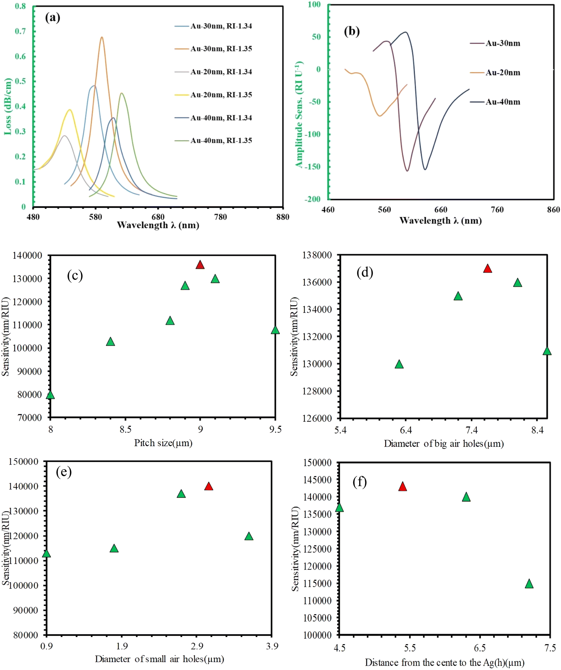 | ||
| Fig. 5 (a and b) Effect of gold layer thickness on confinement loss spectrum and amplitude sensitivity for varying gold thickness from 20 to 40 nm. (c–f) Optimization of pitch, diameter of big air hole, diameter of small air hole and distance from the center to the plasmonic layer. | ||
Fig. 5(c–f) illustrate the optimization process for the pitch, air hole diameter, and channel height of the sensor. First, we varied the pitch size and measured the wavelength sensitivity for each size (Fig. 5(c)). The sensor exhibited maximum wavelength sensitivity at a pitch of 9 μm, with sensitivities of 80000 nm per RIU, 103000 nm per RIU, 112000 nm per RIU, 127000 nm per RIU, 136000 nm per RIU, 130000 nm per RIU, and 108000 nm per RIU for pitch sizes of 8 μm, 8.4 μm, 8.8 μm, 8.9 μm, 9 μm, 9.1 μm, and 9.5 μm, respectively. Next, we optimized the diameter of the large air holes (Fig. 5(d)). The analyzed diameters were 6.3 μm, 7.2 μm, 7.65 μm, 8.1 μm, and 8.55 μm, yielding sensitivities of 130000 nm per RIU, 135000 nm per RIU, 137000 nm per RIU, 136000 nm per RIU, and 131000 nm per RIU, respectively. The optimal diameter was 7.65 μm, providing the highest sensitivity. We then analyzed the sensitivity for varying diameters of the small air holes (Fig. 5(e)). Diameters of 0.9 μm, 1.8 μm, 2.7 μm, 3.06 μm, and 3.6 μm resulted in sensitivities of 113000 nm per RIU, 115000 nm per RIU, 137000 nm per RIU, 140000 nm per RIU, and 120000 nm per RIU, respectively. The maximum sensitivity was achieved with a small air hole diameter of 3.06 μm. Finally, we optimized the distance between the center and the plasmonic layer (Fig. 5(f)). Distances of 4.5 μm, 5.4 μm, 6.3 μm, and 7.2 μm resulted in sensitivities of 137000 nm per RIU, 143000 nm per RIU, 140000 nm per RIU, and 115000 nm per RIU, respectively. The optimal distance was determined to be 5.4 μm, providing the highest sensitivity. Through this optimization process, we achieved a maximum wavelength sensitivity of 143000 nm per RIU.
In Fig. 6, we analyze how noise affects the performance of the sensor, particularly focusing on the confinement loss (CL), measured in dB cm−1. Fig. 6(a) examines the change in CL as a function of the small air hole size for two refractive indices (RIs) of 1.34 and 1.35. For the normal case, the maximum losses are 0.4797 dB cm−1 for RI 1.34 and 0.6776 dB cm−1 for RI 1.35. When noise is introduced, the confinement loss increases: with −6% noise, the maximum loss rises to 0.6462 dB cm−1 for RI 1.34 and 0.9160 dB cm−1 for RI 1.35; at −12% noise, the losses further increase to 0.8375 dB cm−1 for RI 1.34 and 1.1903 dB cm−1 for RI 1.35; with +6% noise, the maximum loss decreases to 0.3630 dB cm−1 for RI 1.34 and 0.5111 dB cm−1 for RI 1.35; and with +12% noise, it decreases even further to 0.2324 dB cm−1 for RI 1.34 and 0.3254 dB cm−1 for RI 1.35. These changes represent a 35% increase at −6% noise, a 74% increase at −12% noise, a 24% decrease at +6% noise, and a 51% decrease at +12% noise compared to the normal case.
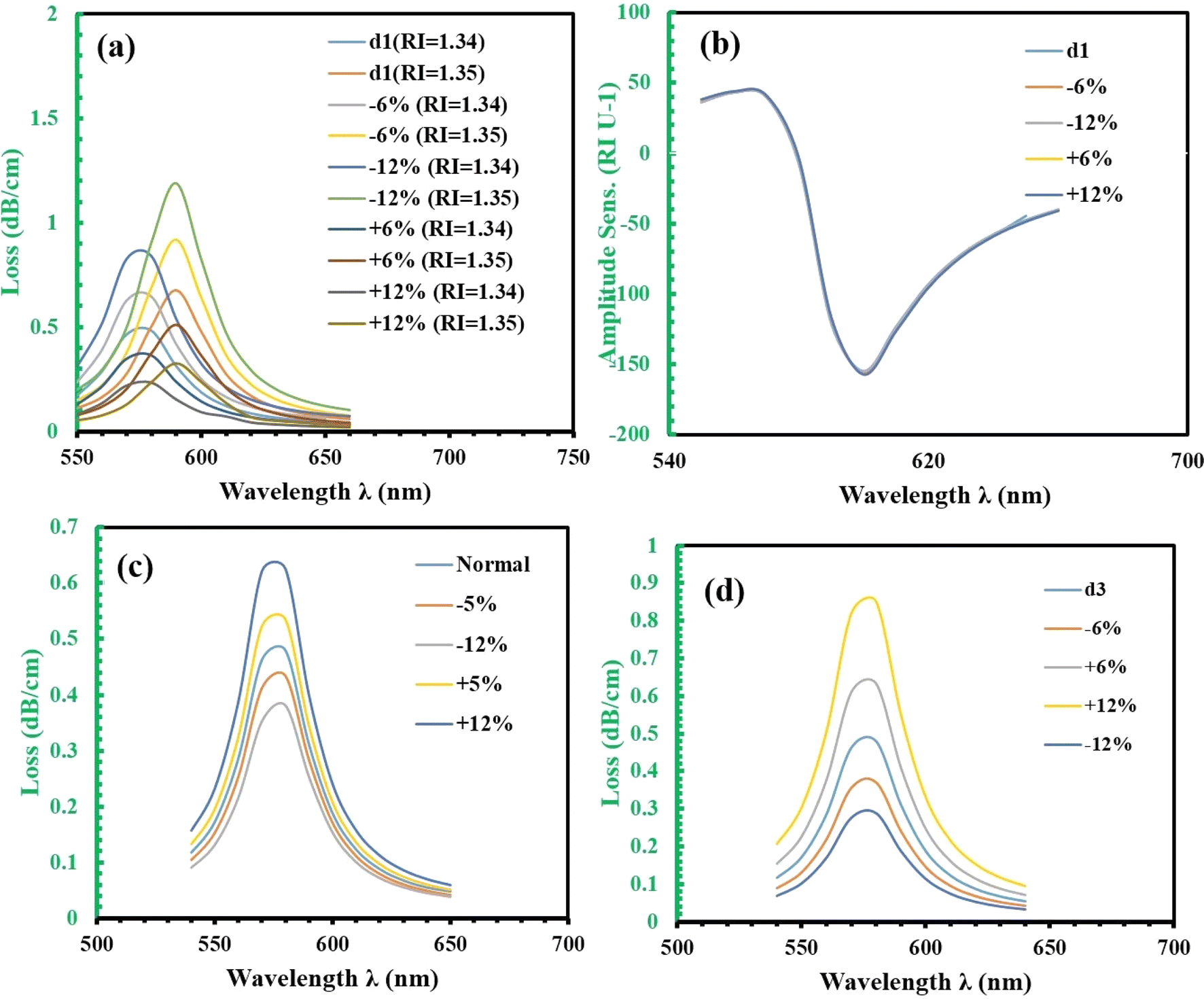 | ||
| Fig. 6 (a) Air hole size noise tolerance investigation on confinement loss of RI 1.34 and RI 1.35. (b) Noise tolerance investigation on amplitude sensitivity. (c) Position noise tolerance investigation on the RI 1.34 up to ±12%. (d) Noise tolerance on the big air hole up to ±12%. | ||
Fig. 6(b) shows that amplitude sensitivity (AS) remains largely unaffected by variations in the air hole size. Meanwhile, Fig. 6(c) focuses on the impact of position noise on the confinement loss. When position noise is applied to the small air hole, we observe significant variations in CL, with a 12% change in position leading to a 30% change in CL, while the resonant wavelength remains constant. For position noise at different levels, the maximum losses for RI 1.34 are: normal case 0.4797 dB cm−1, −5% noise 0.4334 dB cm−1, −12% noise 0.3813 dB cm−1, +5% noise 0.5343 dB cm−1, and +12% noise 0.6248 dB cm−1, representing a 9.7% decrease at −5% noise, a 20.5% decrease at −12% noise, an 11.4% increase at +5% noise, and a 30.3% increase at +12% noise compared to the normal case.
In Fig. 6(d), we investigate the influence of air hole diameter on the interaction between the light and the plasmonic material. As the diameter increases, more light interacts with the analyte, resulting in higher peak losses. Specifically, a 12% increase in the air hole diameter leads to a 70% increase in peak loss at the resonant wavelength compared to the optimal diameter. For the large air hole case at RI 1.34, the maximum losses at various noise levels are: normal case 0.4797 dB cm−1, −6% noise 0.3687 dB cm−1, −12% noise 0.6336 dB cm−1, +6% noise 0.8505 dB cm−1, and +12% noise 0.2887 dB cm−1, indicating a 23.2% decrease at −6% noise, a 32% increase at −12% noise, a 77% increase at +6% noise, and a 39.9% decrease at +12% noise compared to the normal case. Notably, these changes in diameter do not affect the wavelength sensitivity, emphasizing the sensor's robustness in terms of its wavelength response despite variations in structural parameters.
The Fig. 7 explores the effects of pitch and channel height (CH) on the confinement loss (CL) in a photonic crystal fiber (PCF) sensor, using RI 1.34 for analysis. Fig. 7(a) examines how pitch variations influence the confinement loss. In the normal case, the CL is 0.4797 dB cm−1, and it increases by 22.3% (0.5872 dB cm−1) under −3% noise. Under −6% noise, the CL decreases to 0.4154 dB cm−1, reflecting a 13.4% decrease. Meanwhile, for +3% noise, the CL is 0.4878 dB cm−1, showing a 1.7% increase, and under +6% noise, the CL drops to 0.4466 dB cm−1, indicating a 6.9% decrease. These results demonstrate that changes in pitch significantly affect the confinement loss, although the resonant wavelength remains unaffected.
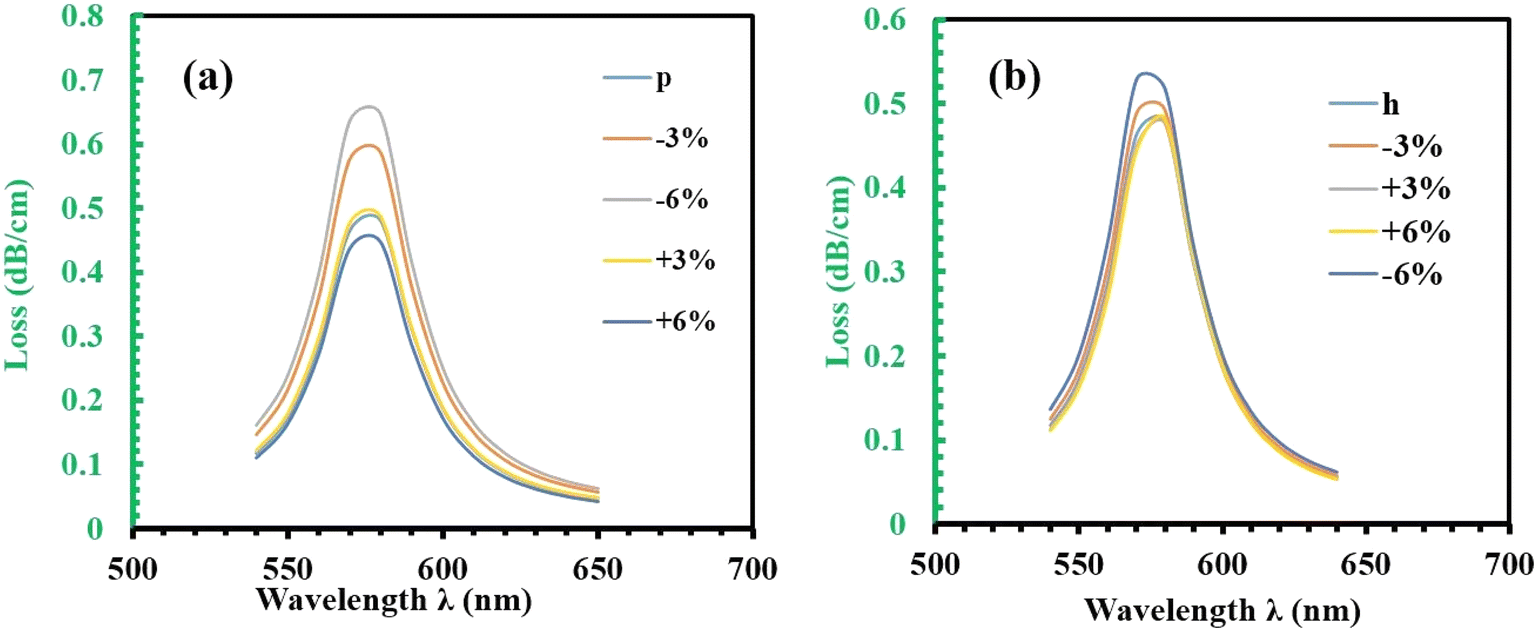 | ||
| Fig. 7 (a) Pitch tolerance on the confinement loss of RI 1.34 with in ±6%. (b) Channel distance tolerance from center of the plasmonic layer. | ||
Following this, Fig. 7(b) discusses the influence of channel height (CH) on confinement loss. In the normal case, the CL is 0.4797 dB cm−1, and for −3% noise, it slightly increases to 0.4930 dB cm−1 (a 2.7% increase). For +3% noise, the CL decreases slightly to 0.4766 dB cm−1 (0.6% decrease), and for +6% noise, it increases to 0.4821 dB cm−1 (0.5% increase). However, under −6% noise, the CL rises significantly to 0.5289 dB cm−1, showing an 8.2% increase. These variations indicate that as the channel height decreases, the confinement loss increases due to the stronger evanescent field interacting with the metal layer. Despite this, the resonant wavelength remains stable even with noise variations up to ±6%, highlighting the sensor's robustness against such structural changes. Both pitch and channel height impact the confinement loss, with pitch causing more substantial variations. However, the stability of the resonant wavelength under different noise conditions reinforces the sensor's reliability for practical applications.
Discussion
Table 3 demonstrates the comparison of the proposed sensor with various models from the literature spanning 2016 to 2024. Our proposed model outperforms the referenced works in key performance metrics, including wavelength sensitivity (WS), amplitude sensitivity (AS), resolution, and figure of merit (FOM). Specifically, our sensor achieves a remarkable wavelength sensitivity of 143000 nm per RIU, which is significantly higher than the highest value reported (80500 nm per RIU) in the literature. In terms of amplitude sensitivity, our model reaches 6242 per RIU, surpassing other models substantially. The wavelength resolution of our sensor is 6.99 × 10⁻⁷ RIU, indicating an unprecedented level of precision. Additionally, the figure of merit (FOM) of our proposed sensor stands at 2600, far exceeding the FOM values of the compared sensors. The impressive performance metrics of our sensor suggest its potential for practical implementation using feasible manufacturing technologies. It is capable of accurately detecting a wide range of analytes, making it highly suitable for various biosensing applications. The proposed sensor not only excels in sensitivity, resolution, and FOM but also demonstrates the feasibility of manufacturing and implementation, making it a superior choice for bio sensing compared to the existing models in the literature.
| Structure | RI range | WS (nm per RIU) | AS (RIU) | Resolution (RIU) | FOM | Ref. |
|---|---|---|---|---|---|---|
| Copper-graphene-based PCF biosensor | 1.33–1.37 | 2000 | 140 | 5.0 × 10⁻⁵ | NA | 29 |
| Ultra-low loss SPR PCF | 1.34–1.37 | 8500 | 335 | 1.16 × 10⁻⁵ | NA | 10 |
| Highly sensitive gold coated SPR PCF | 1.35–1.41 | 14500 |
4738 | 6.9 × 10⁻⁶ | 387 | 13 |
| V-shape SPR sensor | 1.29–1.44 | 88000 |
3136 | 1.14 × 10⁻⁶ | 1517 | 7 |
| Dual cluster and dual array-based PCF-SPR biosensor | 1.32–1.43 | 80500 |
3807 | 1.24 × 10⁻⁶ | 2115 | 14 |
| Highly sensitive SPR PCF (gold coated) | 1.32–1.43 | 36500 |
5269 | 2.74 × 10⁻⁶ | 744 | 15 |
| (AZO coated) | 1.19–1.42 | 8500 | 3593 | 1.18 × 10⁻⁵ | 413 | 15 |
| Arc-shaped gold-coated PCF SPR | 1.32–1.37 | 14100 |
109 | 7.09 × 10⁻⁶ | NA | 30 |
| This work | 1.32–1.44 | 143000 |
6242 | 6.99 × 10⁻⁷ | 2600 |
Conclusion
In this study, we introduced an optimized bowtie-shaped photonic crystal fiber (PCF) based surface plasmon resonance (SPR) biosensor for detecting various analytes. The sensor demonstrated exceptional performance, showcasing high amplitude sensitivity, wavelength sensitivity, and figure of merit (FOM) while offering a broad detection range from a single sensor. Specifically, the sensor achieved a remarkable wavelength sensitivity of 143000 nm per RIU and an amplitude sensitivity of 6242 per RIU. The impressive FOM of 2600 and a resolution of 6.99 × 10⁻⁷ RIU further highlight its precision and effectiveness. In order to overcome fabrication challenges, we have introduced a fabrication tolerance of up to 12%. A heightened channel is used to simplify the deposition of gold. Future research could explore the integration of titanium dioxide (TiO2) with gold to potentially enhance the sensor's performance. This combination may offer improved sensitivity and stability, paving the way for advanced biosensing applications. Overall, our findings suggest that the proposed bowtie-shaped PCF-based SPR biosensor is a highly effective tool for detecting biological and chemical substances, with considerable potential for future improvements and applications.
Data availability
Data will be available if there is any request from reviewers or editors.Conflicts of interest
There are no conflicts to declare.Acknowledgements
This research was supported by Institute for AI and Beyond for the University of Tokyo, JST, CREST grant number JPMJCR22O2, Japan, AMED under grant number JP22zf0127006, JSPS KAKENHI grant number JP20H05651, JP22K18804, JP23H04099.References
- J. Homola, Present and future of surface plasmon resonance biosensors, Anal. Bioanal. Chem., 2003, 377, 528–539, DOI:10.1007/s00216-003-2101-0.
- A. Das, M. A. Huraiya, H. Tabata and S. G. Ramaraj, Ultra-Sensitive Refractive Index Detection with Gold-Coated PCF-Based SPR Sensor, Talanta Open, 2024, 22, 100384, DOI:10.1016/j.talo.2024.100384.
- T. Ahmed, F. Haider, R. A. Aoni and R. Ahmed, Highly sensitive U-shaped micro-channel photonic crystal fiber-based plasmonic biosensor, Plasmonics, 2021, 16(6), 2215–2223, DOI:10.1007/s11468-021-01477-8.
- R. C. Jorgenson and S. S. Yee, A fiber-optic chemical sensor based on surface plasmon resonance, Sens. Actuators, B, 1993, 12(3), 213–220, DOI:10.1016/0925-4005(93)80021-3.
- A. Hassani and M. Skorobogatiy, Design criteria for microstructured-optical-fiber-based surface-plasmon-resonance sensors, J. Opt. Soc. Am. B, 2007, 24(6), 1423–1429, DOI:10.1364/JOSAB.24.001423.
- S. Cheng, W. Li, H. Zhang, M. N. Akhtar, Z. Yi, Q. Zeng, C. Ma, T. Sun, P. Wu and S. Ahmad, High sensitivity five band tunable metamaterial absorption device based on block like Dirac semimetals, Opt. Commun., 2024, 569, 130816, DOI:10.1016/j.optcom.2024.130816.
- M. A. Huraiya, S. A. Razzak, H. Tabata and S. G. Ramaraj, New Approach for a Highly Sensitive V-Shaped SPR Biosensor for a Wide Range of Analyte RI Detection, J. Phys. Chem. C, 2024, 128(36), 15117–15123, DOI:10.1021/acs.jpcc.4c04425.
- A. Vial, A. S. Grimault, D. Macías, D. Barchiesi and M. L. De La Chapelle, Improved analytical fit of gold dispersion: application to the modeling of extinction spectra with a finite-difference time-domain method, Phys. Rev. B:Condens. Matter Mater. Phys., 2005, 71(8), 085416, DOI:10.1103/PhysRevB.71.085416.
- E. K. Akowuah, T. Gorman, H. Ademgil, S. Haxha, G. K. Robinson and J. V. Oliver, Numerical analysis of a photonic crystal fiber for biosensing applications, IEEE J. Quantum Electron., 2012, 48(11), 1403–1410, DOI:10.1109/JQE.2012.2213803.
- S. Asaduzzaman and K. Ahmed, Investigation of ultra-low loss surface plasmon resonance-based PCF for biosensing application, Results Phys., 2018, 11, 358–361, DOI:10.1016/j.rinp.2018.09.026.
- Y. Zhao, Z. Q. Deng and J. Li, Photonic crystal fiber based surface plasmon resonance chemical sensors, Sens. Actuators, B, 2014, 202, 557–567, DOI:10.1016/j.snb.2014.05.127.
- T. Ahmed, A. K. Paul, M. S. Anower and S. A. Razzak, Surface plasmon resonance biosensor based on hexagonal lattice dual-core photonic crystal fiber, Appl. Opt., 2019, 58(31), 8416–8422, DOI:10.1364/AO.58.008416.
- M. R. Islam, A. N. Iftekher, K. R. Hasan, M. J. Nayen, S. B. Islam, R. Islam, R. L. Khan, E. Moazzam and Z. Tasnim, Surface plasmon resonance based highly sensitive gold coated PCF biosensor, Appl. Phys. A:Mater. Sci. Process., 2021, 127, 1–2, DOI:10.1007/s00339-020-04162-5.
- M. R. Islam, K. R. Hasan, M. M. Khan, A. N. Iftekher, F. Mehjabin, M. J. Nayen, J. A. Chowdhury, S. B. Islam and M. Islam, Design of a dual cluster and dual array-based PCF-SPR biosensor with ultra-high WS and FOM, Plasmonics, 2022, 17(3), 1171–1182, DOI:10.1007/s11468-022-01612-z.
- M. R. Islam, M. M. Khan, A. J. Yeasir, F. Mehjabin, J. A. Mim, J. A. Chowdhury, T. A. Nahid and M. Islam, Design and analysis of a highly sensitive SPR based PCF biosensor with double step dual peak shift sensitivity, Heliyon, 2023, 9(8), e18782, DOI:10.1016/j.heliyon.2023.e18782 , https://www.cell.com/heliyon/fulltext/S2405-8440(23)05990-X.
- D. M. Chow, S. R. Sandoghchi and F. M. Adikan, Fabrication of photonic crystal fibers, In 2012 IEEE 3rd International Conference on Photonics, IEEE, 2012, pp. 227–230, DOI:10.1109/ICP.2012.6379830.
- K. Nielsen, D. Noordegraaf, T. Sørensen, A. Bjarklev and T. P. Hansen, Selective filling of photonic crystal fibres, J. Opt. A: Pure Appl. Opt., 2005, 7(8), L13, DOI:10.1088/1464-4258/7/8/L02.
- A. A. Rifat, R. Ahmed, A. K. Yetisen, H. Butt, A. Sabouri, G. A. Mahdiraji, S. H. Yun and F. M. Adikan, Photonic crystal fiber based plasmonic sensors, Sens. Actuators, B, 2017, 243, 311–325, DOI:10.1016/j.snb.2016.11.113.
- D. Pysz, I. Kujawa, R. Stępień, M. Klimczak, A. Filipkowski, M. Franczyk, L. Kociszewski, J. Buźniak, K. Haraśny and R. Buczyński, Stack and draw fabrication of soft glass microstructured fiber optics, Bull. Pol. Acad. Sci., 2014, 62(4), 667–682, DOI:10.2478/bpasts-2014-0073.
- P. S. Menon, N. A. Jamil, G. S. Mei, A. R. Zain, D. W. Hewak, C. C. Huang, M. A. Mohamed, B. Y. Majlis, R. K. Mishra, S. Raghavan and N. Bhat, Multilayer CVD-Graphene and MoS2 Ethanol Sensing and Characterization Using Kretschmann-Based SPR, IEEE J. Electron Devices Soc., 2020, 8, 1227–1235, DOI:10.1109/JEDS.2020.3022036.
- J. R. Creighton and P. Ho, Introduction to Chemical Vapor Deposition (CVD), ASM International, 2001, vol. 407 Search PubMed.
- J. Boehm, A. François, H. Ebendorff-Heidepriem and T. M. Monro, Chemical deposition of silver for the fabrication of surface plasmon microstructured optical fibre sensors, Plasmonics, 2011, 6, 133–136, DOI:10.1007/s11468-010-9178-z.
- V. Kumar, S. K. Raghuwanshi and S. Kumar, Detection of early-stage cancer in adrenal gland (PC12) cells using a prism-based SPR biosensor, in Plasmonics in Biology and Medicine XXI, SPIE, 2024, vol. 12860, pp. 16–22, DOI:10.1117/12.2691275.
- M. Abdelghaffar, Y. Gamal, W. Soliman, Y. Badr, M. F. Hameed and S. S. Obayya, Early cancer detection by plasmonic PCF sensor, In 2022 International Conference on Numerical Simulation of Optoelectronic Devices (NUSOD), IEEE, 2022, pp. 147–148, DOI:10.1109/NUSOD54938.2022.9894779.
- M. Abdelghaffar, Y. Gamal, R. A. El-Khoribi, W. Soliman, Y. Badr, M. F. Hameed and S. S. Obayya, Highly sensitive V-shaped SPR PCF biosensor for cancer detection, Opt. Quantum Electron., 2023, 55(5), 472, DOI:10.1007/s11082-023-04740-w.
- D. Rajeswari and A. A. Revathi, Highly sensitive SPR-based PCF bio sensor for plasma cell detection in human blood for the detection of early stage cancer, Optik, 2022, 258, 168897, DOI:10.1016/j.ijleo.2022.168897.
- P. Manickam and R. Senthil, Numerical investigation of side-polished SPR PCF sensor for urine analysis, Plasmonics, 2022, 17(5), 2023–2030, DOI:10.1007/s11468-022-01688-7.
- I. Danlard and E. K. Akowuah, Assaying with PCF-based SPR refractive index biosensors: From recent configurations to outstanding detection limits, Opt. Fiber Technol., 2020, 54, 102083, DOI:10.1016/j.yofte.2019.102083.
- A. A. Rifat, G. A. Mahdiraji, R. Ahmed, D. M. Chow, Y. M. Sua, Y. G. Shee and F. M. Adikan, Copper-graphene-based photonic crystal fiber plasmonic biosensor, IEEE Photonics J., 2015, 8(1), 1–8, DOI:10.1109/JPHOT.2015.2510632.
- G. Melwin and K. Senthilnathan, Modelling a simple arc shaped gold coated PCF-based SPR sensor, J. Opt., 2024, 53(1), 117–126, DOI:10.1007/s12596-023-01110-3.
| This journal is © The Royal Society of Chemistry 2025 |