DOI:
10.1039/D4NH00463A
(Communication)
Nanoscale Horiz., 2025,
10, 549-560
Electric field-assisted resonance frequency tuning in free standing nanomechanical devices for application in multistate switching using a phase change material†
Received
12th September 2024
, Accepted 21st October 2024
First published on 22nd October 2024
Abstract
VO2 possesses a unique property of solid-state phase transition near room temperature wherein it transforms from monoclinic (M1) to tetragonal phase (R) that alters its physical properties, such as resistivity, mechanical modulus, and lattice strain, at an ultrafast time scale known as MIT. Such a phenomenon offers a distinct advantage to use VO2 in switching applications using heat flux as a stimulus. However, such alteration in properties can also be triggered under an electric field (E), which is known as E-MIT. A nanomechanical resonator coated with VO2 recently received traction where the resonance behavior can be modulated by taking advantage of its phase transition. Herein, we demonstrate that by fabricating a microstring of 400 μm (L) × 5 μm (W) × 240 nm (t) of suspended SiNx coated with VO2, the frequency (fr) of the resonator can be modulated by applying an electric field. We show that at room temperature, the fr of the microstring can be either reduced (by 0.5% at 15 V mm−1) or enhanced (by 2.2% at 25 V mm−1) or can be varied in a cycle under E-field. Using theoretical models, we establish the simulated results and explain the processes behind it, which demonstrate excellent mechanical tuning properties of the VO2-based microstring resonator, making it an attractive and alternative option for highly efficient MEMS-based switches and neuromorphic devices.
New concepts
This work reports a route to unveil the multi-stable switching state of E-field induced mechanical modulation of VO2 coated nanomechanical microstring resonator. The microstring resonator vibrating at its resonating frequency (fr) can be altered by applying varied E-field. We observed that on the application of periodic square pulses of E-field, the nanomechanical device showed periodic variation in its resonance frequency. However, this periodic vibration can be excited to multiple stable states upon varying the amplitude of periodic E-field. The observation of such phenomena in terms of mechanical frequency by modulation of E-field is unique and finds direct application in switching devices illustrated in this work. This multiple stable states of vibrations at room temperature is mainly due to the incorporation of TiO2 as an interfacial beneath VO2 that brings down the metal–insulator transition temperature of VO2 from ideal 67 °C to room temperature (around 30–35 °C). A direct observation of this lowered transition temperature was revealed by a few experimental measurements, such as observing variation in resistance as a function of temperature, change in resonance frequency with the temperature and temperature dependent Raman spectroscopic measurements.
|
1. Introduction
Nanomechanical resonators have been a great area of interest in the scientific community because of their extensive diversity of applications, including gas sensing and olfactory detection,1–3 photon and IR detection, phase transition studies, energy harvesting,4 actuation,5,6 mechanical property determination,7 molecular manipulation,8 and information processing.9–11 Nanomechanical resonators have received significant attention recently after the incorporation of phase change materials into this technology.12 Phase change materials possess unique advantages in creating stress, strain and force gradient due to the alteration of their intrinsic properties (like elastic modulus, thermal expansion coefficient, and magnetic properties) owing to the external stimuli (electric field, magnetic field, thermal, and optical), which is the basis of actuating devices.13–15 In order to address this purpose, transition metal oxides (TMOs) have been exploited extensively in the recent past where phase transitions arise from electronic correlation, lattice distortion and magnetic ordering, which give rise to the nonlinear change in various physical properties.16,17 Vanadium dioxide (VO2) is one of the candidates in the family of TMOs that shows such nonlinear variations in its physical properties at 68 °C (ideally) due to the structural phase transition (SPT) from monoclinic (M1) to tetragonal (R) phase like martensite. In its monoclinic phase, VO2 is electrically insulating or semiconducting in nature and exhibits conducting nature in the tetragonal phase. This unique behavior of VO2 around room temperature (around 68 °C) offers extra advantages over other materials that exhibit similar nature either at a very high temperature (e.g.: NbO2 at 800 °C) or at a very low temperature (e.g.: Fe3O4 at −154 °C, V2O3 at −123 °C). Furthermore, such a transition is believed to occur at a very fast rate (ultrafast scale). However, it is difficult to track such fast transition as it is limited by various constraints, such as heat dissipation rate of the material (thermal conductivity and heat capacity of the material), geometry of the device and measurement difficulties, such as data acquisition rate of the measuring instrument. Nevertheless, such fast transition is an encouraging factor to explore VO2 for different applications requiring quick response time when subjected to external stimuli. This transition is reversible in nature and occurs because of its change in crystal symmetry due to the transformation from monoclinic (M1) insulating phase (space group P21/c) to rutile (R) metallic phase (space group P42/mnm).18 More precisely, the dimerization of alternating V atoms, which results in two different V–V bond lengths and tilting of these dimmers with respect to the c-axis causes the transition.19 Although the mechanism of the transition still remains elusive, with two possible scenarios: a lattice distortion driven (Peierls-like) or an electron correlation driven (Mott-like),20 recently it has been proposed that the transition happens due to the strong interaction of electrons and phonons and hence it is described as “Mott-assisted Peierls” mechanism.18
Despite the puzzling physics of VO2, it has been widely explored in a variety of technological applications such as thermal,21 optical,22–24 electronic25 and thermoelastic switches,26 smart windows,27 microbolometer,28 nonvolatile and programmable memory,29,30 memristors,31 and actuators.32 Most of these applications are explored by exploiting the electronic properties of VO2. For instance, variation of its electrical conductance by the thermal stimulus is key for smart windows,27 microbolometer33 and thermal switches applications.34 On the other hand, VO2 also changes its electrical conductance isothermally under a critical electric field (Ec), which is known to be electric field-assisted metal–insulator transition (E-MIT).19,35,36 This property has been widely explored in nonvolatile memory, memristors and neuromorphic devices.37 Although there are numerous reports on VO2-based devices taking advantage of the electrical conductance change, however, there are few reports on variation of mechanical responses when it undergoes a thermal cycle.38,39 Rúa et al. were the first to observe this phenomenon by measuring the bending of VO2 microcantilever,40 whereas McGee et al. and Bukheri et al. showed similar behavior by measuring frequency change with the function of temperature and optical illumination.38,40–42 Recently, such modulation of mechanical responses was also observed by photothermal actuation by Wang et al.43 However, there is no such report where mechanical modulation can be controlled isothermally by manipulating DC electric field, taking the advantage of E-MIT property of the VO2. In this work, we report modulation of mechanical frequency of a suspended VO2-coated microstring using DC electric-field. The suspended VO2 microstring was allowed to vibrate using a piezoelectric vibrator. We show that the resonance frequency of the microstring can be reduced from its original value by applying the electric field lower than the critical E-field (Ec) whereas it can be enhanced by applying higher than Ec. The theoretical studies using the finite element method (FEM) employing COMSOL were performed to verify the E-MIT behavior of the VO2-coated microstring, which closely matched the obtained experimental observations. We demonstrate that localized temperature difference across the microstring changes significantly because of the Joule heating. This change in temperature thus changes the resonance frequency of the micro-string. The MIT behavior of VO2 can be greatly tuned by controlling the tensile stress of the film. Larger tensile stress shifts the MIT towards higher temperature as well as higher Ec, whereas larger compressive stress opposes both. Therefore to achieve MIT at lower temperature titanium dioxide (TiO2) was used as a buffer layer at the interface, which facilitates compressive stress during the growth of VO2, leading Tc to be lowered.44
2. Experimental details
Nanomechanical devices (microstrings) were fabricated using a nanofabrication facility. First, boron-doped p-type 〈100〉 Si wafers (dia ∼ 4′′) were thermally oxidized via wet oxidation in a tube furnace (Tystar) of 1.5 μm thickness at 1050 °C, followed by deposition of 200 nm thick stoichiometric silicon nitride (SiNx) on top by low-pressure chemical vapor deposition (LPCVD). The film stress was found to be 1.2 GPa measured by a Flexus 2320 stress measurement tool. The wafers were diced into 12.5 mm × 12.5 mm square-shaped coupons. The wafers are called SiNx/SiO2/Si. The wafers were cleaned in piranha solution followed by cleaning in acetone, IPA and water before depositing TiO2 and VO2 using the pulsed laser deposition (PLD) technique (as shown in Fig. S1 ESI†). Both VO2 and TiO2 were deposited onto SiNx/SiO2/Si wafers by (PLD) from vanadium (99.9% purity, American Elements) and titanium metal (99.9%purity, Kurt J Lesker) targets in an oxygen environment. A KrF (λ = 248 nm) excimer laser (Coherent, GmbH) was directed at the rotating target with a laser fluence of 2.6 J cm−2 and a repetition rate of 10 Hz. The substrate, maintained at 600 °C for the duration of the deposition, was placed directly opposite to the target, 31 mm apart. Oxygen pressure was maintained at 10 mTorr for TiO2 and 50 mTorr for VO2 deposition. Initially, TiO2 was deposited for 15 min followed by 30 min annealing time before depositing VO2 for 15 min. Parameters for the VO2 deposition were fully optimized in our previous work.45 After deposition, the phase and crystallinity were determined using the Rigaku XRD Ultima IV instrument and the surface morphology was studied by Bruker Dimension Icon atomic force microscopy (AFM). To validate the presence of TiO2 and VO2 and measure their thicknesses, transmission electron microscopy (TEM) was performed using a T20 microscope (ThermoFisher TecnaiTM T20) equipped with a LaB6 filament operated at 200 kV. TEM foils of thickness less than 100 nm were prepared using focused ion beam (FIB) machining, followed by the liftoff. The Raman characteristics of TiO2 and VO2 were studied using a Raman Spectrometer (model WITec alpha300R). The fabrication of VO2/TiO2 microstring was carried out by various microfabrication processes, as shown in Fig. 1(a)–(i), which have been discussed in our recent work.46 Here, we would like to emphasize that for maximum yield of nanomechanical devices, the greatest challenges lie in the release of the micro-string by etching the sacrificial SiO2 layer while protecting the VO2/TiO2/SiNx layer above it. For this, the efficient process was to etch VO2, TiO2 and SiNxvia reactive ion etching (RIE) while protecting the device with a Cr hard mask. Here again, the optimum choice of etchant gas and etching rate was necessary to avoid undercut and excess material removal, which was optimized by us in our earlier works.46 The VHF etchant was used to remove the sacrificial layer and release the micro-string as it prevents stiction issues which are commonly observed while using BOE as an etchant, thus maximising the yield, which was found to be more than 90%.
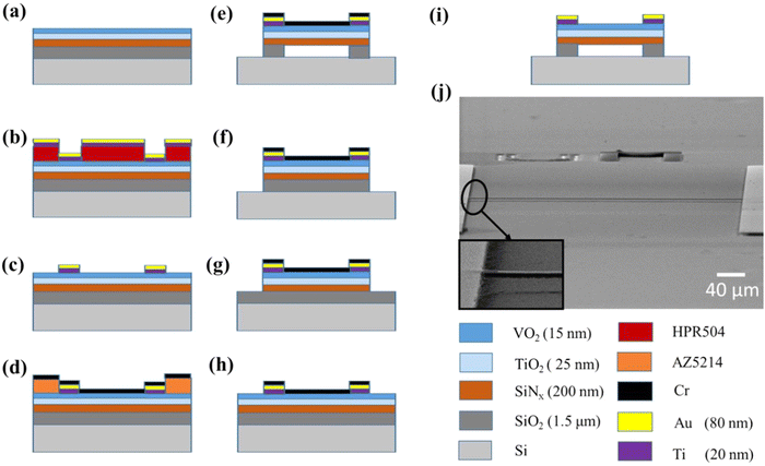 |
| | Fig. 1 Process flow to fabricate suspended nanomechanical resonator. (a) PLD-grown VO2/TiO2 on the starting substrate (SiNx/SiO2/Si). (b) HPR504 photoresist spin-coated to a thickness of about 1.3 μm, followed by patterning of contact pads by lithography and deposition of Au/Ti (80/20 nm) via sputtering. (c) Removal of resist in acetone to obtain contact pads. (d) Photoresist coating of AZ5214 by image reversal and lithography to deposit the Cr mask. (e) Stripping away photoresist by acetone through sonication. (f) RIE etching of VO2, TiO2 and SiNx through CHF3, CF4, and O2-based plasma. (g) Vertical removal SiO2. (h) Release of string by VHF etching of SiO2. (i) Removal of Cr mask by ICP to obtain the final microstring. (j) SEM image of the suspended nanomechanical device (micro-string). | |
All the microstrings were anchored to the contact pads of 3 mm × 3 mm dimensions coated with Au (80 nm)/Ti (20 nm) by E-beam evaporation. The dimension of the fabricated microstring resonator used in this study was 400 μm (L) × 3 μm (W) × 240 nm (t) as shown in the SEM image (Fig. 1(j)).
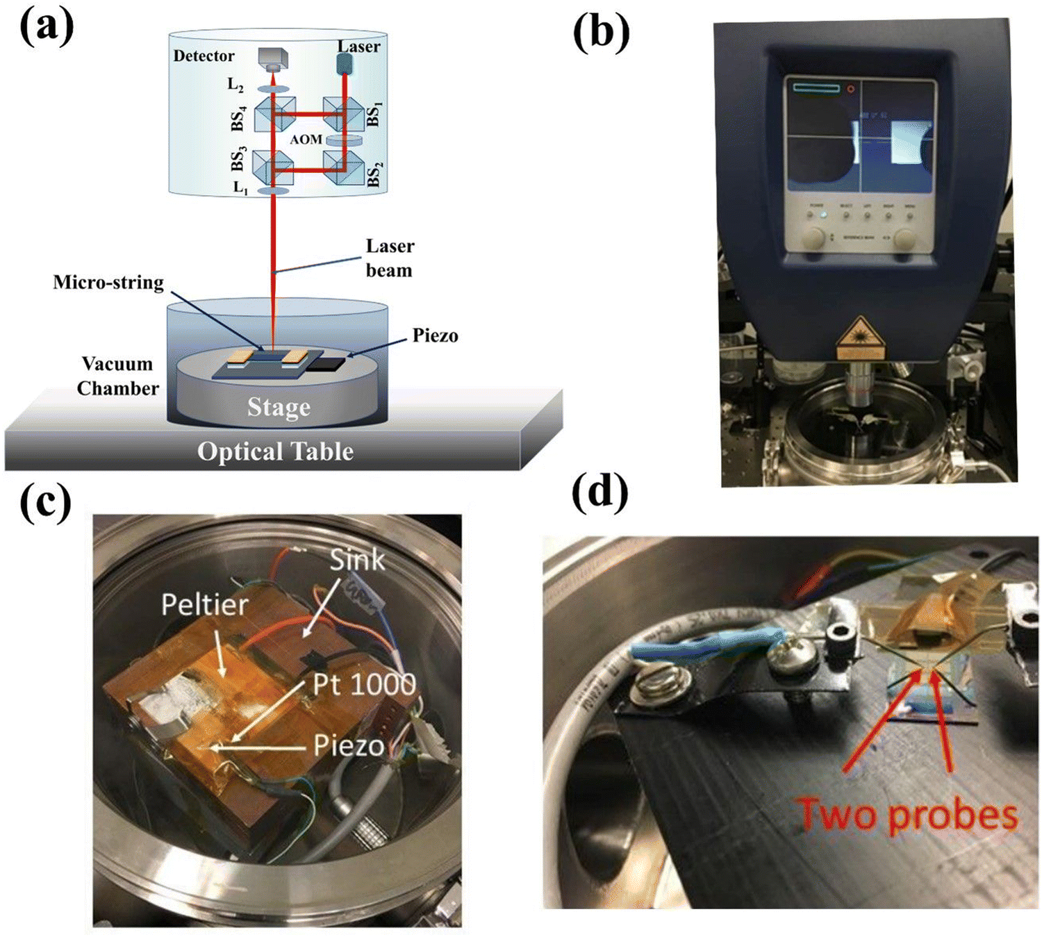
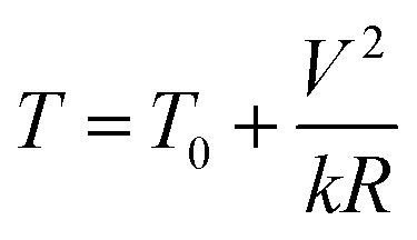
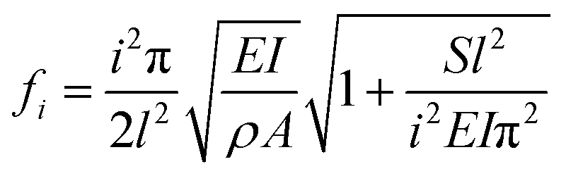
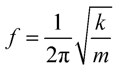
Furthermore, to investigate the electrical and mechanical behavior of microstring resonators, two independent measurements were carried out to probe MIT of VO2. In one case electrical resistance and I–V characteristics were performed with the function of temperature while in the other case, the resonance frequency of the device was measured again with the function of temperature. The former was performed by mounting the device on a probe station (Signatone) using a Keithley 2636 source meter by varying the temperature from 5 °C to 100 °C at an interval of 2 °C, equilibrating for 5 min in both the heating and cooling cycles. The latter, i.e. the measurement of resonance frequency, was carried out inside a vacuum chamber (at a pressure of 0.01 mTorr) using a laser Doppler vibrometer (LDV) (Polytech MSA500), as shown in Fig. 2(a) and (b). Furthermore, to study the E-field-dependent mechanical frequency of microstring, the experimental setup was modified using an in-house built additional attachment, where E-field was applied using electrical probes onto the contact pads. The two-probe setup was used to apply electric voltage across VO2 strings. Two aluminum sheets were bent in bracketed shapes and screwed on a PET (insulating) surface, which was screwed on a micro-manipulator. This would allow one to move the stage laterally and vertically. Spring-loaded pogo pins were glued at the unscrewed side of the brackets in such a way that they were fully compressed when they contacted the sample surface. Electrical connections were made via male–female adapters attached to the pogo pin-bracket set up via electrical feed, as shown in Fig. 2(c) and (d). The entire attachment along with the microstring device was kept inside the vacuum chamber wherein the device was rested on a peltier-driven heating stage. A piezo buzzer was mounted beside the device to facilitate the forced vibration to the microstring resonator.
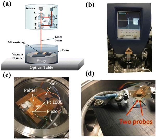 |
| | Fig. 2 (a) Schematic of LDV, (b) image of the LDV instrument, (c) integrated vacuum setup for electrical measurements, (d) zoomed electrical setup showing probe connections with contact pads of microstrings. | |
During the measurement, the temperature of the heater was swept from 20 °C to 100 °C at an interval of 2 °C equilibrating for 5 min in both the heating and cooling cycle. The controlled E-field was supplied via a BK Precision 9183 DC power supply with a computer-controlled software program. Dynamic mechanical response (frequency and amplitude) of the microstrings was recorded via LDV, at a pressure of 2.5 × 10⁻⁵ mbar as a function of the input electric field across the microstring via Au/Ti contact pads. A red laser (633 nm), built-in with LDV, with a minimum laser intensity of 22 μW was used to record the Doppler shift. The input voltage was ramped at 1 V min−1 (E-field ∼ 2.5 V mm−1 min−1) using a DC power supply. Further voltage pulses were toggled between 0 to +15 V, which corresponded to 0 and 37.5 V mm−1E-field across the microstring, to observe the mechanical response of the strings below and above the E-MIT.
3. Results and discussion
3.1 Experimental results
The structural characterizations of the prepared films before fabricating the device were carried out using XRD, which shows the formation of a polycrystalline VO2 (M1) phase along with a TiO2 rutile phase, as depicted in Fig. 3(a). Further identification of the TiO2 rutile phase and VO2 monoclinic phase was confirmed via Raman spectroscopy. Raman spectrum of the TiO2 film revealed its characteristic modes at 143 cm−1, 235 cm−1, 446 cm−1 and 611 cm−1 as shown in Fig. 3(b). After the deposition of VO2 on TiO2, the Raman spectra of TiO2/VO2 showed the presence of the TiO2-R phase, which overlaps with the monoclinic phase of VO2. This overlap is primarily attributed to the stretching and bending of V–O–V with peaks observed at 138 cm−1, 193 cm−1, 223 cm−1, 261 cm−1, 308 cm−1, 339 cm−1, 387 cm−1, 442 cm−1, and a characteristic peak at 613 cm−1, which has been reported in several articles,47 as shown in Fig. 3(b)-green spectra. Further temperature-dependent Raman study was performed to verify the presence of a monoclinic phase of the VO2. As temperature increases beyond the critical temperature (Tc), VO2 transforms from its monoclinic phase to its rutile phase and therefore all the characteristic vibrational modes associated with the VO2 monoclinic phase are suppressed, as shown in Fig. 3(c). Transformation of VO2 from the monoclinic phase to the tetragonal phase induces tensile stress between the layers of VO2 and TiO2 due to the lattice mismatch19 and therefore there is a mode shift in the characteristic peaks (143 cm−1 and 611 cm−1) of the TiO2 with 4.6 cm−1 and 6.34 cm−1, respectively, which is seen in the Raman spectrum beyond the critical temperature, as shown in Fig. 3(c). The shift in the Raman characteristic modes of the TiO2 is tabulated in Table 1.
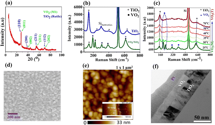 |
| | Fig. 3 (a) XRD of the VO2 and TiO2 films over microstring, (b) Raman peaks after TiO2 deposition and after VO2/TiO2 deposition over microstring, (c) temperature-dependent Raman spectra of VO2/TiO2 String from 25 °C to 70 °C, (d) surface morphology of the top-surface (VO2 deposited) and (e) AFM image of VO2/TiO2 deposited film with thickness of VO2/TiO2 grown film depicted in inset, (f) TEM image of the VO2/TiO2/SiNx film. | |
Table 1 Observed vibrational Raman modes of TiO2 with temperature and interface
| Temperature (°C) |
Raman mode (143 cm−1) |
Mode shift (Δω) |
Raman mode (611 cm−1) |
Shift (Δω) |
|
Phase |
| 25 |
145.6 |
2.6 |
615.86 |
4.86 |
Due to the initial interface of Si3N4 and VO2/TiO2 |
Stage-1 monoclinic |
| 30 ← Tc |
147.6 |
4.6 |
617.34 |
6.34 |
|
Stage-2 intermediate phase |
| 35 |
150.34 |
7.34 |
620.34 |
9.34 |
Increment in tensile stress due to phase transformation of VO2 from monoclinic to Rutile. |
|
| 40 |
150.34 |
7.34 |
620.34 |
9.34 |
|
Stage-3 rutile phase |
| 50 |
150.34 |
7.34 |
620.34 |
9.34 |
|
|
| 70 |
150.34 |
5.34 |
620.34 |
9.34 |
|
|
Furthermore, the surface morphology after the VO2 deposition was characterized by scanning electron microscopy (FESEM) and atomic force microscopy (AFM) as shown in Fig. 3(d) and (e). The surface roughness of the VO2 film was found to be around 4 nm and the morphology was found to be globular in nature, as shown in Fig. 3(e). The total thickness of the film was found to be 40 nm in which TiO2 and VO2 were 25 nm and 15 nm each, respectively, (Fig. 3(e) inset). The thickness of the individual films (TiO2 and VO2) was further verified by Transmission electron microscopy (TEM), as shown in Fig. 3(f).
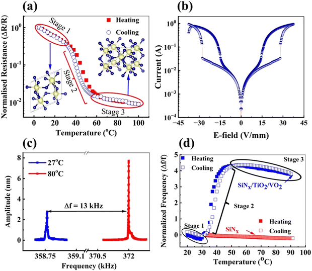
Once the primary characterization was performed, electrical measurements were collected on the fabricated microstring resonator, and it was observed that the electrical resistance of VO2-coated microstring reduces more than two orders of magnitude from its original value with the function of temperature when heated from 5 °C to 100 °C and recovers to the initial value in the cooling cycle with minimal hysteresis of 2 °C, as shown in Fig. 4(a). This large change in electrical resistance is due to the MIT of VO2, which occurs between 30 °C to 60 °C because of the structural transformation from the monoclinic (M1) to tetragonal (R) phase, which involves processes such as (Pierels-like) or electron–electron correlation (Mott-like) or both.48–50 This transition in electrical resistance predominantly occurs in three stages, as depicted in Fig. 4(a). Stage I is the semiconducting (or insulating phase), stage II is the intermediate phase and stage III is the metallic phase.
 |
| | Fig. 4 (a) Resistance changes of VO2 microstring as a function of temperature. (b) Current flow in VO2 microstring when an electric-field sweep is performed across it showing E-MIT at room temperature (30 °C). (c) Amplitude response and frequency response at room temperature and high temperature (d) normalized frequency change as a function of temperature of VO2-coated and bare (SiNx) microstrings. | |
The width of the hysteresis depends on the poly-crystalline nature of the VO2 film. Furthermore, it was also noticed in Fig. 4(b), that under bidirectional I–V sweep, the MIT occurred in the same device at an E-field of 27.5 V mm−1 at 30 °C. MIT under an electric field is often called electric field-dependent MIT (E-MIT). The magnitude of the electric field, to trigger MIT, reduces with increasing temperature. This is because the activation energy required for the transition under an electric field reduces as the device temperature increases.18 Increment in the temperature of the device on the application of a certain voltage across the terminal follows eqn (1)51
| |  | (1) |
Here, T0, k, V and R, are the ambient temperature, and thermal parameters (stiffness) that include heat capacities and thermal expansion coefficient, voltage applied across microstring and resistance of micro-string, respectively. The overall temperature of the device and applied E-field plays a crucial role in the phase transition of VO2.25,52 Due to the applied E-field, carrier concentration starts increasing, subsequently after critical E-field (Ec), a sudden increase in the carrier concentration occurs, which further accelerates the carriers under E-field leading to Joule heating and subsequently increase in the temperature, resulting in sudden increment of the current in the device, as shown in Fig. 4(b).25,51 Furthermore, an investigation of the mechanical response of the nanomechanical resonator was carried out using the laser Doppler vibrometer (LDV), and the data are shown in Fig. 4(c) and (d). The first order resonance frequency (fr) (fundamental mode) of the VO2/TiO2 deposited nanomechanical resonator was measured at 358.7 kHz at room temperature 27 °C with a quality factor (Q-factor) of 21,876. At a higher temperature of around 80 °C the fr of VO2/TiO2-coated microstrings increased by 3.7% from 358.7 kHz to 372 kHz, as shown in Fig. 4(c) with the reduction in Q-factor, which was found to be 13![[thin space (1/6-em)]](https://www.rsc.org/images/entities/char_2009.gif) 361. For a detailed analysis of the thermo-mechanical behaviour of the nanomechanical resonator, the variation of the normalized resonance frequency of the device as a function of temperature was examined and it was observed that for an uncoated resonator, the resonance frequency change showed a gradual decrease as expected because of the reduction in elastic modulus (as shown in Fig. 4(d)). However, for the VO2/TiO2-coated nanomechanical resonator, the fr decreases initially till 30 °C (can be considered as stage I) and then steeply increase up to around 50 °C (stage II), followed by gradual decrement beyond 50 °C (stage III), as depicted in Fig. 4(d). The observed phenomenon in Fig. 4(d) of the microstring resonator can be explained by the following expression mentioned in eqn (2).53
361. For a detailed analysis of the thermo-mechanical behaviour of the nanomechanical resonator, the variation of the normalized resonance frequency of the device as a function of temperature was examined and it was observed that for an uncoated resonator, the resonance frequency change showed a gradual decrease as expected because of the reduction in elastic modulus (as shown in Fig. 4(d)). However, for the VO2/TiO2-coated nanomechanical resonator, the fr decreases initially till 30 °C (can be considered as stage I) and then steeply increase up to around 50 °C (stage II), followed by gradual decrement beyond 50 °C (stage III), as depicted in Fig. 4(d). The observed phenomenon in Fig. 4(d) of the microstring resonator can be explained by the following expression mentioned in eqn (2).53
| |  | (2) |
where
i,
E,
ρ,
S,
A,
I and
l are the mode number of resonance frequency, elastic modulus, volume density, tensile stress, area, area moment of inertia and length of the microstring resonator, respectively. In general, the elastic modulus of any material decreases with increasing temperature,
54 which is given by the fundamental
eqn (3),
| |  | (3) |
where
k and
m are the stiffness and mass of the suspended microstring; there is a gradual decrease in the resonance frequency as was observed for the uncoated microstring resonator. For VO
2, it has been reported
55 that elastic modulus increases steeply at a temperature corresponding to the structural phase transition (SPT) region of VO
2. At the transition temperature range of VO
2, there is an increase in tensile stress due to lattice compression taking place in VO
2 because of its transformations from the monoclinic to the tetragonal phase,
42 this fact is also noticed in the Raman spectra of the VO
2/TiO
2 layers where vibrational modes shift as VO
2 transforms from the monoclinic phase to the rutile phase. Therefore, due to the increase in the tensile stress (
S) and elastic modulus of VO
2 in the transition temperature range, a sharp rise in its resonance frequency of 3.7% (stage II) is observed, which can also be evident from
eqn (2). However, in the region below and above the transition range (stage I and stage III), there is no structural transformation happening (VO
2 is in monoclinic and tetragonal in stage I and stage III, respectively) and the dynamic behaviour is completely controlled by the change in elastic modulus of VO
2 with temperature, thus resulting in gradual decrement of resonance frequency in these two regions. As depicted in
Fig. 4, the VO
2/TiO
2 coated resonator shows unusual behaviour with the variation in temperature as compared to the uncoated SiN
x/SiO
2/Si Microstring, which is solely assigned to the solid-state phase transition regardless of Mott-like or Peierls-like. The two observations, as shown in
Fig. 4(b) and (d), indicate that this phase transition can be triggered by an electric field, which can modulate the resonance frequency due to the change in the elastic modulus and the tensile stress. In other words, our hypothesis from the previous experiment is that electrical stimulus can modulate and control the mechanical stress or modulus in multiple directions. With the above motivation, we have demonstrated the modulation in the dynamics of the resonance frequency of the resonator by controlling the strength of the electric field, which is attributed to the EMIT phenomenon. Hence, to investigate the electro-mechanical response of the VO
2/TiO
2 microstrings, an electric field was applied across the resonator through pogo-pins attached to contact pads. The resonance behaviour of microstring was studied under an electric field applied in two different ways. In the first case, the
E-field was varied across the microstring in pulsating (on and off) manner, corresponding to which the resonance behaviour of strings was observed by measuring resonance frequency with the function of time. In the second case, the resonance frequency of the micro-strings was measured by varying
E-field in a linear ramping rate. In the first case, when the
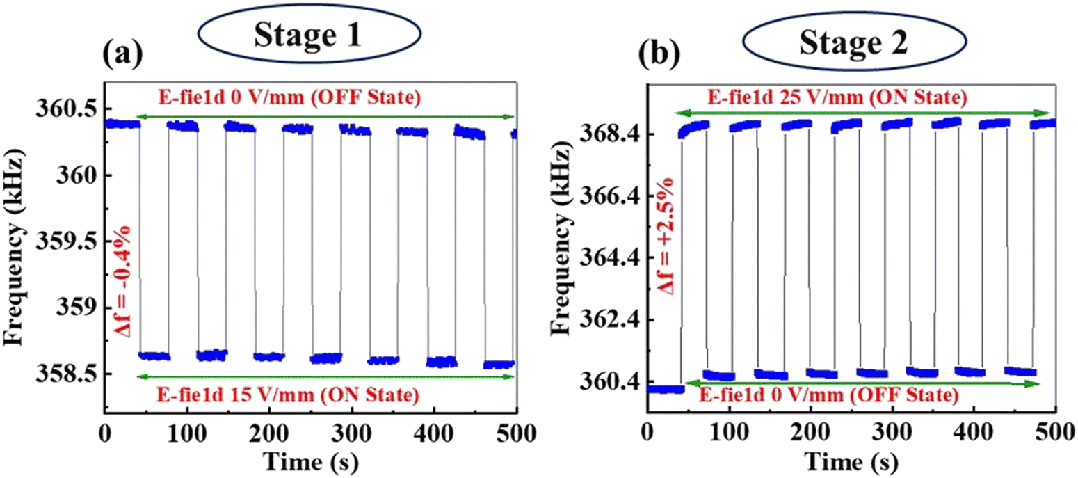
E-field was applied in a pulsating manner, the
fr of the resonator dropped by 0.5%, from 360.4 kHz to 358.6 kHz. This frequency remained stable at 358.6 kHz until the
E-field was turned off, at which point it returned to its original value of 360.4 kHz, as shown in
Fig. 5(a). However, when the higher
E-field (
i.e. 25 V mm
−1) was applied to the resonator in a similar pulsated manner, the resonance behaviour of the microstring just flipped and the corresponding resonance frequency of the resonator increased by 2.5% from 360.4 ± 0.3 kHz to 368.4 ± 0.3 kHz at the on state and dropped to its initial value
i.e. 360.4 ± 0.3 kHz at the off state as depicted in
Fig. 5(b).
 |
| | Fig. 5 Mechanical frequency modulation of the VO2/TiO2 microstring as a function of time (a) at 15 V mm−1 and (b) at 25 V mm−1 pulsating E-field. | |
To completely understand this resonance behaviour of microstrings due to the toggling of the E-field, the following approaches have been adopted. The experiment was performed in two different steps. In the first case, the E-field was toggled (on and off) from 0–15 V mm−1 to 0–32.5 V mm−1 in steps of 2.5 V mm−1. During this event, it was observed that the magnitude of the drop in resonance frequency (i.e., Δfr) of the resonator goes down till the E-field reaches 20 V mm−1. Beyond this value, increments in the resonance frequency of the resonator were observed up to 27.5 V mm−1. Further increment in the E-field (i.e. from 27.5 V mm−1 to 32.5 V mm−1), again resulted in the decrement of Δfr, as shown in Fig. 6(a). At higher E-field (≥20 V mm−1), as anticipated from the previous observation shown in Fig. 4(d), due to the localized heating of the microstring, the temperature reaches the range of phase transition temperature, which increases the elastic modulus and tensile stress of the resonator (as observed in stage-2 of Fig. 4(d)), resulting in a sharp increase in its resonance frequency. At a very high E-field (third stage, ≥27.5 V mm−1), once again the stiffness of VO2/TiO2 microstrings reduces and thus its frequency decreases. The switching speed (response time) of the device between the on and off states is very fast as the structural phase transition of VO2 is believed to be ultrafast as reported in several studies.56,57 Measuring such a fast response time is limited by the acquisition time of the measuring instrument. Therefore, we were not able to measure and quantify the exact response time of the mechanical frequency response of the microstring resonator. However, in our case, we believe that the response time of the VO2-coated resonator is majorly dependent upon the mechanical resonance frequency58 and the heat conductivity.59 The micro-string with a higher resonance frequency may possibly have a faster response time. In that case, one needs to play with the geometry of the string (length, width, and thickness) to increase the resonance frequency. Furthermore, heat-conducting and storing parameters such as thermal conductivity and specific heat capacity of the VO2 and the surrounding material decide the rate of the phase transition of VO2. It is desirable to have higher thermal conductivity for efficient phase transition and lower specific heat capacity for faster switching of transition from the insulator to metal and vice versa. In addition to this, the lower volume of VO2 material ensures faster dissipation of heat and hence enhances response time. The resonance behaviour of microstrings at two different linear rampings of the E-field in two different ranges of (0–27.5 V mm−1) and (0–37.5 V mm−1) were performed and data are shown in Fig. 6(b) and (c). It was observed that at the linear ramping of applied E-field from 0 to 27.5 V mm−1 with a ramping rate of 2.5 V mm−1 min−1, the frequency of VO2/TiO2 microstring resonator first decreases to 358.5 kHz till the E-field reaches 20 V mm−1 and subsequently increase to 370.5 kHz till the E-field reaches 27.5 V mm−1. While ramping down the E-field, the resonance frequency of the resonator drops down to 22.5 V mm−1 and then rises to the original state of resonance frequency (360.4 kHz) at 0 V mm−1. This resonance behaviour of microstrings during the ramping of the E-field undergoing trough and crest constitutes one cycle and follows the same periodic pattern when repeated ramping of the E-field was performed as shown in Fig. 6(b).
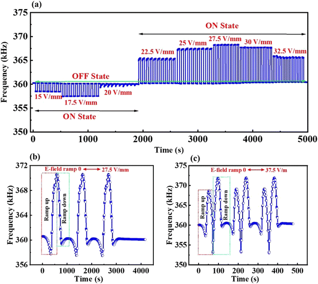 |
| | Fig. 6 (a) Frequency response of the VO2 microstring as a function of pulsating E-field from 15 V mm−1 to 32.5 V mm−1, (b) and (c) frequency responses of suspended VO2 microstring as a result of ramping E-field from 0–27.5 V mm−1 and 0–37.5 V mm−1. | |
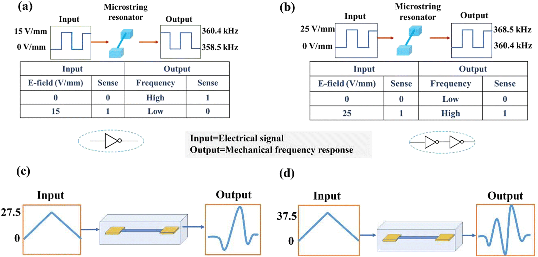
The periodic pattern in the resonance behaviour of VO2/TiO2 microstrings showed two peaks in one cycle when the E-field was varied from 0–37.5 V mm−1. This phenomenon can be explained from the obtained results of the resonance behaviour of microstrings during the toggling action of E-field as described earlier. The first peak is due to the increment of the E-field from 0 to 37.5 V mm−1 while the second peak is because of the reduction of the E-field from 37.5 V mm−1 to 0 V mm−1, as shown in Fig. 6(c). Careful observation delineates the reason for such unusual behaviour. From Fig. 6(a) it is clear that at a higher field than 27.5 V mm−1 the amplitude of the increment of frequency decreases, hence, when E-field was applied to the resonator from 0 to 37.5 V mm−1 it underwent a lowering of its frequency initially followed by a sharp increase in the fr. However, while decreasing the field from 37.5 V mm−1 to 0, it again undergoes critical values of E-field (i.e. 27.5 V mm−1), which shows a further increment in the frequency shift. The periodic pattern in the mechanical resonance frequency of the VO2-coated microstring is different from that of the periodic input E-field (shown in Fig. 6(c) and (d)). The possible explanation for this behaviour could be that ramping is performed in a continuous manner, which results in a faster rate of heat generation as compared to the rate of heat dissipation. Consequently, the output waveform varies compared to the input. The electromechanical response of the microstring resonator is promising. The immediate application that can be implemented by the obtained results is in the application of switching devices as the graph depicted in Fig. 5(a) and (b) can be modelled as the not gate and buffer gate as shown in Fig. 7(a) and (b), respectively. The micro-string modulated at a lower E-field or below MIT shows a drop in resonance frequency. If we consider 0 V mm−1 and 15 V mm−1 as high and low values, then the resonance frequency corresponding to 15 V mm−1 is reverse i.e., at lower E-field higher resonance frequency and at higher E-field lower frequency is the output from the resonator. Thus, it works like a NOT gate. At a higher E-field around 27.5 V mm−1, the behaviour is just reversed. In this case, 0 V mm−1 corresponds to lower frequency and higher E-field relates to higher resonance frequency, thus resembling the model of a double NOT gate or buffer gate. Similarly, the ramping response of the resonator can be implemented to obtain certain analogue behaviour, as shown in Fig. 7(c) and (d). Apart from this, pattern recognition applications can be modelled depending on the periodic frequency response of the VO2/TiO2-coated nanomechanical resonator on the application of the E-field applied in a periodically linear ramping manner. It is evident from the result that the periodic frequency response of the resonator is unique for two different linear ramping E-fields depending on the strength of the field. Therefore, one can store periodic frequency patterns corresponding to different ranges of linear ramped E-field as a reference signal and can compared to the frequency pattern generated from the test device to match the identity.
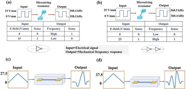 |
| | Fig. 7 Schematic sketch and truth table corresponding to (a) NOT gate, (b) buffer gate and frequency response pattern corresponding to the ramping signal from (c) 0 to 27.5 V mm−1, (d) 0 to 37.5 V mm−1. | |
3.2 Simulation results
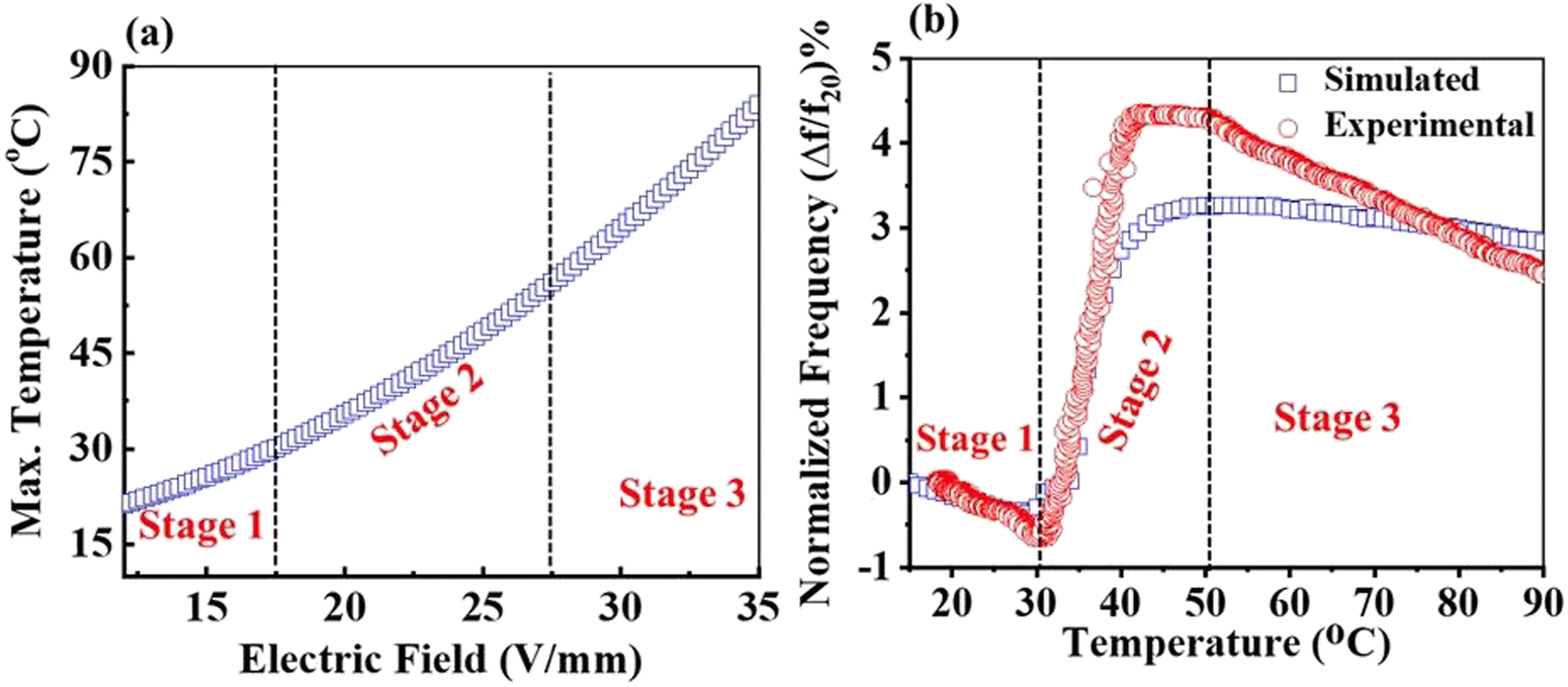
The simulation studies were carried out using FEM calculations to study and validate the obtained experimental results. The thermo-mechanical response of microstrings obtained using FEM studies is shown in Fig. 8. The simulated and the experimental result matches with good accuracy in the transition temperature region described in our work. However, there is a deviation in the obtained resonance frequency vs. the temperature curve in the simulation in comparison to the experimental result. We believe that this could be due to the fact that in reality there are many more factors such as defect and interfacial effects arising between TiO2 and VO2 that are difficult to incorporate into the simulation. The objective of the simulation was to observe the role of TiO2 in lowering the transition temperature range of VO2 and this has been accomplished by us. Here, we have designed the nanomechanical resonator as per the dimensions of the fabricated microstring. The VO2/TiO2 material was just added above it in the form of a uniformly distributed load (UDL). From the experimental data, combined Young's modulus values of VO2, TiO2 and SiNx were considered at different temperatures ranging from (20 to 100 °C). Further details of the entire simulation results are explained in the ESI† (S2 and S3). To understand the E-field induced MIT of VO2, FEM studies involving localised heating of the VO2 microstring on the application of DC-potential, were simulated. In this simulation, only VO2 and TiO2 layers were considered as SiNx is an insulating material and therefore current will only pass through the VO2/TiO2 layers. It is clear from the result as shown in Fig. 8(a) that application of a voltage across micro-string induces localised Joule heating effect and thus raise the temperature to an appreciable amount. At higher E-field or voltage localised temperature goes beyond MIT temperature. However, at lower E-field, it is well below the MIT temperature range. This result along with the thermo-mechanical simulation explains our experimental findings regarding the E-field-induced mechanical frequency switching behaviour of the VO2-based microstring resonator.
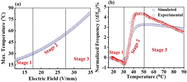 |
| | Fig. 8 (a) Maximum temperature across microstring due to applied electric field, (b) fundamental frequency variation of microstring as a function of temperature. | |
4. Conclusions
In summary, we report the fabrication of a VO2-coated suspended microstring resonator of length 400 μm along with TiO2 as an interfacial layer between the VO2 and SiNx layers. Structural characterization (XRD and Raman) showed that the deposited films are of polycrystalline nature and form the VO2 (M1) phase predominantly, the interfacial TiO2 layer forms as a rutile phase, which facilitates a lower stress thereby, reducing the phase transition temperature of VO2 from the M1 to R phase. Furthermore, we explored the mechanical modulation of the fabricated nanomechanical resonator by applying an electric field to the terminal points of the resonator and recording its dynamics by measuring the frequency of the device. Our observation was revealed by modulating the DC E-field, we are able to tune the mechanical frequency of the resonator in both directions (upward and downward) and the magnitude of the E-field can alter this mechanical modulation from 0.8 to 3.1%. We foresee that the resonance behaviour of VO2/TiO2 microstrings due to the toggling action of E-filed can be used as different states like what is observed in electronic switches and hence can be implemented in logic gate applications and consequently in the making of ultra-fast switching devices. Similarly, the periodic pattern in the resonance behaviour of microstrings on the application of different ramping E-field is unique and can be thought of utilizing this behaviour in the application of pattern recognition with some aid of machine learning algorithm. Therefore, the results obtained on the resonance behaviour of microstrings under two different modes of operation of the E-field have paved the way for ultrafast switching, logic gates and interesting neuromorphic applications.
Data availability
The data that support the findings of this study are available within the article and its ESI.†
Conflicts of interest
There are no conflicts to declare.
Acknowledgements
AG would also like to thank for SRG 2019/001984 from SERB, DST, FIST grant (SR/FST/ET-I/2020/628) from DST for the establishment of department Raman facility, SERB for the start-up grant, IIT Delhi for MFIRP (MI02442G) and SEED (PLN12/04MS) grant. The authors acknowledge the Department of Materials Science and Engineering (DMSE), Central Research Facility (CRF) and Nanoscale Research Facility (NRF) IIT Delhi and their staff, students and coordinators for helping and allowing to use of various characterization facilities. DB and JKA acknowledge the help from Mr Prashant Sharma from Semiconductor Device Fabrication Group, CSIR-CEERI, Pilani, India to operate the LDV. SAB would like to offer his gratitude to the facilities and staff of nanoFAB at the University of Alberta (U of A), Edmonton, Canada. AG and SAB acknowledge discussions with Prof. Thomas Thundat (Chemical and Biological Engineering SUNY, Buffalo) and for extending his support while he was at CME at U of A. Authors also offer their gratitude to the group members of the Advanced Electronic Materials and Systems (AEMS) Lab at IIT Delhi. HK and SKM acknowledge the TEM facility at AFMM, IISc Bangalore.
References
- E. Strelcov, Y. Lilach and A. Kolmakov, Nano Lett., 2009, 9(6), 2322–2326 CrossRef CAS PubMed.
-
J. Lu, T. Sagawa, L. Zhang, H. Takagi, D. F. Wang, T. Itoh and R. Maeda, presented at the The 8th Annual IEEE International Conference on Nano/Micro Engineered and Molecular Systems, 2013 (unpublished).
-
E. Bayraktar, D. Eroglu, A. T. Ciftlik and H. Kulah, presented at the 2011 IEEE 24th International Conference on Micro Electro Mechanical Systems, 2011 (unpublished).
- D. Shen, J.-H. Park, J. Ajitsaria, S.-Y. Choe, H. C. Wikle and D.-J. Kim, J. Micromech. Microeng., 2008, 18(5), 055017 CrossRef.
- A. S. Algamili, M. H. M. Khir, J. O. Dennis, A. Y. Ahmed, S. S. Alabsi, S. S. Ba Hashwan and M. M. Junaid, Nanoscale Res. Lett., 2021, 16(1), 16 CrossRef CAS.
- K. L. Ekinci, Small, 2005, 1(8–9), 786–797 CrossRef CAS PubMed.
- B. Xu, J. Zhu, F. Xiao, C. Jiao, Y. Liang, T. Wen, S. Wu, Z. Zhang, L. Lin, S. Pei, H. Jia, Y. Chen, Z. Ren, X. Wei, W. Huang, J. Xia and Z. Wang, Small, 2023, 19(24), 2300631 CrossRef CAS PubMed.
-
G. E. Fantner, P. D. Odermatt and H. A. Eskandarian, Springer Handbook of Nanotechnology, Springer, 2017, pp. 587–616 Search PubMed.
- F. C. Hoppensteadt and E. M. Izhikevich, IEEE Trans. Circuits Syst. I. Fundam. Theory Appl., 2001, 48(2), 133–138 CrossRef.
-
H. Yamaguchi and I. Mahboob, Foundations of Quantum Mechanics in the Light of New Technology, WORLD SCIENTIFIC, 2009, pp. 295–300 Search PubMed.
- S. Zhao, L. Li, C. Hu, B. Li, M. Liu, J. Zhu, T. Zhou, W. Shi and C. Zou, Adv. Sci., 2023, 10(21), 2300908 CrossRef CAS PubMed.
- A. Holsteen, I. S. Kim and L. J. Lauhon, Nano Lett., 2014, 14(4), 1898–1902 CrossRef CAS PubMed.
- M. Javanbakht, S. Mohebbi and H. Attariani, ACS Appl. Electron. Mater., 2023, 5(6), 3521–3530 CrossRef CAS.
- J. A. Kalb, Q. Guo, X. Zhang, Y. Li, C. Sow and C. V. Thompson, J. Microelectromech. Syst., 2008, 17(5), 1094–1103 Search PubMed.
- Y. Wang, J. Chai, S. Wang, L. Qi, Y. Yang, Y. Xu, H. Tanaka and Y. Wu, J. Appl. Phys., 2015, 117(6), 064502 CrossRef.
- A. G. Gavriliuk, I. A. Trojan and V. V. Struzhkin, Phys. Rev. Lett., 2012, 109(8), 086402 CrossRef PubMed.
- F. Wrobel, H. Shin, G. E. Sterbinsky, H.-W. Hsiao, J.-M. Zuo, P. Ganesh, J. T. Krogel, A. Benali, P. R. C. Kent, O. Heinonen and A. Bhattacharya, Phys. Rev. Mater., 2019, 3(11), 115003 CrossRef CAS.
- K. Liu, S. Lee, S. Yang, O. Delaire and J. Wu, Mater. Today, 2018, 21(8), 875–896 CrossRef CAS.
- U. Chitnis, S. Kumar, S. A. Bukhari, C. Soren, R.
K. Ghosh and A. Goswami, Appl. Surf. Sci., 2023, 637, 157916 CrossRef CAS.
- Z. Shao, X. Cao, H. Luo and P. Jin, NPG Asia Mater., 2018, 10(7), 581–605 CrossRef.
- A. Gupta, R. Aggarwal and J. Narayan, MRS Online Proc. Libr., 2009, 1174(1), 19–24 Search PubMed.
- M. Soltani, M. Chaker, E. Haddad, R. V. Kruzelecky and J. Margot, Appl. Phys. Lett., 2004, 85(11), 1958–1960 CrossRef CAS.
- M. Rini, Z. Hao, R. W. Schoenlein, C. Giannetti, F. Parmigiani, S. Fourmaux, J. C. Kieffer, A. Fujimori, M. Onoda, S. Wall and A. Cavalleri, Appl. Phys. Lett., 2008, 92(18), 181904 CrossRef.
- H. Lim, N. Stavrias, B. C. Johnson, R. E. Marvel, R. F. Haglund and J. C. McCallum, J. Appl. Phys., 2014, 115(9), 093107 CrossRef.
- G. Stefanovich, A. Pergament and D. Stefanovich, J. Phys.: Condens. Matter, 2000, 12(41), 8837–8845 CrossRef CAS.
- B. Viswanath, C. Ko and S. Ramanathan, Scr. Mater., 2011, 64(6), 490–493 CrossRef CAS.
- Y. Cui, Y. Ke, C. Liu, Z. Chen, N. Wang, L. Zhang, Y. Zhou, S. Wang, Y. Gao and Y. Long, Joule, 2018, 2(9), 1707–1746 CrossRef CAS.
- Q. Cheng, S. Paradis, T. Bui and M. Almasri, IEEE Sens. J., 2011, 11(1), 167–175 CAS.
- L. Pellegrino, N. Manca, T. Kanki, H. Tanaka, M. Biasotti, E. Bellingeri, A. S. Siri and D. Marré, Adv. Mater., 2012, 24(21), 2929–2934 CrossRef CAS PubMed.
- N. Manca, L. Pellegrino, T. Kanki, S. Yamasaki, H. Tanaka, A. S. Siri and D. Marré, Adv. Mater., 2013, 25(44), 6430–6435 CrossRef CAS PubMed.
- R. B. Naik, D. Verma and V. Balakrishnan, Appl. Phys. Lett., 2022, 120(6), 062101 CrossRef.
- N. Manca, L. Pellegrino, T. Kanki, W. J. Venstra, G. Mattoni, Y. Higuchi, H. Tanaka, A. D. Caviglia and D. Marré, Adv. Mater., 2017, 29(35), 1701618 CrossRef PubMed.
- C. Chen, X. Yi, X. Zhao and B. Xiong, Sens. Actuators, A, 2001, 90(3), 212–214 CrossRef CAS.
- H. Kim, K. Cheung, R. C. Y. Auyeung, D. E. Wilson, K. M. Charipar, A. Piqué and N. A. Charipar, Sci. Rep., 2019, 9(1), 11329 CrossRef PubMed.
- G. Gopalakrishnan, D. Ruzmetov and S. Ramanathan, J. Mater. Sci., 2009, 44(19), 5345–5353 CrossRef CAS.
- A. Pergament, P. Boriskov, N. Kuldin and A. Velichko, Phys. Status Solidi B, 2010, 247(9), 2213–2217 CrossRef CAS.
- S.-H. Bae, S. Lee, H. Koo, L. Lin, B. H. Jo, C. Park and Z. L. Wang, Adv. Mater., 2013, 25(36), 5098–5103 CrossRef CAS PubMed.
-
S. A. Bukhari, A. Goswami, R. McGee, R. Abraham, D. Hume, H. J. Chung and T. Thundat, presented at the 2020 IEEE 33rd International Conference on Micro Electro Mechanical Systems (MEMS), 2020 (unpublished).
- P. Parikh, C. Chakraborty, T. S. Abhilash, S. Sengupta, C. Cheng, J. Wu and M. M. Deshmukh, Nano Lett., 2013, 13(10), 4685–4689 CrossRef CAS PubMed.
- A. Rúa, F. E. Fernández and N. Sepúlveda, J. Appl. Phys., 2010, 107(7), 074506 CrossRef.
- R. McGee, A. Goswami, R. Abraham, S. Bukhari and T. Thundat, MRS Adv., 2018, 3(6–7), 359–364 CrossRef CAS.
- S. A. Bukhari, R. McGee, A. Mahdavi, F. Bensebaa, L. Zhou, H.-J. Chung, T. Thundat and A. Goswami, Adv. Electron. Mater., 2022, 8, 2100819 CrossRef CAS.
- T. Wang, D. Torres, F. E. Fernández, C. Wang and N. Sepúlveda, Sci. Adv., 2017, 3(4), e1602697 CrossRef PubMed.
- J. Li and J. Dho, J. Cryst. Growth, 2014, 404, 84–88 CrossRef CAS.
- R. McGee, A. Goswami, B. Khorshidi, K. McGuire, K. Schofield and T. Thundat, Acta Mater., 2017, 137, 12–21 CrossRef CAS.
- R. McGee, A. Goswami, S. A. M. Bukhari, L. Zhou, K. Shankar and T. Thundat, J. Microelectromech. Syst., 2019, 28(5), 766–775 CAS.
- M. Yang, Y. Yang, H. Bin, L. Wang, K. Hu, Y. Dong, H. Xu, H. Huang, J. Zhao, H. Chen, L. Song, H. Ju, J. Zhu, J. Bao, X. Li, Y. Gu, T. Yang, X. Gao, Z. Luo and C. Gao, Sci. Rep., 2016, 6(1), 23119 CrossRef CAS PubMed.
- N. F. Mott, Proc. Phys. Soc., London, Sect. A, 1949, 62(7), 416 CrossRef.
- J. B. Goodenough, J. Solid State Chem., 1971, 3(4), 490–500 CrossRef CAS.
- J. D. Budai, J. Hong, M. E. Manley, E. D. Specht, C. W. Li, J. Z. Tischler, D. L. Abernathy, A. H. Said, B. M. Leu, L. A. Boatner, R. J. McQueeney and O. Delaire, Nature, 2014, 515(7528), 535–539 CrossRef CAS PubMed.
- S. Rathi, J.-H. Park, I.-Y. Lee, J. M. Baik, K. S. Yi and G.-H. Kim, J. Phys. D: Appl. Phys., 2014, 47(29), 295101 CrossRef.
- A. Zimmers, L. Aigouy, M. Mortier, A. Sharoni, S. Wang, K. G. West, J. G. Ramirez and I. K. Schuller, Phys. Rev. Lett., 2013, 110(5), 056601 CrossRef CAS PubMed.
- S. S. Verbridge, J. M. Parpia, R. B. Reichenbach, L. M. Bellan and H. G. Craighead, J. Appl. Phys., 2006, 99(12), 124304 CrossRef.
- Y. Cai, K. Zhang, Z. Ye, C. Liu, K. Lu and L. Wang, Sensors, 2021, 21(12), 4242 CrossRef CAS PubMed.
- N. Sepúlveda, A. Rúa, R. Cabrera and F. Fernández, Appl. Phys. Lett., 2008, 92(19), 191913 CrossRef.
- A. S. Johnson, D. Perez-Salinas, K. M. Siddiqui, S. Kim, S. Choi, K. Volckaert, P. E. Majchrzak, S. Ulstrup, N. Agarwal, K. Hallman, R. F. Haglund, C. M. Günther, B. Pfau, S. Eisebitt, D. Backes, F. Maccherozzi, A. Fitzpatrick, S. S. Dhesi, P. Gargiani, M. Valvidares, N. Artrith, F. de Groot, H. Choi, D. Jang, A. Katoch, S. Kwon, S. H. Park, H. Kim and S. E. Wall, Nat. Phys., 2023, 19(2), 215–220 Search PubMed.
- K. A. Hallman, K. J. Miller, A. Baydin, S. M. Weiss and R. F. Haglund, Adv. Opti. Mater., 2021, 9(4), 2001721 Search PubMed.
- P. Sadeghi, A. Demir, L. G. Villanueva, H. Kähler and S. Schmid, Phys. Rev. B, 2020, 102(21), 214106 CrossRef CAS.
- Y. Zhou, S. Su, Z. Zhu, D. Hou, H. Zhang and Y. Cao, J. Appl. Phys., 2024, 136(13), 130901 CrossRef CAS.
Footnotes |
| † Electronic supplementary information (ESI) available. See DOI: https://doi.org/10.1039/d4nh00463a |
| ‡ Durgesh Banswar and Jay Krishna Anand contribute equally to this paper. |
|
| This journal is © The Royal Society of Chemistry 2025 |
Click here to see how this site uses Cookies. View our privacy policy here. 
 a,
Jay Krishna
Anand‡
a,
Jay Krishna
Anand‡