
Dipole-induced transitions from Schottky to Ohmic contact at Janus MoSiGeN4/metal interfaces†
Wen
Ai
 a,
Xiaohui
Hu
*ab,
Tao
Xu
c,
Jian
Yang
*ab and
Litao
Sun
c
a,
Xiaohui
Hu
*ab,
Tao
Xu
c,
Jian
Yang
*ab and
Litao
Sun
c
aCollege of Materials Science and Engineering, Nanjing Tech University, Nanjing 211816, China. E-mail: xiaohui.hu@njtech.edu.cn; yangjian1976@163.com
bJiangsu Collaborative Innovation Center for Advanced Inorganic Function Composites, Nanjing Tech University, Nanjing 211816, China
cSEU-FEI Nano-Pico Center, Key Laboratory of MEMS of Ministry of Education, Southeast University, Nanjing 210096, China
First published on 7th January 2025
Abstract
Janus MoSiGeN4 monolayers exhibit exceptional mechanical stability and high electron mobility, which make them a promising channel candidate for field-effect transistors (FETs). However, the high Schottky barrier at the contact interface would limit the carrier injection efficiency and degrade device performance. Herein, using density functional theory calculations and machine learning methods, we investigated the interfacial properties of the Janus MoSiGeN4 monolayer and metal electrode contacts. The results demonstrated that the n-type/p-type Schottky and n-type Ohmic contacts can be realized in metal/MoSiGeN4 by changing the built-in electric dipole orientation of MoSiGeN4. Specifically, the contact type of Cu/MoSiGeN4 (Au/MoSiGeN4) transfers from an n-type Schottky (p-type Schottky) contact to an n-type Ohmic (n-type Schottky) contact when the contact side of MoSiGeN4 switches from Si–N to Ge–N. In addition, the Fermi level pinning (FLP) effect of metal/MoSiGeN4 with the Si–N side is weaker than that of metal/MoSiGeN4 with the Ge–N side due to the effect of intrinsic dipole and interface dipole. Notably, a simplified mathematical expression ΔV/WM is developed to describe the Schottky barrier height at metal/MoSiGeN4 interfaces using the machine learning method. These findings offer valuable guidance for the design and development of high-performance Janus MoSiGeN4-based electronic devices.
New conceptsThe Janus MoSiGeN4 monolayer has gained significant attention due to its unique properties, including high electron mobility and mechanical stability, making it a promising candidate for nanoelectronic applications. However, the inevitable formation of a Schottky barrier between the MoSiGeN4 monolayer and the metal electrodes often limits charge injection efficiency. To address this challenge, we introduce a novel strategy to control the contact properties of metal/MoSiGeN4 interfaces by changing the built-in electric dipole orientation of MoSiGeN4. By switching the dipole's orientation, n-type Schottky, p-type Schottky, and n-type Ohmic contacts can be achieved. Notably, we developed a simplified mathematical expression, ΔV/WM, derived via machine learning, to predict the Schottky barrier height of metal/MoSiGeN4 interfaces with high accuracy. This study not only provides new insights into dipole engineering but also establishes a practical pathway for designing high-performance nanoelectronic devices based on Janus MoSiGeN4. |
Introduction
2D semiconductors have attracted tremendous attention as potential candidates in field-effect transistors (FETs) due to their unique atomic-scale thickness and lack of dangling bonds.1–8 In recent years, 2D semiconductor-based FETs have been extensively investigated, such as graphene,9,10 transition metal dichalcogenides (TMDs),11,12 and black phosphorene (BP).13,14 However, the absence of a bandgap in graphene impedes its effective modulation of current, rendering it unsuitable for traditional FET applications.15,16 Conversely, TMDs suffer from relatively low carrier mobility than silicon, which limits their potential in high-speed electronics.17,18 Additionally, BP-based FETs degrade rapidly in ambient air due to poor environmental stability.19,20 Therefore, selecting an appropriate 2D semiconductor with a suitable bandgap, excellent carrier mobility, and remarkable environmental stability is essential for the development of high-performance electronic devices.Recently, the successful synthesis of the MoSi2N4 monolayer has attracted enormous attention owing to its excellent carrier mobility and exceptional environmental stability,21,22 making it a promising candidate for next-generation FET applications. This breakthrough has led to increased research into MA2Z4 (M = Mo, W, V, Nb, Ta, Ti, Zr, Hf, or Cr, A = Si or Ge, Z = N, P, or As) materials,23–26 known for their exceptional properties in electronics. Among them, the Janus MoSiGeN4 monolayer stands out due to its novel asymmetric structure, disrupting mirror symmetry and introducing an inherent dipole moment. This configuration leads to novel properties such as tunable bandgap structures and spontaneous polarization effects,27–30 making the Janus MoSiGeN4 monolayer highly desirable for advanced electronic applications. Previous studies have reported that the Janus MoSiGeN4 monolayer exhibits excellent dynamical, thermal and mechanical stability, high experimental feasibility, and high electron mobility (∼5200 cm2 V−1 s−1),28,29 suggesting its potential applications in high-performance electronic devices.
In FETs, the performance is often impeded by the unavoidable Schottky barrier formed at the semiconductor–metal interface. The Schottky barrier height (SBH) depends on the difference between the work function of the metal and the electron affinity of the semiconductor, as well as the Fermi level pinning at the metal–semiconductor interface.31–35 Therefore, selecting an appropriate electrode material is essential to optimize the SBH and device performance. To improve the contact between the semiconductor and metal, various strategies have been employed to reduce the SBH, such as employing an external electric field,36–39 phase engineering,40 surface engineering,41 inserting a buffer layer,42,43 and using 2D metals as electrodes.44–49 For instance, a recent study demonstrated that the efficient modulation of SBH and Ohmic contacts can be achieved in MoSi2N4/M3C2 (M = Zn, Cd, Hg) contacts by applying a perpendicular electric field.37 It is found that O- and OH-modified Mo2B can form Ohmic contacts with WSi2N4, demonstrating surface-engineered Mo2B as a promising electrode for high-performance WSi2N4-based devices.41 The SBH and contact resistance were significantly reduced by inserting an ultrathin layer hexagonal boron nitride (h-BN) between the metal and MoS2, which enhanced the field effect mobility and output current in MoS2-based FETs.42 Our previous works indicated that the wide-range tunable SBH can be realized in CrI3 (CrBr3) and MoSi2N4 (WSi2N4) monolayers when in contact with 2D metal electrodes.44,45 However, their practical applications still have some limitations. The external electric field, phase engineering, and surface engineering are very challenging in practical applications. Inserting a buffer layer or using 2D metals as electrodes will increase tunneling resistance and influence the performance of the device. Therefore, selecting suitable channel materials and bulk metal electrodes is essential for improving electronic device performance.
In this work, the interfacial characteristics of the Janus MoSiGeN4 monolayer in contact with various metal electrodes (Al, Ag, Cu, Au, Pd, and Pt) are systematically investigated using DFT calculations. It is found that n-type Schottky, p-type Schottky, and n-type Ohmic contacts can be realized at metal/MoSiGeN4 interfaces by switching the built-in electric dipole orientation of MoSiGeN4. Among them, the transition from an n-type Schottky contact to an n-type Ohmic contact for Cu/MoSiGeN4 is observed when the contact side of MoSiGeN4 changes from Si–N to Ge–N. In particular, the effect between the intrinsic dipole and the interface dipole at metal/MoSiGeN4 interfaces leads to a weaker FLP effect on the Ge–N side than that of the Si–N side, resulting in a tunable Schottky barrier at metal/MGSN interfaces. Furthermore, Pd/MoSiGeN4 interfaces exhibit low tunneling specific resistivity and a small Schottky barrier height, suggesting that the Pd metal electrode is the best candidate electrode for Janus MoSiGeN4-based electronic devices.
Methods
Our DFT calculations were implemented in the VASP package by using the projector-augmented wave (PAW) method.50–53 We used the generalized gradient approximation (GGA) with the Perdew–Burke–Ernzerhof (PBE) function to describe the exchange–correlation interactions.54 To ensure accurate DFT calculations, the cutoff energy was set to 500 eV and the Monkhorst–Pack k meshes of 11 × 11 × 1 were applied. Atomic geometry optimizations are terminated until the energy difference and the maximal residual force are less than 10−5 eV and 0.01 eV Å−1, respectively. The DFT-D3 method of Grimme was applied to correct the van der Waals (vdW) interactions.55 The vacuum height along the vertical orientation was set to 20 Å to avoid periodic interactions between the neighboring slabs. Dipole correction was taken into account in all calculations. The dynamic stability of the MoSiGeN4 monolayer was determined using the density-functional perturbation theory (DFPT) as implemented in the Phonopy code,56 employing a 4![[thin space (1/6-em)]](https://www.rsc.org/images/entities/char_2009.gif) × 4 × 1 supercell.
× 4 × 1 supercell.
Results and discussion
The structure of the MoSiGeN4 monolayer contains a MoN2 layer sandwiched between the N–Ge and Si–N layers, exhibiting the typical asymmetric Janus structure, as shown in Fig. 1(a). The relaxed lattice constant of the MoSiGeN4 monolayer is 2.96 Å, which is consistent with the previously reported values.28,30,57 The bond lengths of Si–N, Ge–N, and Mo–N and the layer thickness of MoSiGeN4 are larger than those of MoSi2N4 (see Table S1, ESI†), due to the low electronegativity and larger radius of the Ge atom. The band structure and partial density of states (PDOS) of the Janus MoSiGeN4 monolayer are shown in Fig. 1(b). It can be seen that the MoSiGeN4 monolayer has an indirect bandgap of 1.36 eV, consistent with the previous results.28,30 The PDOS demonstrates that the conduction band minimum (CBM) of MoSiGeN4 mainly comes from the Mo d-orbital, while the valence band maximum (VBM) of MoSiGeN4 is mainly composed of the Mo d-orbital and N p-orbital. The absence of negative frequencies at the Γ point indicates that the MoSiGeN4 monolayer is dynamically stable (Fig. 1(c)). These results agree well with the previous reports28,30,57 | ||
| Fig. 1 (a) Crystal structure, (b) band structure, PDOS, and (c) phonon dispersion of the Janus MoSiGeN4 monolayer. | ||
To construct the contact between MoSiGeN4 and 3D metal electrodes, six bulk metals (Al, Ag, Cu, Au, Pd, and Pt) with the work function varying from 4.06 to 5.76 eV were used as metal electrodes of MoSiGeN4 (see Table 1). We take into consideration two different stacking configurations due to the asymmetry of Janus MoSiGeN4. For simplicity, the different built-in electric dipole orientations of MoSiGeN4 in contact with the metal electrodes are labeled metal/MSGN (Si–N side) and metal/MGSN (Ge–N side), as depicted in Fig. 2. Additionally, the metal/MoSiGeN4 interfaces in the following include both metal/MSGN and metal/MGSN interfaces. Given the electronic properties of MoSiGeN4 are obviously dependent on its lattice parameters,28 we strain the lattice constant of the metal to match the fixed lattice constant of the MoSiGeN4 monolayer. A six-layer metal atom configuration was employed to model the metal surface based on previous studies.58,59 We fixed the bottom two layers of the metal to emulate the metal substrates. The supercell matches are as follows, 1 × 1 MoSiGeN4 matches 1 × 1 Al (111), Ag (111), Au (111), Pd (111), and Pt (111) surfaces,  MoSiGeN4 matches the 2 × 2 Cu (111) surface. The calculated lattice mismatches range from 0.59% to 5.61%, as presented in Table S2 (ESI†).
| W M (eV) | d (Å) | E b (eV) | Φ N (eV) | Φ P (eV) | Φ N/P | |||
|---|---|---|---|---|---|---|---|---|
| Si–N | Ge–N | Si–N | Ge–N | Si–N/Ge–N | Si–N/Ge–N | Si–N/Ge–N | ||
| Al | 4.06 | 3.44 | 3.26 | −0.201 | −0.170 | 0.88/1.19 | 0.49/0.34 | p/p |
| Ag | 4.49 | 3.05 | 2.93 | −0.606 | −0.515 | 1.19/1.04 | 0.03/0.34 | p/p |
| Cu | 4.79 | 3.14 | 3.14 | −0.355 | −0.347 | 0.21/−0.02 | 1.27/1.47 | n/n |
| Au | 5.22 | 3.15 | 2.99 | −0.423 | −0.351 | 0.85/0.45 | 0.58/0.95 | p/n |
| Pd | 5.46 | 2.67 | 2.67 | −0.392 | −0.384 | 0.02/0.07 | 1.38/1.47 | n/n |
| Pt | 5.76 | 2.97 | 2.88 | −0.380 | −0.373 | 0.33/0.20 | 0.91/1.28 | n/n |
 | ||
| Fig. 2 Top and side views of (a) metal/MSGN and (b) metal/MGSN interfaces. | ||
The optimized geometrical structures of all metal/MoSiGeN4 interfaces are displayed in Fig. 2. The interlayer distance (d) between the metal and MoSiGeN4 is indicated in Fig. 2(a). We found that the interlayer distance of metal/MSGN interfaces ranges from 2.67 to 3.44 Å (2.67–3.26 Å for metal/MGSN interfaces), indicating a typical vdW interaction.47 To further evaluate the stability of the contact structures, the binding energy of the metal/MoSiGeN4 interfaces is calculated as follows:
| Eb = (EInterfaces − EMoSiGeN4 − EMetal)/N | (1) |
To further analyze the electron localization of metal/MoSiGeN4 interfaces, the electron location function (ELF) has been calculated, which can quantitatively evaluate the bonding behaviors.61,62 The ELF plots for metal/MSGN and metal/MGSN interfaces are depicted in Fig. 3(a) and (b). The ELF value quantitatively describes the localization of electron density, with a range from 0 to 1. The ELF value exceeding 0.5 indicates the presence of covalent bonds, while the value below 0.5 suggests the existence of ionic bonds or precursors to metallic bonds. The strength of a bond can be determined by its position within the ELF, particularly focusing on the saddle point, which is marked by the presence of two negative and one positive eigenvalue.47,63 The pentagram denotes the minimum ELF value situated at the midpoint of the curve, reflecting the bond point of metal/MoSiGeN4 interfaces (see Fig. 3(c) and (d)). We found that the minimum ELF values in metal/MSGN and metal/MGSN interfaces span from 0.039 to 0.058, as presented in Table S3 (ESI†). This observation suggests that the covalent bonding is absent in metal/MoSiGeN4. Such small ELF values demonstrate a weak interfacial interaction between metals and MoSiGeN4, which indicates that the interfacial interaction in metal/MoSiGeN4 interfaces is vdW interaction. Similar results can be found in 2D metals in contact with Janus MoSSe, such as germanene, VS2, NbS2, TaS2, and VSe2/MoSSe interfaces.47
 | ||
| Fig. 3 ELF plots for (a) metal/MSGN and (b) metal/MGSN interfaces. M–N bonds in (c) metal/MSGN and (d) metal/MGSN interfaces. The pentagrams denote the minimum ELE value located at the midpoint of the M–N bonds. | ||
The SBH is a crucial parameter for assessing the contact characteristics between semiconductors and metals. According to the Schottky–Mott rule,64 the value of the Schottky barrier height (ΦSB) is described as ΦN = EC − Ef for n-type SBH (ΦN) and ΦP = Ef − EV for p-type SBH (ΦP), where EC and EV represent the energy of the CBM, and VBM of the MoSiGeN4 monolayer, respectively. Ef is the Fermi level at the metal/MoSiGeN4 interfaces. Therefore, the SBH can be obtained from the projected band structures of MoSiGeN4 in metal/MoSiGeN4 interfaces, as summarized in Table 1 and Fig. 4. We found that the band structure of MoSiGeN4 is well preserved in all these metal/MoSiGeN4 interfaces. This is because the outer Si–N (Ge–N) layer of MoSiGeN4 acts as a buffer layer at the contact interface, which can protect the semiconducting characteristics of MoSiGeN4. The PDOS of MoSiGeN4 in all these metal/MoSiGeN4 interfaces shows that the VBM and CBM of MoSiGeN4 mainly originated from Mo d-orbitals and N p-orbitals, as shown in Fig. S1 and S2 (ESI†). These results suggest that the semiconducting characteristics are deeply embedded in the Mo–N layer, which makes the semiconducting characteristics protected by the outer Si–N (Ge–N) layer. A similar phenomenon has also been confirmed in metal contact with MoSi2N4, WSi2N4, CrC2N4, CrSi2N4, and Cs2PbI2Cl2.58,65,66
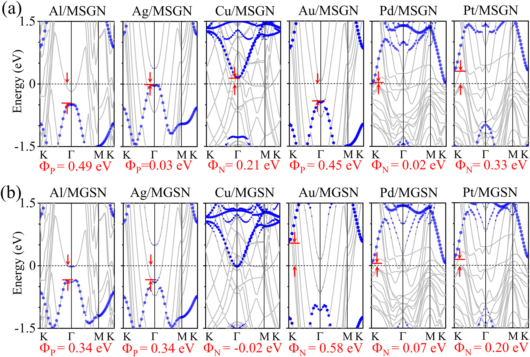 | ||
| Fig. 4 Projected band structures for (a) metal/MSGN and (b) metal/MGSN interfaces. The blue dots and gray lines represent contributions from MoSiGeN4 and the metal electrodes, respectively. The corresponding SBH values are listed at the bottom of the image. | ||
Next, the SBH values for metal/MoSiGeN4 interfaces are analyzed. For Au/MoSiGeN4 interfaces (see Fig. 4), the Fermi level shifts towards the VBM of MoSiGeN4 when Au contacts with the Si–N side, forming a p-type Schottky contact with ΦP = 0.45 eV. However, when Au contacts the Ge–N side, the Fermi level is closer to the CBM of MoSiGeN4, indicating an n-type Schottky contact with ΦN = 0.58 eV. For Cu metal, the transition from the n-type Schottky contact (ΦN = 0.21 eV) to the n-type Ohmic contact (ΦN = −0.02 eV) is observed when the contact side of MoSiGeN4 switches from Si–N to Ge–N. These results indicated that the contact types of Au/MoSiGeN4 and Cu/MoSiGeN4 interfaces can be efficiently adjusted by contacting Janus MoSiGeN4 with different sides. In addition, regardless of the contact side of MoSiGeN4, Al and Ag (Pd and Pt) form a p-type (n-type) Schottky contact. Specifically, the p-type SBH values of Ag/MSGN and Ag/MGSN interfaces are 0.03 and 0.34 eV, respectively. The ultralow p-type SBH for the Ag/MSGN interface (0.03 eV, see Fig. 4(b)) indicates the potential of Ag as an effective electrode for enhancing hole injection into the Janus MoSiGeN4 monolayer. While for Pd and Pt electrodes, the n-type SBH values of Pd/MSGN and Pd/MGSN interfaces are 0.02 and 0.07 eV, smaller than those of Pt/MSGN (0.33 eV) and Pt/MGSN (0.20 eV). It is found that Pd/MSGN and Pd/MGSN interfaces have ultralow n-type SBH (0.02 eV and 0.07 eV), suggesting the potential of Pd as the efficient electron injection electrode for the Janus MoSiGeN4 monolayer. Furthermore, we found that MoSiGeN4 tends to form p-type Schottky contacts in contact with metals of low work function, whereas it forms an n-type Schottky contact with metals of high work function, as summarized in Table 1.
The SBH exhibits significant sensitivity to the metal work function, as predicted by the Schottky–Mott rule.64 However, due to the strong FLP effect at the contact interface, the SBH becomes largely independent of the metal work function. To quantify the strength of the FLP effect, the pinning factor S is defined as follows,46,58,67
| S = |dΦN/P/dWM| | (2) |
 | ||
| Fig. 5 Schottky–Mott plot of (a) and (b) n-SBH and (c) and (d) p-SBH for metal/MSGN and metal/MGSN interfaces. | ||
The FLP effect in vdW contacts is primarily governed by the interface dipole (ΔD).33–35 The interface dipole at the metal/MoSiGeN4 interface induces a potential step (ΔV), resulting in a deviation of SBH from the ideal Schottky–Mott limit.30,47 Normally, the larger the potential step, the larger the Schottky barrier deviation. To reveal the origin of the Schottky barrier deviation, we obtain ΔV values by analyzing the differences in electrostatic potential energy between the two distinct sides of the metal/MoSiGeN4 interfaces. The ΔV value is calculated as ΔV = WC-Metal − WC-MoSiGeN4, where WC-MoSiGeN4 and WC-Metal represent the effective electrostatic potentials of MoSiGeN4 and metal side at metal/MoSiGeN4 interfaces. We corrected the Schottky–Mott plot by applying a ΔV correction, adding or subtracting ΔV to ΦN and ΦP. The corrected S values are SN = 0.95 and SP = 0.93 for metal/MGSN, and SN = 0.85 and SP = 0.89 for metal/MSGN (see Fig. S3, ESI†), respectively. These values are close to the Schottky–Mott limit, indicating that the ΔV value is the primary factor for the deviation of SBH from the ideal Schottky–Mott limit. Furthermore, we found a robust linear scaling relationship between the interface dipole (ΔD) and potential step (ΔV) for metal/MSGN and metal/MGSN, respectively, as illustrated in Fig. 6(a) and (b), consistent with the Helmholtz equation: ΔV = ΔD cosφ/εε0.73 To quantitatively evaluate the effect of the interface dipole on the FLP effect in metal/MoSiGeN4 interfaces, we calculated the plane-averaged differential charge density (Δρ) along the Z direction, where Δρ = ρInterfaces − ρMoSiGeN4 − ρMetal, with ρInterfaces, ρMoSiGeN4 and ρMetal representing the charge densities of the metal/MoSiGeN4 interface, isolated MoSiGeN4 monolayer, and isolated metal, respectively. We found that the Δρ values at the metal/MGSN interface are lower than those at the metal/MSGN interface (see Fig. S4, ESI†), demonstrating a weaker interface dipole for the metal/MGSN. This weaker dipole leads to a reduced FLP effect, as evidenced by higher S values for metal/MGSN (SN = 0.62 and SP = 0.64) compared to those of metal/MSGN (SN = 0.46 and SP = 0.43).
 | ||
| Fig. 6 The variation of ΔV with ΔD for (a) metal/MSGN and (b) metal/MGSN interfaces. The illustrations of dipole moment configurations in (c) metal/MSGN and (d) metal/MGSN interfaces. Specifically, the intrinsic dipole (D0), interface dipole (ΔD), and total dipole moment (Dtot) are depicted by red, blue, and black arrows, respectively. | ||
To further explore the effect of the interface diploe on ΔV, we investigate the total dipole moment Dtot = ΔD + D0, where Dtot is the total dipole moment of the metal/MoSiGeN4 interfaces, and D0 is the intrinsic dipole of the MoSiGeN4 monolayer (see Fig. S5, ESI†). The corresponding diploe moments are presented in Fig. 6(c) and (d). When metal contacts the Si–N side of MoSiGeN4, the ΔD and D0 values of Al, Ag, and Au/MSGN interfaces are in the same orientations, resulting in a larger Dtot (ranging from −0.219 to −0.418 e Å). For Cu, Pd, and Pt-MSGN interfaces, the smaller Dtot was obtained due to the opposite orientation of the ΔD and D0 values and the Dtot ranges from 0.007 e Å to 0.036 e Å. On the other hand, when the metal is in contact with the Ge–N side of MoSiGeN4, for the low work function metals (Al, Ag, Cu, and Au), the ΔD and D0 are in the opposite orientations, and their Dtot values are in the range of −0.025 to −0.230 e Å. While for the high work function metals (Pd and Pt), ΔD has the same orientation as D0, leading to a larger Dtot (0.028 and 0.055 e Å). In general, the total dipole moment (Dtot) of metal/MGSN interfaces is smaller than that of metal/MSGN interfaces, resulting in a weaker FLP effect and the S closer to the Schottky–Mott limit. Thus, the ΔV values can be enhanced (reduced) by the additive (offset) influence of interface dipole and intrinsic dipole, leading to the S deviating from (approaching) the Schottky–Mott limit. In addition, we also found a strong linear proportionality between ΔV and Dtot for metal/MoSiGeN4 interfaces, as shown in Fig. S6 (ESI†).
To gain a deeper understanding of the association between the SBH and various factors, we employed the machine learning model sure independence screening sparsifying operator (SISSO) to describe the mathematical relationships among these variables.74–76 We selected WM, Ef, ΔV, V0, Vint, Dtot, D0, ΔD, d, Eb, and Q as the feature descriptors, where V0 denotes the intrinsic potential step of the MoSiGeN4 monolayer, Q is the charge transferred from the metal to the MoSiGeN4 monolayer. The corresponding detailed data are provided in Table S4 (ESI†). To construct a huge feature space, the +, −, ×, /, exp, exp−,−1, 2, 3, 6, sqrt, cbrt, log, |−|, scd, sin, and cos were used as the mathematical operators., The seven different complexity descriptor cases were considered for obtaining the high-precision prediction results. The corresponding root mean square error (RMSE) of the SISSO model is displayed in Fig. 7(a) and (b). These results indicate that the RMSE for n-SBH ranges from 0.05 to 0.15, while for p-SBH, it ranges from 0.04 to 0.19. As the complexity of the descriptors increases, the RMSE decreases, leading to higher accuracy. Detailed information about the specific descriptors, R2, intercepts, and coefficients is shown in Table 2. It is evident that n-SBH and p-SBH exhibit strong correlations with ΔV and WM under different descriptor complexities. When the descriptor complexity is set to 1, the SISSO model gets the same descriptor for both n-SBH and p-SBH, namely, ΔV/WM. The specific mathematical expressions for n-SBH and p-SBH are given by 1.02 ΔV/WM + 2.01 and 0.4 ΔV/WM − 1.83, respectively, with corresponding R2 values of 0.9414 and 0.9384, as illustrated in Fig. 7(c) and (d). Thus, ΔV and WM are key factors in determining the SBH of the metal/MoSiGeN4 interfaces. Specifically, smaller ΔV and larger WM values can achieve n-type or p-type Ohmic contacts, which would improve the device performance based on metal/MoSiGeN4 interfaces.
 | ||
| Fig. 7 The variation of training RMSE with complexity for (a) n-SBH and (b) p-SBH. The values obtained by DFT calculations versus SISSO predictions for (c) n-SBH and (d) p-SBH. | ||
| Property | Descriptors | Complexity | R 2 | Intercepts | Coefficients |
|---|---|---|---|---|---|
| n-SBH | ΔV/WM | 1 | 0.9414 | 0.40 | −1.83 |
| ΔV/WM3 | 2 | 0.9567 | 0.34 | −40.72 | |
| abs((WM × Eb)(WM/Eb)) | 3 | 0.9680 | 0.03 | 0.16 | |
| W M/Eb × (sin(WM3)) | 4 | 0.9862 | 0.31 | −0.25 | |
| ΔV6/Eb × /(WM + ΔV)3 | 5 | 0.9900 | −0.29 | 0.00 | |
| abs(Ef × (WM − Ef) − exp(d) × (ΔV × VMSGN)) | 6 | 0.9922 | −0.07 | 0.06 | |
| ((WM − Vint) + (ΔV/Eb))/(Eb2 + sin(WM)) | 7 | 0.9927 | −0.32 | −0.09 | |
| p-SBH | ΔV/WM | 1 | 0.9384 | 1.02 | 2.01 |
| Q + (ΔV/WM) | 2 | 0.9570 | 0.97 | 2.20 | |
| Q + (ΔV/WM) | 3 | 0.9570 | 0.97 | 2.20 | |
| sqrt(exp(−ΔV))/sin(WM) | 4 | 0.9874 | 1.98 | 0.69 | |
| exp(sin(WM))/cbrt(exp(ΔV)) | 5 | 0.9919 | 2.55 | −3.31 | |
| cbrt(exp(−ΔV))/(d−1 − sin(WM)) | 6 | 0.9925 | 2.47 | −1.58 | |
| exp(D0)/log(d) − (scd(Vint) × sin(WM)) | 7 | 0.9964 | −1.95 | 2.88 |
Besides the Schottky barrier, the vdW gap introduces an additional tunneling barrier at the metal/MoSiGeN4 interface.77,78 This tunneling barrier also influences the efficiency of charge injection at the interface. The tunneling barrier can be obtained by the tunneling barrier height (ΦTB) and width (DTB). The ΦTB is determined by the effective potential difference between the vdW gap (Φgap) and the Fermi level (Ef),1,31,58 as illustrated in Fig. 8(a). The DTB value is also indicated in Fig. 8(a). The obtained values of ΦTB and DTB for metal/MoSiGeN4 interfaces are presented in Fig. 8(b). These interfaces can be identified into three groups: group 1 with low ΦTB and small DTB, group 2 with high ΦTB and small DTB, and group 3 with high ΦTB and large DTB. Among them, the ΦTB values of group 2 and group 3 interfaces range from 3.13 to 4.41 eV, such as Al, Ag, Au, Cu/MoSiGeN4, Pt/MSGN, and Pd/MGSN, which are comparable to those of Au/MoSi2N4 (3.73), Pt/MoSi2N4 (4.06) and MoSi2N4 contacts with 2D metals. Notably, the group 1 interfaces (Pd/MSGN and Pt/MGSN) exhibit the best performance with small ΦTB values (2.79 and 2.62 eV), obviously lower than those of MoS2/Au (9.12 eV),78 ReS2/Al (18.78 eV),70 and Janus MoSSe in contact with most bulk metals.59
 | ||
| Fig. 8 (a) Electrostatic potential in the z direction for metal/MoSiGeN4 interfaces. (b) ΦTBversus WTB for metal/MSGN and metal/MGSN interfaces. (c) Tunneling probability (TP) and (d) tunneling specific resistivity (ρt) for metal/MSGN and metal/MGSN interfaces. | ||
To quantify the effectiveness of electron transfer across the metal/MoSiGeN4 interfaces,79,80 we utilize the tunneling probability (TP), which can be obtained from the following equation,81
 | (3) |
Except for the tunneling probability PT, the tunneling specific resistivity (ρt) can also be estimated by ΦTB and DTB,1 which can be calculated based on the Simmons model,82,83i.e.,
 | (4) |
 | (5) |
The values of ρt for Pd/MSGN, Pt/MGSN, and Pd/MGSN interfaces are calculated to be 0.056 × 10⁻⁹, 0.058 × 10⁻⁹, and 0.066 × 10⁻⁹ Ω cm2, respectively, which are comparable to that of graphene/GeSe (0.063 × 10⁻⁹ Ω cm2),80 NbS2/GeSe (0.045 × 10⁻⁹ Ω cm2),80 Cu/CrSi2N4 (0.089 × 10⁻⁹ Ω cm2),65 and Ti/CrSi2N4 (0.069 × 10⁻⁹ Ω cm2) interfaces,65 and greater than those of Bi-MoS2 (1.81× 10⁻⁹ Ω cm2),1 Pd/CrC2N4 (1.29 × 10⁻⁹ Ω cm2),65 and Pt/CrC2N4 (1.34× 10⁻⁹ Ω cm2) interfaces.65 Furthermore, based on a comprehensive evaluation of the SBH and tunneling resistance (ρt), we found that the Pd metal will be used as an efficient electrode for the Janus MoSiGeN4 monolayer.
Conclusions
In summary, using DFT calculations and machine learning methods, we have studied the contact properties for metal/MoSiGeN4 interfaces. The results show that Pd (Pt)/MoSiGeN4 forms n-type Schottky contacts and Al (Ag)/MoSiGeN4 forms p-type Schottky contacts, which are independent of the contact side of MoSiGeN4. However, for Cu (Au)/MoSiGeN4, the n-type (p-type) Schottky contact transfers to the n-type Ohmic (n-type Schottky) contact when the contact side of MoSiGeN4 switches from Si–N to Ge–N. Besides, benefitting from the effect of the intrinsic dipole and interface dipole, the pinning factors of metal/MGSN (SN = 0.62 and SP = 0.64) are significantly larger than that of metal/MSGN (SN = 0.46 and SP = 0.43), indicating a weak FLP effect at metal/MGSN interfaces. Importantly, through the SISSO model, a simplified mathematical expression ΔV/WM is formulated to characterize the factors affecting SBH for metal/MoSiGeN4 interfaces. These results not only offer a crucial understanding of contact properties of Janus MoSiGeN4, but also provide useful guidance for developing high-performance Janus MoSiGeN4-based electronic devices.Data availability
The data that support the findings of this study are available from the corresponding author upon reasonable request.Conflicts of interest
There are no conflicts to declare.Acknowledgements
The work reported in this publication was supported by the National Key R&D Program of China (2022YFB4400100), the National Natural Science Foundation of China (No. 11604047 and 12234005), the Natural Science Foundation of Jiangsu Province (No. BK20160694), the Jiangsu Planned Projects for Postdoctoral Research Funds (No. 2019K010A), the Priority Academic Program Development of Jiangsu Higher Education Institutions (PAPD), the Fundamental Research Funds for the Central Universities, and the Open Research Fund of the Key Laboratory of MEMS of Ministry of Education, Southeast University, the Postgraduate Research & Practice Innovation Program of Jiangsu Province (KYCX22_1286), and the China Scholarship Council (CSC). The computational resources are provided by the High-Performance Computing Center of Nanjing Tech University and the National Supercomputer Center in Tianjin.References
- P.-C. Shen, C. Su, Y. Lin, A.-S. Chou, C.-C. Cheng, J.-H. Park, M.-H. Chiu, A.-Y. Lu, H.-L. Tang and M. M. Tavakoli, Nature, 2021, 593, 211–217 CrossRef CAS PubMed.
- M. Chhowalla, D. Jena and H. Zhang, Nat. Rev. Mater., 2016, 1, 1–15 Search PubMed.
- Y. Liu, X. Duan, Y. Huang and X. Duan, Chem. Soc. Rev., 2018, 47, 6388–6409 RSC.
- S. Das, A. Sebastian, E. Pop, C. J. McClellan, A. D. Franklin, T. Grasser, T. Knobloch, Y. Illarionov, A. V. Penumatcha and J. Appenzeller, Nat. Electron., 2021, 4, 786–799 CrossRef CAS.
- C. W. Tan, L. Xu, C. C. Er, S. P. Chai, B. Kozinsky, H. Y. Yang, S. A. Yang, J. Lu and Y. S. Ang, Adv. Funct. Mater., 2024, 34, 2308679 CrossRef CAS.
- Y. Liu, X. Duan, H.-J. Shin, S. Park, Y. Huang and X. Duan, Nature, 2021, 591, 43–53 CrossRef CAS PubMed.
- X. Guo, S. Zhang, L. Kou, C.-Y. Yam, T. Frauenheim, Z. Chen and S. Huang, Energy Environ. Sci., 2023, 16, 5003–5018 RSC.
- L. Ju, X. Tan, X. Mao, Y. Gu, S. Smith, A. Du, Z. Chen, C. Chen and L. Kou, Nat. Commun., 2021, 12, 5128 CrossRef CAS PubMed.
- D. Akinwande, C. Huyghebaert, C.-H. Wang, M. I. Serna, S. Goossens, L.-J. Li, H.-S. P. Wong and F. H. Koppens, Nature, 2019, 573, 507–518 CrossRef CAS PubMed.
- M. Sun, C. Zhang, S. Lu, S. Mahmood, J. Wang, C. Sun, J. Pang, L. Han and H. Liu, Adv. Funct. Mater., 2024, 2405471 CrossRef CAS.
- F. Wu, H. Tian, Y. Shen, Z. Hou, J. Ren, G. Gou, Y. Sun, Y. Yang and T.-L. Ren, Nature, 2022, 603, 259–264 CrossRef CAS PubMed.
- Y. Zou, P. Li, C. Su, J. Yan, H. Zhao, Z. Zhang and Z. You, ACS Nano, 2024, 18, 9627–9635 CrossRef CAS PubMed.
- L. Li, Y. Yu, G. J. Ye, Q. Ge, X. Ou, H. Wu, D. Feng, X. H. Chen and Y. Zhang, Nat. Nanotechnol., 2014, 9, 372–377 CrossRef CAS PubMed.
- V. L. Nguyen, M. Seol, J. Kwon, E.-K. Lee, W.-J. Jang, H. W. Kim, C. Liang, J. H. Kang, J. Park and M. S. Yoo, Nat. Electron., 2023, 6, 146–153 CrossRef CAS.
- A. Nazari, R. Faez and H. Shamloo, Superlattices Microstruct., 2015, 86, 483–492 CrossRef CAS.
- S. Zhang, S. Lin, X. Li, X. Liu, H. Wu, W. Xu, P. Wang, Z. Wu, H. Zhong and Z. Xu, Nanoscale, 2016, 8, 226–232 RSC.
- A. Rawat, N. Jena and A. De Sarkar, J. Mater. Chem. A, 2018, 6, 8693–8704 RSC.
- Z. Yu, Z. Y. Ong, S. Li, J. B. Xu, G. Zhang, Y. W. Zhang, Y. Shi and X. Wang, Adv. Funct. Mater., 2017, 27, 1604093 CrossRef.
- J.-S. Kim, Y. Liu, W. Zhu, S. Kim, D. Wu, L. Tao, A. Dodabalapur, K. Lai and D. Akinwande, Sci. Rep., 2015, 5, 8989 CrossRef CAS PubMed.
- Y. Ma, C. Shen, A. Zhang, L. Chen, Y. Liu, J. Chen, Q. Liu, Z. Li, M. R. Amer and T. Nilges, ACS Nano, 2017, 11, 7126–7133 CrossRef CAS PubMed.
- Y.-L. Hong, Z. Liu, L. Wang, T. Zhou, W. Ma, C. Xu, S. Feng, L. Chen, M.-L. Chen and D.-M. Sun, Science, 2020, 369, 670–674 CrossRef CAS PubMed.
- X. Sun, Z. Song, N. Huo, S. Liu, C. Yang, J. Yang, W. Wang and J. Lu, J. Mater. Chem. C, 2021, 9, 14683–14698 RSC.
- B. Mortazavi, B. Javvaji, F. Shojaei, T. Rabczuk, A. V. Shapeev and X. Zhuang, Nano Energy, 2021, 82, 105716 CrossRef CAS.
- L. Wang, Y. Shi, M. Liu, A. Zhang, Y.-L. Hong, R. Li, Q. Gao, M. Chen, W. Ren and H.-M. Cheng, Nat. Commun., 2021, 12, 2361 CrossRef CAS PubMed.
- T. Latychevskaia, D. Bandurin and K. Novoselov, Nat. Rev. Phys., 2024, 1–13 CAS.
- Y. Yin, Q. Gong, M. Yi and W. Guo, Adv. Funct. Mater., 2023, 33, 2214050 CrossRef CAS.
- X.-H. Li, H. Zhang, R.-Z. Zhang and H.-L. Cui, Colloids Surf., A, 2024, 689, 133712 CrossRef CAS.
- S.-D. Guo, W.-Q. Mu, Y.-T. Zhu, R.-Y. Han and W.-C. Ren, J. Mater. Chem. C, 2021, 9, 2464–2473 RSC.
- Y. Yu, J. Zhou, Z. Guo and Z. Sun, ACS Appl. Mater. Interfaces, 2021, 13, 28090–28097 CrossRef CAS PubMed.
- X. Lv, H. Huang, B. Mao, G. Liu, G. Zhao and J. Yang, Appl. Phys. Lett., 2022, 120, 213101 CrossRef CAS.
- X. Zhang, L. Feng, S. Zhong, Y. Ye, H. Pan, P. Liu, X. Zheng, H. Li, M. Qu and X. Wang, Sci. China Mater., 2023, 66, 811–818 CrossRef CAS.
- R.-S. Chen, G. Ding, Y. Zhou and S.-T. Han, J. Mater. Chem. C, 2021, 9, 11407–11427 RSC.
- T. Nishimura, K. Kita and A. Toriumi, Appl. Phys. Lett., 2007, 91, 123123 CrossRef.
- S. G. Louie and M. L. Cohen, Phys. Rev. B, 1976, 13, 2461 CrossRef CAS.
- T. Shen, J.-C. Ren, X. Liu, S. Li and W. Liu, J. Am. Chem. Soc., 2019, 141, 3110–3115 CrossRef CAS PubMed.
- J. Yao, H. Wang, B. Yuan, Z. Hu, C. Wu and A. Zhao, Adv. Mater., 2022, 34, 2200236 CrossRef CAS PubMed.
- X. Wei, M. Zhang, X. Zhang, Y. Lin, Z. Jiang and A. Du, J. Phys. Chem. Lett., 2024, 15, 3871–3883 CrossRef CAS PubMed.
- G. Jiang, X. Hu and L. Sun, ACS Appl. Electron. Mater., 2023, 5, 3071–3077 CrossRef CAS.
- T. Shen, J. Liu, X. Liu, P. Cheng, J. C. Ren, S. Li and W. Liu, Adv. Funct. Mater., 2022, 32, 2207018 CrossRef CAS.
- X. Zhang, B. Liu, L. Gao, H. Yu, X. Liu, J. Du, J. Xiao, Y. Liu, L. Gu and Q. Liao, Nat. Commun., 2021, 12, 1522 CrossRef CAS PubMed.
- L. Cao, X. Deng, Z.-K. Tang, R. Tan and Y. S. Ang, J. Mater. Chem. C, 2024, 12, 648–654 RSC.
- J. Wang, Q. Yao, C. W. Huang, X. Zou, L. Liao, S. Chen, Z. Fan, K. Zhang, W. Wu and X. Xiao, Adv. Mater., 2016, 28, 8302–8308 CrossRef CAS PubMed.
- J. Wang, F. Wang, Z. Wang, R. Cheng, L. Yin, Y. Wen, Y. Zhang, N. Li, X. Zhan and X. Xiao, Adv. Sci., 2019, 6, 1801841 CrossRef PubMed.
- W. Ai, Y. Shi, X. Hu, J. Yang and L. Sun, ACS Appl. Electron. Mater., 2023, 5, 5606–5613 CrossRef CAS.
- Y. Hu, X. Hu, Y. Wang, C. Lu, A. V. Krasheninnikov, Z. Chen and L. Sun, J. Phys. Chem. Lett., 2023, 14, 2807–2815 CrossRef CAS PubMed.
- N. Zhao, S. Tyagi and U. Schwingenschlögl, NPG Asia Mater., 2023, 15, 71 CrossRef CAS.
- Y. Shu, T. Li, N. Miao, J. Gou, X. Huang, Z. Cui, R. Xiong, C. Wen, J. Zhou and B. Sa, Nanoscale Horiz., 2024, 9, 264–277 RSC.
- W. Shan, A. Shi, Z. Xin, X. Zhang, B. Wang, Y. Li and X. Niu, Adv. Funct. Mater., 2024, 2412773 Search PubMed.
- W. Shan, A. Shi, Z. Zhong, X. Zhang, B. Wang, Y. Li and X. Niu, Nano Res., 2024, 1–8 Search PubMed.
- P. E. Blöchl, Phys. Rev. B: Condens. Matter Mater. Phys., 1994, 50, 17953–17979 CrossRef PubMed.
- G. Kresse and J. Furthmüller, Phys. Rev. B: Condens. Matter Mater. Phys., 1996, 54, 11169–11186 CrossRef CAS PubMed.
- G. Kresse and D. Joubert, Phys. Rev. B: Condens. Matter Mater. Phys., 1999, 59, 1758–1775 CrossRef CAS.
- G. Kresse and J. Furthmüller, Comput. Mater. Sci., 1996, 6, 15–50 CrossRef CAS.
- J. P. Perdew, K. Burke and M. Ernzerhof, Phys. Rev. Lett., 1996, 77, 3865–3868 CrossRef CAS PubMed.
- S. Grimme, J. Antony, S. Ehrlich and H. Krieg, J. Chem. Phys., 2010, 132, 154104 CrossRef PubMed.
- A. Togo and I. Tanaka, Scr. Mater., 2015, 108, 1–5 CrossRef CAS.
- N. T. Binh, C. Q. Nguyen, T. V. Vu and C. V. Nguyen, J. Phys. Chem. Lett., 2021, 12, 3934–3940 CrossRef CAS PubMed.
- Q. Wang, L. Cao, S.-J. Liang, W. Wu, G. Wang, C. H. Lee, W. L. Ong, H. Y. Yang, L. K. Ang and S. A. Yang, npj 2D Mater. Appl., 2021, 5, 71 CrossRef CAS.
- N. Zhao and U. Schwingenschlögl, npj 2D Mater. Appl., 2021, 5, 72 CrossRef CAS.
- J. Li, W. Zhou, L. Xu, J. Yang, H. Qu, T. Guo, B. Xu, S. Zhang and H. Zeng, Mater. Today Phys., 2022, 26, 100749 CrossRef CAS.
- B. Silvi and A. Savin, Nature, 1994, 371, 683–686 CrossRef CAS.
- A. D. Becke and K. E. Edgecombe, J. Chem. Phys., 1990, 92, 5397–5403 CrossRef CAS.
- J. Yuan, F. Wang, Z. Zhang, B. Song, S. Yan, M.-H. Shang, C. Tong and J. Zhou, Phys. Rev. B, 2023, 108, 125404 CrossRef CAS.
- J. Bardeen, Phys. Rev., 1947, 71, 717 CrossRef.
- Y. Shu, Y. Liu, Z. Cui, R. Xiong, Y. Zhang, C. Xu, J. Zheng, C. Wen, B. Wu and B. Sa, Adv. Electron. Mater., 2023, 9, 2201056 CrossRef CAS.
- Z. Xu, M. Chen, W. Luo and S. F. Liu, J. Phys. Chem. Lett., 2023, 14, 2606–2612 CrossRef CAS PubMed.
- Y. Liu, J. Guo, E. Zhu, L. Liao, S.-J. Lee, M. Ding, I. Shakir, V. Gambin, Y. Huang and X. Duan, Nature, 2018, 557, 696–700 CrossRef CAS PubMed.
- C. Gong, L. Colombo, R. M. Wallace and K. Cho, Nano Lett., 2014, 14, 1714–1720 CrossRef CAS PubMed.
- J. Li, X. Sun, C. Xu, X. Zhang, Y. Pan, M. Ye, Z. Song, R. Quhe, Y. Wang and H. Zhang, Nano Res., 2018, 11, 1834–1849 CrossRef CAS.
- N. Gao, S. Zhou, N. Liu, Y. Bai and J. Zhao, J. Mater. Chem. C, 2018, 6, 6764–6770 RSC.
- Y. Guo and J. Robertson, Phys. Rev. Mater., 2017, 1, 044004 CrossRef.
- C. Lv, W. Yan, T.-H. Shieh, Y. Zhao, G. Wu, Y. Zhao, Y. Lv, D. Zhang, Y. Chen and S. K. Arora, ACS Appl. Mater. Interfaces, 2020, 12, 15830–15836 CrossRef CAS PubMed.
- M. Bruening, R. Cohen, J. F. Guillemoles, T. Moav, J. Libman, A. Shanzer and D. Cahen, J. Am. Chem. Soc., 1997, 119, 5720–5728 CrossRef CAS.
- R. Ouyang, S. Curtarolo, E. Ahmetcik, M. Scheffler and L. M. Ghiringhelli, Phys. Rev. Mater., 2018, 2, 083802 CrossRef CAS.
- R. Ouyang, E. Ahmetcik, C. Carbogno, M. Scheffler and L. M. Ghiringhelli, J. Phys.: Mater., 2019, 2, 024002 Search PubMed.
- J. Wang, H. Xie, Y. Wang and R. Ouyang, J. Am. Chem. Soc., 2023, 145, 11457–11465 CrossRef CAS PubMed.
- A. Allain, J. Kang, K. Banerjee and A. Kis, Nat. Mater., 2015, 14, 1195–1205 CrossRef CAS PubMed.
- J. Kang, W. Liu, D. Sarkar, D. Jena and K. Banerjee, Phys. Rev. X, 2014, 4, 031005 CAS.
- H. Qu, S. Guo, W. Zhou, Z. Wu, J. Cao, Z. Li, H. Zeng and S. Zhang, Phys. Rev. B, 2022, 105, 075413 CrossRef CAS.
- L. Cao, X. Deng, Z. Tang, G. Zhou and Y. S. Ang, Appl. Phys. Lett., 2022, 121, 113104 CrossRef CAS.
- E. Merzbacher, Quantum mechanics, Wiley, New York, 3rd edn, 1998 Search PubMed.
- J. G. Simmons, J. Appl. Phys., 1963, 34, 1793–1803 CrossRef.
- N. Matthews, M. J. Hagmann and A. Mayer, J. Appl. Phys., 2018, 123, 136101 CrossRef.
Footnote |
| † Electronic supplementary information (ESI) available. See DOI: https://doi.org/10.1039/d4nh00493k |
| This journal is © The Royal Society of Chemistry 2025 |