
 Open Access Article
 This Open Access Article is licensed under a
 Creative Commons Attribution 3.0 Unported Licence
High-refractive-index 2D photonic structures for robust low-threshold multiband lasing†
Ana
Conde-Rubio
 a,
Juan R.
Deop-Ruano
b,
Luis
Cerdán
b,
Alejandro
Manjavacas
*b and
Agustín
Mihi
*a
a,
Juan R.
Deop-Ruano
b,
Luis
Cerdán
b,
Alejandro
Manjavacas
*b and
Agustín
Mihi
*a
aInstitute of Materials Science of Barcelona (ICMAB-CSIC), Campus de la UAB, 08193, Bellaterra, Spain. E-mail: amihi@icmab.es
bInstituto de Química Física Blas Cabrera (IQF-CSIC), 28006, Madrid, Spain. E-mail: a.manjavacas@csic.es
First published on 22nd January 2025
Abstract
High-refractive-index (HRI) dielectrics are gaining increasing attention as building blocks for compact lasers. Their ability to simultaneously support both electric and magnetic modes provides greater versatility as compared to plasmonic platforms. Moreover, their reduced absorption loss minimizes heat generation, further enhancing their performance. Here, we employ a scalable soft nanoimprinting lithography method to create a series of two-dimensional (2D) periodic square hole arrays in polymeric films (SU-8), which are coated with an HRI dielectric layer (TiO2). These structures exhibit low-threshold lasing from an organic dye-doped SU-8 layer deposited on top. We study arrays with different lattice parameters and a sample with a random distribution of holes, finding that the optimal laser performance occurs when the optical resonances of the array align with the emission wavelength range of the dye. Furthermore, we observe that the anisotropy in the TiO2 coating breaks the polarization degeneracy of the square arrays, leading to the emergence of new modes and enabling the simultaneous appearance of multiple lasing peaks. Our work shows that, despite the simplicity of their fabrication process, the HRI structures studied here exhibit a high degree of complexity, leading to a rich optical response and enabling multiband lasing. This offers an innovative approach to building robust HRI platforms for lasing with improved control over their emission properties.
New conceptsIn this work, we introduce a fully scalable photonic architecture comprising a 2D array of holes in a polymer matrix, coated with a high-refractive-index dielectric. This design offers a straightforward yet highly effective approach to achieve multiband lasing in a gain medium placed above the array. Our architecture provides a rich optical response that supports low-threshold multiband lasing with robustness against inhomogeneities from fabrication. This insight opens new pathways for designing efficient, scalable nanoscale lasers, advancing the integration of nanophotonic components in miniaturized optical devices. Unlike the widely studied 2D arrays of metal disks, which rely on noble metals and involve complex fabrication steps, our approach is metal-free and simplifies greatly the manufacturing process. This compatibility with standard nanofabrication processes significantly enhances its practicality for real-world applications. |
The development of efficient and versatile light sources is essential for modern photonics, with applications ranging from telecommunications to medical diagnosis. Among these sources, lasers are particularly notable for their coherent and monochromatic light emission, allowing for precise control over light-matter interactions. Recently, compact lasers have attracted interest as an energy-efficient alternative, offering faster response times and the potential for lower costs.1 The advancement of nanophotonics—particularly in plasmonics—has stimulated research into more efficient ways to improve light emitting systems,2 enabling compact laser configurations that utilize the extraordinary field enhancement and large cross sections provided by the plasmon resonances supported by metallic nanostructures.3–5 However, plasmonic-based lasers suffer from the inherent absorption losses of the metal, which typically leads to quenching of the photoluminescence (PL) signal.
The collective modes supported by two-dimensional (2D) periodic arrays of metallic nanostructures, commonly known as lattice resonances, offer an alternative way to exploit plasmon resonances minimizing optical damping.6–8 Their collective nature reduces the absorption losses,9 providing high-quality factors and large field enhancements over extended areas.10–12 Furthermore, variations in these periodic arrays have been studied to achieve multimode lasing. These include superlattices,13 patches of nanostructures with different periods,14 bipartite systems,15 or other low-symmetry systems,16 including arrays with periodic vacancies.17 Still, these systems are difficult to integrate with conventional CMOS technology.
Virtually free from absorption losses, high-refractive-index (HRI) dielectric nanostructures present an exciting alternative to metallic platforms, enabling easy integration with CMOS technology and paving the way for new optoelectronic device integration.18–21 In contrast to metallic nanostructures, whose optical response primarily arises from the motion of free carriers, the response of HRI dielectric nanostructures is shaped by the polarization associated with bound charges. As a result, HRI dielectric nanostructures support both electric and magnetic localized modes, commonly referred to as Mie resonances, whose properties can be tuned by adjusting their size and shape. The possibility of simultaneously exciting electric and magnetic modes of comparable strength22 and tailoring their interactions provides a higher degree of tunability for the intensity, wavelength, and quality factor of the resulting resonances.18,23–27 These properties have been harnessed to achieve light emission with controlled directionality and polarization, as well as to enhance spectroscopy, sensing, and nonlinear optical processes, among other applications.18
A wide variety of gain materials can be incorporated into HRI dielectric platforms to produce lasing. These include, among others, conventional dyes,10,14,17 quantum dots,28–30 perovskites,31–34 up-converting nanoparticles,35,36 and nanoplatelets.21 Due to the significant penetration of electromagnetic fields into HRI dielectric nanostructures, the gain material is often embedded in the resist used to create the pattern, allowing it to benefit from the hotspots inside the nanostructure.37 Alternatively, it can be deposited on the system in solid form11 or solution.14,17,20
HRI dielectric nanostructures can also be organized into periodic arrays, enabling the excitation of lattice resonances and facilitating further engineering of their optical response. For instance, by independently varying the periodicities in the two directions of the array, the electric and magnetic dipole resonances can be coupled to the Rayleigh anomalies of the system38 which allows for the suppression of reflection and the achievement of perfect absorption.38,39 Furthermore, these systems are being extensively studied as platforms to implement novel concepts such as bound states in the continuum,19–21,26,28,40 topological insulators41 and Mie modes42 that can enhance the PL performance with dielectric nanostructures. However, most nanophotonic architectures studied thus far are based on 2D arrays of disks or similar structures. While these designs provide a relatively straightforward optical response, their fabrication requires multiple processing steps, complicating their integration into commercial devices.
In this paper, we combine the exceptional properties of HRI dielectric platforms with the scalability and simplicity of soft nanoimprinting lithography to achieve a robust all-dielectric platform for low-threshold multiband lasing. Our architecture consists of a square 2D array of cylindrical holes imprinted in a SU-8 layer and covered with a TiO2 layer, simplifying the fabrication process to two simple and scalable processes. The simplicity of this method contrasts with the most extended approach of fabricating arrays of isolated pillars by conventional lithography. Soft nanoimprinting lithography is a roll-to-roll compatible nanofabrication method that uses pre-patterned elastomeric molds as printing stamps to create corrugation onto target materials by simply applying pressure and temperature, featuring resolutions similar to conventional lithography. After imprinting the pattern, we thermally evaporate TiO2 onto our 2D hole arrays, thus benefiting from its HRI characteristics and minimum absorption losses in the visible range. A thin layer of epoxy doped with rhodamine B deposited on top serves as the gain medium. We choose to work with rhodamine dyes because they are organic compounds with a high quantum yield, readily available commercially, and commonly used with SU-8 in the fabrication of lasing systems based on plasmonic lattice resonances11 or whispering gallery modes.37 They are also widely employed in the development of relatively long-lasting distributed feedback lasers.43
Once the 2D arrays are fabricated, we carry out a comprehensive experimental characterization of their optical response (reflectance, angle-resolved transmittance, and lasing performance) as a function of the lattice parameter and dye concentration. We complement our experiments with rigorous numerical solutions of Maxwell's equations, which allow us to elucidate the origin and nature of the different modes sustained by the fabricated structures. Our results show that the lowest threshold and strongest lasing is obtained when the optical resonances supported by the 2D HRI dielectric array overlap with the emission band of the dye. The optimal lattice parameter in this case outperforms the rest of the geometries studied and is capable of sustaining multiband lasing via diffractive modes originated by the geometrical characteristics of the array. The adequate engineering of the periodicity of the HRI dielectric array enables the formation of robust and intense optical resonances, which are crucial for facilitating lasing even in the presence of fabrication imperfections. This resilience, combined with the ease of tuning the emission range via geometric design, opens the door to developing cost-effective, scalable, and compact multimode lasing systems. These systems promise flexibility and simplicity in their fabrication, potentially revolutionizing applications in fields that demand versatile and affordable laser technologies.
1. Fabrication and characterization
The HRI architecture used in this work is summarized in Fig. 1a, where we show a schematic of the cross-sectional view of the 2D periodic square arrays with varying lattice parameter Λ. The unit cell consists of a cylindrical hole of diameter d and height h (see Section S1 of the ESI,† for more details) patterned into a 500 nm thick epoxy SU-8 layer. The array is subsequently coated with an 80 nm layer of TiO2 and covered with a homogeneous layer of gain medium, namely, SU-8 doped with rhodamine B, that fills the holes and leaves a superstrate on top of the holes layer of 250 nm.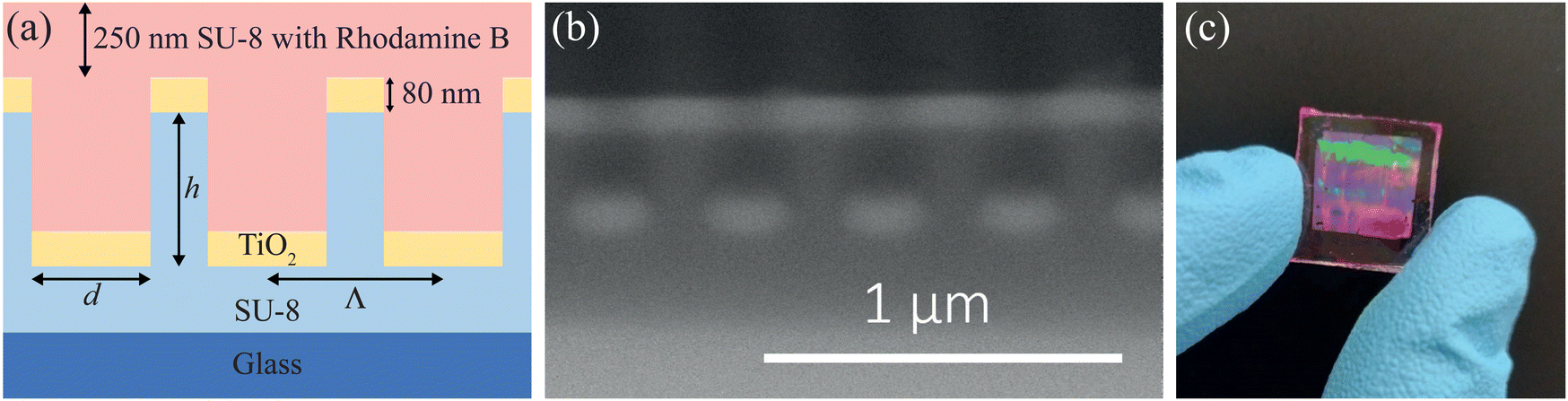 | ||
| Fig. 1 (a) Schematics of the system under study consisting of a SU-8 layer deposited on a microscope slide, which is patterned employing soft-lithography and covered by an evaporated TiO2 layer of 80 nm thickness. The lattice parameter of the system, Λ, ranges from 300 nm to 600 nm. The unit cell contains a hole of diameter d and height h. For the system with Λ = 300 nm, both d and h are 150 nm. For Λ = 400 and 500 nm, d = 300 nm and h = 350 nm, while for Λ = 600 nm, d = 330 nm and h remains at 350 nm. After its optical characterization, the system is coated with a rhodamine B-doped SU-8 layer, leaving a 250 nm thick superstrate. (b) Cross-sectional SEM micrograph of one sample before spin-coating the rhodamine B-doped SU-8 layer. (c) Photograph of one sample showing the typical iridescence. | ||
The different patterns used in this work were fabricated on SU-8 (SU-8 2000.5 Microchem) by means of soft nanoimprinting lithography at 95 °C using pre-patterned hybrid stamps. The elastomeric molds used herein consisted of a thin layer of rigid silicone and a polydimethylsiloxane (PDMS) back support, enabling a higher fidelity in the replication while maintaining flexibility.44 The patterned epoxy films were cured with UV light, hard baked, and subsequently covered with an 80 nm thick TiO2 layer by thermal evaporation (see Methods section). Examples of the resulting arrays, covering an area of 1 cm2, are shown in Fig. 1b and c. We chose TiO2 due to its HRI (∼2.2 to 2.4) and transparency in the visible range. The TiO2 coating contributes to enhancing the electromagnetic field within the nanostructures, enabling intense optical resonances that can be used for light emission enhancement.
For the realization of PL experiments, we covered all the samples with the gain medium (SU-8 2000.5 diluted in SU-8 thinner until 7 wt% mixed with rhodamine B). This dye can be efficiently excited with a 532 nm laser and has a high quantum yield. Solutions with concentrations ranging from 0.6 to 3 wt% were then spin-coated on top of the TiO2 layer in such a way that the solutions filled the holes and created a 250 nm-thick flat layer on top, as observed in AFM and SEM images (see Fig. S1 and S2, ESI†). In this case, the SU-8 was cured over time to avoid using UV light, which could deteriorate the rhodamine B.
Fig. 2 analyzes the optical response of samples with Λ = 300, 400, 500, and 600 nm. As a reference, we also analyze a disordered sample consisting of a random distribution of holes with d and h equal to 300 and 350 nm, respectively, and a minimal correlation distance of 500 nm. The black and blue curves in Fig. 2a show, respectively, the transmittance and reflectance spectra for the different periodicities under consideration before the addition of the dye-doped layer. These measurements were taken using an FTIR coupled to an optical microscope, under normal incidence from the top of the system (see Methods section). Examining the spectra of the ordered arrays, we observe that, in stark contrast to the disordered sample, these systems exhibit several prominent resonances, which have sharper and more pronounced lineshapes in transmittance than in reflectance. As Λ increases, these resonances redshift, suggesting their origin is linked to diffractive effects. Indeed, for the largest period under consideration, additional resonances, associated with higher diffraction orders, emerge in the spectrum around 500 nm. The optical response of these systems is more intricate than that of conventional arrays of discrete particles,10,27 since both the subarray of holes on the TiO2 top layer and the subarray of TiO2 disks deposited at the bottom of the holes can support optical resonances, whose characteristics are also largely influenced by interactions between them. This phenomenon likely accounts for the appearance and the characteristics of the different observed peaks.
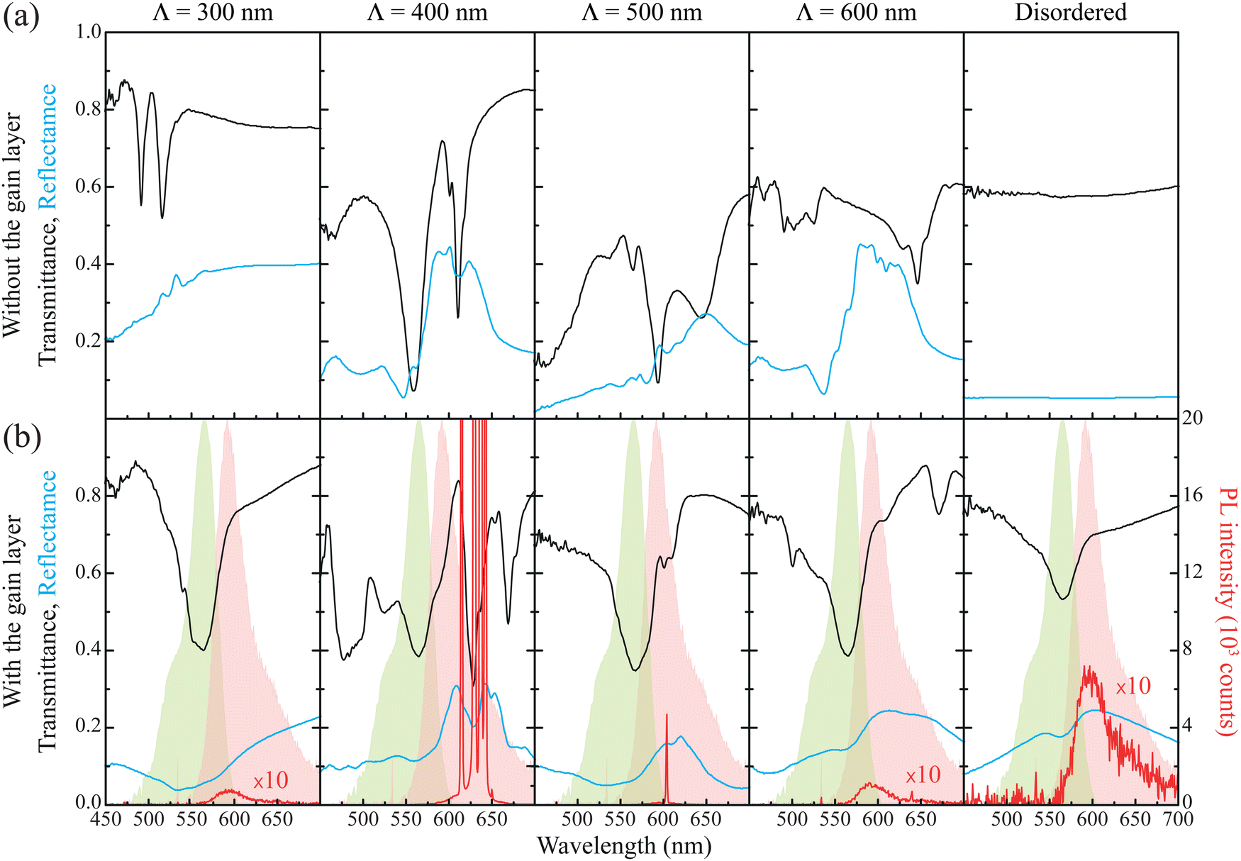 | ||
| Fig. 2 (a) and (b) Optical response of the 2D arrays without (a) and with (b) the rhodamine B-doped SU-8 layer. From left to right, the different panels correspond to Λ = 300, 400, 500, and 600 nm, and a disordered hole arrangement. The black and blue curves display, respectively, the transmittance and reflectance of the sample, while in (b), the red curve corresponds to its PL. The PL is measured using a single pulse of a 532 nm laser, with an energy density of 1.3 mJ cm−2. Importantly, the PL spectra of the arrays with Λ = 300 and 600 nm, and the disordered arrangement have been rescaled for better visibility. The green and red shaded areas indicate, respectively, the normalized absorption and emission spectra of a pristine layer of rhodamine B-doped SU-8. | ||
Fig. 2b shows the optical response of the same systems analyzed in Fig. 2a after coating them with the gain layer (3 wt% rhodamine B-doped SU-8). The addition of the gain layer has two main effects on the response of the arrays. First, it introduces a strong dip in the transmittance at 560 nm, which follows the profile of the absorption band of rhodamine B indicated by the green-shaded area. Second, the change in the refractive index of the medium above the array reshapes the transmittance and reflectance spectra, modifying both the spectral position and lineshape of the optical resonances. Fig. 2b also displays the PL spectra of the system, collected in the direction perpendicular to the array, for excitation at 532 nm with a single laser pulse of energy density of 1.3 mJ cm−2. Under these excitation conditions, the array with Λ = 400 nm shows the best lasing characteristics in terms of efficiency and threshold (0.1 mJ cm−2). This system sustains several diffractive modes arising from its periodic nature that overlap spectrally with the emission band of rhodamine B, marked by the red-shaded area. The system with Λ = 500 nm also achieves lasing, however, it sustains a single lasing mode with a higher threshold and lower efficiency (see Fig. S3, ESI†). The remaining arrays do not exhibit any relevant PL characteristics, regardless of the excitation energy density. We attribute this to the substantial detuning of their optical resonances relative to the emission band of rhodamine B. Similarly, the sample with the disordered arrangement of holes does not show any nonlinear PL characteristics for excitation energy densities ranging from 0.05 to 1.2 mJ cm−2.
Seeking more insight into the behaviour of the resonances sustained by the array, we performed an angular characterization of the transmittance and the PL spectra for the samples covered with the gain layer. To that end, we used a custom-made angular measurement setup comprising different light sources and a rotating stage (see Methods section). Fig. 3a–c shows the SEM images and the angle-resolved measurements of the best-performing array, Λ = 400 nm. As a reference, Fig. 3d–f displays the same information for the disordered sample. The SEM images shown in Fig. 3a and d correspond to the top surface of the original masters and illustrate the geometry of each sample. Examining the angle-resolved transmittance for the ordered array with Λ = 400 nm shown in Fig. 3b, we confirm the existence of several diffractive modes sustained by the structure. The wavelengths of these modes shift with increasing incidence angle, further confirming its diffractive nature. The rich optical response of this straightforwardly fabricated structure is directly tied to the complexity of its stratified geometry, consisting of three components layered on the corrugated surface (gain medium, TiO2, SU-8). In contrast, simpler geometries, such as disk arrays on a substrate or plates with holes, exhibit more limited optical responses, consistent with their two-dimensional confinement.10,27 For the disordered sample, as expected, the angle-resolved transmittance of Fig. 3e only shows the absorption band of rhodamine B.
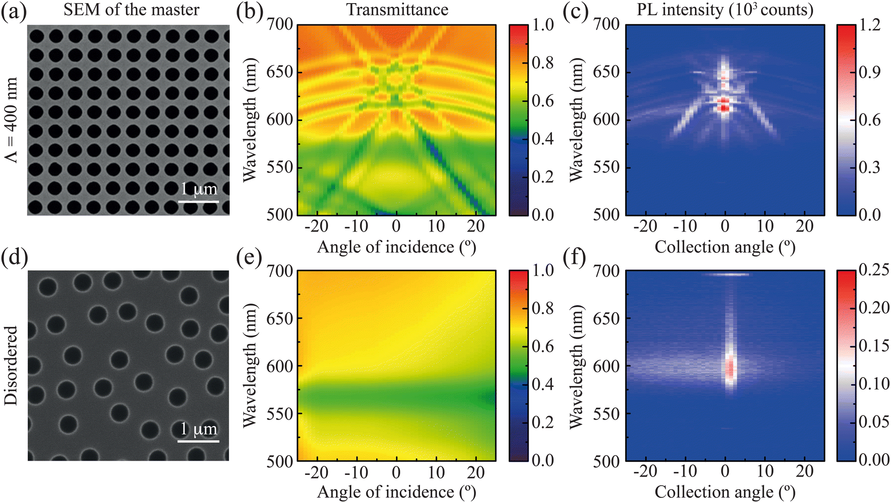 | ||
| Fig. 3 (a) SEM top-view of the master used to imprint the array with Λ = 400 nm. (b) and (c) Angle-resolved transmittance (b) and PL (c) for the array with Λ = 400 nm. (d)–(f) Same as (a)–(c) but for the disordered sample. | ||
The results for the angle-resolved PL shown in Fig. 3c and f, which were collected from the samples below the lasing threshold using 50 pulses of 0.05 mJ cm−2, follow the diffractive modes for the Λ = 400 nm array and exhibit no relevant features in the case of the disordered sample. The consistency between the angle-resolved transmittance and the PL for the ordered array highlights, once more, the important contribution of the diffractive modes sustained by the array. This observation supports the central role played by the periodic arrangement in achieving robust and controllable lasing, though the lattice parameter must be engineered so the modes of the array overlap with the emission range of the dye. Indeed, the smaller and larger values of Λ explored here do not offer a good matching with the emission band of rhodamine B, thus resulting in less efficient lasing characteristics. It is also worth noting that the disordered sample produced nearly three orders of magnitude fewer counts than the Λ = 400 nm array, indicating both weak amplification and inefficient outcoupling of the PL to the external medium.
To gain a deeper understanding of the arrays under study, we performed numerical simulations of their optical response using a finite element method (see Methods section). The solid green curve in Fig. 4a shows the transmittance of the Λ = 400 nm array calculated at normal incidence. We can distinguish four distinct dips centered at wavelengths 621, 628, 652, and 663 nm, which align well with the experimental spectrum indicated by the dashed black curve. However, the experimental results present two additional shoulders around 635 and 677 nm. We hypothesize that these resonances originate from inhomogeneities in the TiO2 coating arising, for instance, from a slight tilt during the physical deposition of the oxide, which break the C4 symmetry of the system and lift the polarization degeneracy expected for a square array.45 To verify this premise, we performed additional simulations of an array displaying an asymmetric deposition of TiO2 inside the hole, as depicted in the inset of Fig. 4a. This particular geometry is motivated by the top-view SEM image of the experimental system and the measurement of the polarization anisotropy of the array, which we show in Fig. S4a and b (ESI†). Analyzing the numerical results for the anisotropic system excited with y-polarized light (solid orange curve), we find the two additional modes that were absent in the spectrum of the isotropic system. This supports our hypothesis that the origin of these resonances is linked with the asymmetric deposition of TiO2 inside the hole. For excitation with x-polarized light (solid blue curve), we observe the emergence of an additional mode around 655 nm and the redshift of some of the resonances. This additional mode was also observed experimentally when the illumination spot was scanned across the sample, as shown in Fig. S4c (ESI†), while the redshift is an expected effect due to the presence of an additional volume of HRI dielectric inside the hole. For completeness, we calculated the angle-resolved transmittance for the isotropic system. The results, shown in Fig. 4b, are in good agreement with the measurements of Fig. 3b. They confirm the strength, the spectral position and the diffractive nature of the multiple modes supported by the system.
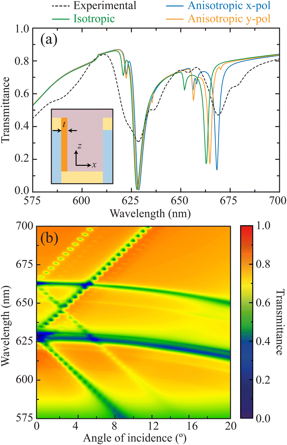 | ||
| Fig. 4 (a) Transmittance spectrum for the Λ = 400 nm array calculated with a finite element method. The green solid curve represents the results for the isotropic structure, while the solid blue and orange curves correspond to the anisotropic structure under excitation with x- and y-polarized light, respectively (see main text for details). The inset illustrates the geometry of the anisotropic structure used in the calculations. For reference, the dashed black curve indicates the experimental results. (b) Angle-resolved transmittance for the isotropic system calculated with a finite element method. | ||
To finalize the analysis of the arrays under study, we conducted a more in-depth characterization of the lasing performance of the Λ = 400 nm array. Specifically, we studied the evolution of the PL spectrum with increasing excitation energy density, as well as the directionality and the polarization of the emitted light. Fig. 5a shows the PL spectrum measured below the threshold with 50 pulses of 0.05 mJ cm−2, which displays relatively broad spectral features. However, as shown in Fig. 5b, when the energy density of the excitation is increased, the emission profile changes, revealing sharp peaks (FWHM < 1.5 nm) in the region between 610 and 650 nm and signaling the onset of lasing. This transition is clearly illustrated in Fig. 5c, which shows the characteristic non-linear behaviour of the PL intensity of each lasing mode as a function of the energy density of the excitation, indicating that each mode has a slightly different threshold. The difference in lasing thresholds and intensities of the lasing modes indicates that they compete for the energy present in the system.17 This is particularly relevant in our devices, where the large spatial and spectral overlap between the different modes explains the variation in the exact lasing wavelengths from sample to sample, although they consistently fall within the same wavelength range (see Fig. S5, ESI†). In any case, the HRI dielectric arrays studied in this work are able to sustain lasing across different optical modes with a low threshold, highlighting the robustness of this photonic structure against imperfections.
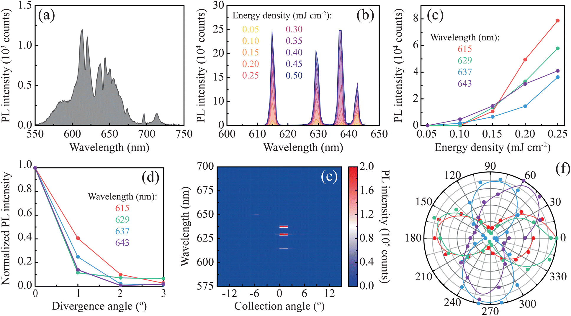 | ||
| Fig. 5 (a) PL spectrum of the Λ = 400 nm array below threshold, collected perpendicular to the system using 50 pulses with energy density 0.05 mJ cm−2. (b) PL spectra under lasing conditions for increasing excitation energy densities. (c) PL intensity at each mode peak wavelength as a function of the excitation energy density. (d) Divergence of the lasing modes of (b) when excited at 0.45 mJ cm−2. (e) Spectrally-resolved emission directionality of the PL above the lasing threshold. (f) Polarization analysis of the lasing modes of (b) when excited at 0.45 mJ cm−2. | ||
Fig. 5d and e analyze the characteristic high directionality (low divergence) of the laser emission, with the beam intensity rapidly dropping as the collection angle shifts away from the normal direction. Compared to the PL spectra below the threshold (Fig. 3c and 5a), the lasing regime exhibits an intense emission near 0°, while the dispersive behaviour of the modes remains hidden within the background (Fig. 5e). Besides, the emission is highly polarized, with different modes presenting distinct linear polarizations (see Fig. 5f). This result is consistent with the polarization anisotropy revealed in the measured (Fig. S4b, ESI†) and simulated (Fig. 4a) transmittance spectra. It is worth mentioning that pump polarization can influence the lasing properties of solid-state devices.46 However, in our system, as shown in Fig. 5f, both x- and y-polarized lasing modes are excited with similar efficiencies and thresholds, even for a linearly polarized excitation. This behaviour can be attributed to energy transfer between dye molecules occurring at sufficiently high concentrations,47 which homogenizes the orientation of their emission dipoles.
Many factors influence the threshold of a lasing system, one of which is the dye concentration in the gain layer. To account for this, we conducted a study, summarized in Fig. S6 (ESI†), in which the thickness of the gain layer was held constant while the concentration of rhodamine B was modified from 0.6 to 3 wt%. For 0.6 wt% concentration, a single sharp peak appears at 606 nm with a threshold of 1.2 mJ cm−2, while, for 1.5 wt%, three different modes are visible with thresholds around 0.4 mJ cm−2. This behaviour is typical for an organic multimode laser device. It is well-established that the laser threshold, particularly in 4-level laser systems, decreases with increasing concentration of gain material.48 Phenomenologically, higher concentrations enhance the absorption of pump photons, reducing the threshold. Interestingly, the threshold reduction applies to all photonic modes of the system. Therefore, at a given pump density, increasing the concentration can excite additional laser modes, provided they achieve population inversion. For a predominantly homogeneously broadened emitter like rhodamine B, this typically occurs when the lowest-threshold mode does not fully deplete the population inversion, leaving excess for other modes to utilize. However, excessively high concentrations can cause aggregation and intermolecular interactions that diminish the effective PL quantum yield and introduce optical inhomogeneities, which ultimately result in higher thresholds.48 It is worth noting that the HRI dielectric array studied in this work displays four lasing peaks with thresholds below 0.1 mJ cm−2. For comparison, a 2D array of metallic nanoparticles with the same gain medium (rhodamine B 3 wt% in 250 nm SU-8 matrix) displayed a lasing threshold of 30 mJ cm−2,11 which highlights the advantages that our system can provide for the development of lasing technologies.
2. Conclusions
We have designed a robust and easily produced photonic system that achieves multiband lasing with a low threshold. The structure, consisting of a square array of holes imprinted in an epoxy resin, coated with an HRI dielectric material and covered with gain media, was created using soft nanoimprinting lithography followed by the physical deposition of a TiO2 layer. By analyzing different 2D periodic arrays and a sample with a random distribution of holes, we demonstrated that the system whose modes aligned with the emission band of rhodamine B, supported multiband lasing, characterized by four bands in the range from 615 nm to 643 nm with thresholds as low as 0.1 mJ cm−2 for a 3 wt% rhodamine B concentration in a 250 nm film. Through angle- and polarization-resolved transmittance experiments and finite element method calculations, we showed that these diffractive modes originate from the periodic structure of the system and the asymmetries in the TiO2 coating, which break the polarization degeneracy of the square arrays. Our work demonstrates a method for creating lasing platforms based on HRI dielectrics with complex geometries using a simple and scalable fabrication approach. This approach yields robust optical responses suitable for multiband lasing, whose emission range is readily tunable through geometric adjustments. These advancements pave the way for cost-effective, scalable, and compact multimode lasing systems.3. Methods
3.1. Preparation of the PDMS stamps
The hard PDMS stamps were fabricated starting from original masters purchased from NAITEC (Λ = 300–600 nm) and CONSCIENCE AB (random). The masters were silanized using trichloro (1H,1H,2H,2H-perfluorooctyl) silane (97%, CAS: 78560-45-9) purchased from Sigma Aldrich. For the imprints, hybrid stamps combining a thin layer of hard polydimethylsiloxane (h-PDMS) and a flexible PDMS support were used. h-PDMS was prepared by components purchased from Gelest (CymitQuimica, Spain): 0.85 g of 7–8% vinylmethylsiloxane (CAS: 67762-94-1) were mixed with 25 μL of modulator (1,3,5,7-tetramethylcyclotetrasilane) (95%, CAS: 2370-88-9) and, while stirring the solution, 1.5 μL of catalyst (Platinum divinyltetramethyldisiloxane, CAS: 68478-92-2) were added, followed by 275 μL of hydroxyl siloxane (CAS: 68037-59-2) and 1 mL of toluene. The mixture was spread onto the masters with the aid of a compressed air gun, left at room temperature to homogenize the thickness of the layer, and later baked at 60 °C for 1 hour. Then, standard PDMS Sylgard 184 (Neyco) was added. Sylgard was prepared following the standard protocol of mixing 10 parts of Sylgard 184 pre-polymer to 1 part of curing agent and degassing the mixture for 1 hour. After adding it to the h-PDMS, the PDMS was cured at 100 °C. Once cooled down, the PDMS stamps were demolded.3.2. Preparation of the samples
Microscope glass slides (Labbox) were used as substrates and cleaned using ultrasonic baths of acetone (5 minutes), diluted Hellmanex III (3%) solution (5 minutes), isopropanol (5 minutes), and sodium hydroxide (10 minutes), and then rinsed with distilled water. The negative photoresist SU-8-2000.5 (14 wt% in thinner) from Microchem was spin-coated onto a glass slide at 2000 rpm for 30 s. The imprinting process was conducted on a hot-plate at 95 °C for a few seconds, during which the pre-patterned stamp was placed onto the resist. Upon heating beyond the glass transition temperature of the resist, the stamp sank into the film and the patterned PDMS filled with SU-8 became transparent. Next, the system was left to cool down and the PDMS was removed. The patterned SU-8 film was subsequently cured in UV light for 10 minutes and hard-baked at 120 °C for 2 hours, following the instructions to consolidate the structure provided by the manufacturer.The TiO2 films were prepared by evaporating TiO2 pellets (99.99% purity, purchased at Neyco.fr) from a graphite crucible with an electron beam evaporation system (Orion, from AJA international Inc.). During the evaporation of the film the pressure did not exceed 10−6 mbar and the base pressure was in the 10−8 mbar range. The deposition rate was monitored by a quartz crystal sensor and was kept in the order of 2 Å s−1. A Telemark ebeam source with a 10 KW power supply was used for this experiment.
To add the gain material, the samples were coated with a 250 nm-thick rhodamine B-doped film (SU-8 2000.5 diluted in SU-8 thinner until 7 wt%). The concentration of rhodamine B was calculated with respect to the solid content of SU-8 (i.e., assuming a complete evaporation of the solvent) and varied from 0.6 to 3 wt%, i.e., 15 to 75 mM.
3.3. Characterization of the transmittance and reflectance of the samples
Transmittance and reflectance measurements of the samples at normal incidence were conducted with an FTIR spectrophotometer (Vertex 70, Bruker) attached to an optical microscope (Hyperion) equipped with a 4X objective (0.1 NA) and unpolarized light. A silver mirror was used as a reference for reflectance measurements, while air was used as the reference for transmittance.Angle-resolved measurements were collected with the custom-made setup illustrated in Fig. S7 (ESI†). The sample was illuminated with a white light produced by a tungsten halogen lamp (Ocean Optics, HL-2000-HP, Florida, USA). Two filters (Edmund Optics, SCHOTT BG64, and Thorlabs, SRF11) were used to increase the signal in the UV and NIR region. The light was focused on the sample and collected using two achromatic doublet lenses (f = 100 mm and f = 50 mm). The detection system was mounted on a rotational optical breadboard (Thorlabs, RBB12A, New Jersey, USA), and the sample holder was positioned on a rotational stage (Ø = 50 mm) equipped with resonant piezoelectric motors (Thorlabs, ELL18/M), which were controlled via an interface board using LabVIEW. The sample was mounted vertically and oriented along the high symmetry direction of the arrays on a custom-made sample holder, allowing for precise control of the azimuthal angle φ (± 3°). The transmitted light was collected using a fiber-coupled spectrophotometer (Ocean Optics, QEPro-FL) with a range of detection 380–1200 nm.
3.4. Photoluminescence characterization of the samples
To measure PL, the samples were coated with a layer of 7 wt% SU-8 doped with rhodamine B (0.6–3.0 wt%). This layer was prepared using SU-8 2000.5 (Kayaku), diluted with SU-8-2000 thinner (MicroCHEM, Westborough, MA 01581), and rhodamine B dye powder purchased from Sigma Aldrich (RhB, CAS 81-89-9; MW 479.01 g mol−1). The same setup described above was used for the angle-resolved measurements, with the tungsten lamp replaced by a 1.5 ns pulsed 532 nm laser (CryLaS Gmb, Ostendstrasse 25, D-12459 Berlin, Germany) operating at a repetition rate of 100 Hz, with vertical polarization. To determine the lasing threshold, the excitation power was increased from 10 μW up to 240 μW, monitored using a power meter console (Thorlabs PM100D) coupled to a standard photodiode power sensor (Thorlabs S121C). Results were expressed in energy density, calculated as power divided by the repetition rate and the area of the laser spot. The diameter of the latter was measured to be around 500 μm using a beam profiler. The emitted PL was collected via a fiber coupled to a spectrophotometer (Ocean Optics, QEPro-FL), utilizing a reflective collimator (Thorlabs, RC08SMA-P01) and a long pass edge filter with high transmission (Semrock Edge basic BLP01-532R-25) to block the excitation laser-line. The entire setup was connected to a workstation, and a customized LabVIEW program was employed to manage the experiment.3.5. Numerical calculations
Maxwell's equations were rigorously solved using a finite element method implemented in the commercial software COMSOL Multiphysics. To model the periodic array, a domain corresponding to one unit cell was considered, and Floquet-periodic boundary conditions were employed. When possible, the symmetries of the system were exploited to further reduce the domain size by employing perfect electric and/or perfect magnetic conductor boundary conditions. The simulation domain was truncated in the direction perpendicular to the array using perfectly matching layers. The refractive index of SU-8 and glass were taken as 1.59 and 1.52, respectively; the value for TiO2 was obtained from literature,49 while the refractive index of the SU-8 layer doped with rhodamine B was measured in the laboratory. The values of all geometrical parameters were kept consistent with those indicated in the caption of Fig. 1, unless otherwise stated. The diameter was reduced from the initially assumed value of 300 nm to 270 nm to optimize the agreement between simulations and experiments. This variation corresponds to 10% of the initial value, which falls within the experimental uncertainty of fabrication. For the simulation of the anisotropic system, we introduce an additional layer of TiO2 with the shape of a semicylindrical shell and a thickness t = 9.45 nm (see inset in Fig. 4).Data availability
The data supporting this article have been included as part of the ESI.†Conflicts of interest
There are no conflicts to declare.Acknowledgements
This project has received funding from the EIC PATHFINDER OPEN project 101046489 (DYNAMO), funded by the European Union. This research was also supported by the Spanish Agencia Estatal de Investigación (MICIU/AEI/10.13039/501100011033) through the I + D + I project CEX2023-001263-S (Spanish Severo Ochoa Centre of Excellence program), PID2022-141956NB-I00, and PID2022-137569NB-C42, as well as the Generalitat de Catalunya (2021-SGR-00444). A. C.-R. acknowledges support from the postdoctoral fellowship program Beatriu de Pinós 2022 BP 00083, funded by the Secretary of Universities and Research (Government of Catalonia), partially funded by H2020-MSCA-COFUND-2022 through grant agreement 801370. J.R.D-R. acknowledges support from a predoctoral fellowship from the MCIN/AEI assigned to PID2019-109502GA-I00. L.C. acknowledges support from a Ramón y Cajal Research Fellowship, Grant RYC2022-038362-I, funded by MCIN/AEI/10.13039/501100011033 and by the European Social Fund Plus (ESF+).References
- C.-Z. Ning, Adv. Photonics, 2019, 1, 014002 Search PubMed.
- A. S. Sarkar, I. Konidakis, I. Demeridou, E. Serpetzoglou, G. Kioseoglou and E. Stratakis, Sci. Rep., 2020, 10, 1 CrossRef.
- R.-M. Ma and R. F. Oulton, Nat. Nanotech, 2019, 14, 12 CrossRef CAS PubMed.
- Y. Liang, C. Li, Y.-Z. Huang and Q. Zhang, ACS Nano, 2020, 14, 14375 CrossRef CAS PubMed.
- S. I. Azzam, A. V. Kildishev, R.-M. Ma, C.-Z. Ning, R. Oulton, V. M. Shalaev, M. I. Stockman, J.-L. Xu and X. Zhang, Light: Sci. Appl., 2020, 9, 90 CrossRef CAS.
- V. G. Kravets, A. V. Kabashin, W. L. Barnes and A. N. Grigorenko, Chem. Rev., 2018, 118(12), 5912–5951 CrossRef CAS.
- W. Wang, M. Ramezani, A. I. Väkeväinen, P. Törmä, J. G. Rivas and T. W. Odom, Mater. Today, 2018, 21, 303 CrossRef.
- A. D. Utyushev, V. I. Zakomirnyi and I. L. Rasskazov, Rev. Phys., 2021, 6, 100051 CrossRef.
- L. Zundel, J. R. Deop-Ruano, R. Martinez-Herrero and A. Manjavacas, ACS Omega, 2022, 7, 31431 CrossRef.
- A. Yang, T. B. Hoang, M. Dridi, C. Deeb, M. H. Mikkelsen, G. C. Schatz and T. W. Odom, Nat. Commun., 2015, 6, 6939 CrossRef PubMed.
- Y. Conti, N. Passarelli, J. Mendoza-Carreño, L. Scarabelli and A. Mihi, Adv. Opt. Mater., 2023, 11, 2300983 CrossRef.
- A. Manjavacas, L. Zundel and S. Sanders, ACS Nano, 2019, 13, 10682 CrossRef.
- D. Wang, A. Yang, W. Wang, Y. Hua, R. D. Schaller, G. C. Schatz and T. W. Odom, Nat. Nanotechnol., 2017, 12, 889 CrossRef.
- F. Freire-Fernández, T. Reese, D. Rhee, J. Guan, R. Li, R. D. Schaller, G. C. Schatz and T. W. Odom, ACS Nano, 2023, 17, 21905 CrossRef PubMed.
- A. Cuartero-González, S. Sanders, L. Zundel, A. I. Fernández-Domínguez and A. Manjavacas, ACS Nano, 2020, 14, 11876 CrossRef PubMed.
- M. P. Knudson, R. Li, D. Wang, W. Wang, R. D. Schaller and T. W. Odom, ACS Nano, 2019, 13, 7435 CrossRef PubMed.
- R. Heilmann, K. Arjas, T. K. Hakala and P. Törmä, ACS Photonics, 2023, 10, 3955 CrossRef.
- I. Staude, T. Pertsch and Y. S. Kivshar, ACS Photonics, 2019, 6, 802 CrossRef.
- Z. Zhai, Z. Li, Y. Du, X. Gan, L. He, X. Zhang, Y. Zhou, J. Guan, Y. Cai and X. Ao, ACS Photonics, 2023, 10, 437 CrossRef.
- J.-H. Yang, Z.-T. Huang, D. N. Maksimov, P. S. Pankin, I. V. Timofeev, K.-B. Hong, H. Li, J.-W. Chen, C.-Y. Hsu, Y.-Y. Liu, T.-C. Lu, T.-R. Lin, C.-S. Yang and K.-P. Chen, Laser Photonics Rev., 2021, 15, 2100118 CrossRef CAS.
- M. Wu, S. T. Ha, S. Shendre, E. G. Durmusoglu, W.-K. Koh, D. R. Abujetas, J. A. Sánchez-Gil, R. Paniagua-Domínguez, H. V. Demir and A. I. Kuznetsov, Nano Lett., 2020, 20, 6005 CrossRef CAS PubMed.
- M. Decker and I. Staude, J. Opt., 2016, 18, 103001 CrossRef.
- G. W. Castellanos, P. Bai and J. Gómez Rivas, J. Appl. Phys., 2019, 125, 213105 CrossRef.
- S. Murai, G. W. Castellanos, T. V. Raziman, A. G. Curto and J. G. Rivas, Adv. Opt. Mater., 2020, 8, 1902024 CrossRef CAS.
- H. Alhalaby, H. Zaraket and M. Principe, Results Opt., 2021, 3, 100073 CrossRef.
- S. I. Azzam, K. Chaudhuri, A. Lagutchev, Z. Jacob, Y. L. Kim, V. M. Shalaev, A. Boltasseva and A. V. Kildishev, Laser Photonics Rev., 2021, 15, 2000411 CrossRef CAS.
- M. Higashino, S. Murai, T.-Y. Lo, S. Tomita and K. Tanaka, J. Mater. Chem. C, 2022, 10, 9730 RSC.
- M. Wu, L. Ding, R. P. Sabatini, L. K. Sagar, G. Bappi, R. Paniagua-Domínguez, E. H. Sargent and A. I. Kuznetsov, Nano Lett., 2021, 21, 9754 CrossRef CAS PubMed.
- O. Aftenieva, M. Sudzius, A. Prudnikau, M. Adnan, S. Sarkar, V. Lesnyak, K. Leo, A. Fery and T. A. F. König, Adv. Opt. Mater., 2023, 11, 2202226 CrossRef CAS.
- J. Guan, L. K. Sagar, R. Li, D. Wang, G. Bappi, W. Wang, N. Watkins, M. R. Bourgeois, L. Levina, F. Fan, S. Hoogland, O. Voznyy, J. M. de Pina, R. D. Schaller, G. C. Schatz, E. H. Sargent and T. W. Odom, ACS Nano, 2020, 14, 3426 CrossRef CAS.
- C. Fruhling, K. Wang, S. Chowdhury, X. Xu, J. Simon, A. Kildishev, L. Dou, X. Meng, A. Boltasseva and V. M. Shalaev, Laser Photonics Rev., 2023, 17, 2200314 CrossRef CAS.
- A. L. Alvarado-Leaños, D. Cortecchia, C. N. Saggau, S. Martani, G. Folpini, E. Feltri, M. D. Albaqami, L. Ma and A. Petrozza, ACS Nano, 2022, 16, 20671 CrossRef PubMed.
- Y. Li, H. Zhou, M. Xia, H. Shen, T. Wang, H. Gao, X. Sheng, Y. Han, Z. Chen, L. Dou, H. Zhu and E. Shi, Sci. Adv., 2023, 9, eadh0517 CrossRef CAS.
- Y.-H. Hsieh, B.-W. Hsu, K.-N. Peng, K.-W. Lee, C. W. Chu, S.-W. Chang, H.-W. Lin, T.-J. Yen and Y.-J. Lu, ACS Nano, 2020, 14, 11670 CrossRef PubMed.
- Y. Shang, J. Zhou, Y. Cai, F. Wang, A. Fernandez-Bravo, C. Yang, L. Jiang and D. Jin, Nat. Commun., 2020, 11, 6156 CrossRef.
- Y. Shang, T. Chen, T. Ma, S. Hao, W. Lv, D. Jia and C. Yang, J. Rare Earths, 2022, 40, 687 CrossRef.
- N. B. Tomazio, L. D. Boni and C. R. Mendonca, Sci. Rep., 2017, 7, 8559 Search PubMed.
- L. Cerdán, J. R. Deop-Ruano, J. J. Alvarez-Serrano and A. Manjavacas, Adv. Opt. Mater., 2024, 12, 2302737 CrossRef.
- V. E. Babicheva and A. B. Evlyukhin, Laser Photonics Rev., 2017, 11, 1700132 CrossRef.
- M.-S. Hwang, H.-C. Lee, K.-H. Kim, K.-Y. Jeong, S.-H. Kwon, K. Koshelev, Y. Kivshar and H.-G. Park, Nat. Commun., 2021, 12, 4135 CrossRef.
- Y. Gong, S. Wong, A. J. Bennett, D. L. Huffaker and S. S. Oh, ACS Photonics, 2020, 7, 2089 CrossRef.
- Z. Feng, T. Shi, G. Geng, J. Li, Z.-L. Deng, Y. Kivshar and X. Li, eLight, 2023, 3, 21 CrossRef.
- S. Balslev, T. Rasmussen, P. Shi and A. Kristensen, J. Micromech. Microeng., 2005, 15, 2456 CrossRef.
- J. A. Rogers and H. H. Lee, Unconventional Nanopatterning Techniques and Applications, John Wiley & Sons, Ltd, 2008 Search PubMed.
- C. Matricardi, J. L. Garcia-Pomar, P. Molet, L. A. Pérez, M. I. Alonso, M. Campoy-Quiles and A. Mihi, Adv. Opt. Mater., 2020, 8, 2000786 CrossRef.
- I. Gozhyk, M. Boudreau, H. R. Haghighi, N. Djellali, S. Forget, S. Chénais, C. Ulysse, A. Brosseau, R. Pansu, J.-F. Audibert, S. Gauvin, J. Zyss and M. Lebental, Phys. Rev. B: Condens. Matter Mater. Phys., 2015, 92, 214202 CrossRef.
- M. N. Berberan-Santos, E. J. Nunes Pereira and J. M. G. Martinho, J. Chem. Phys., 1997, 107, 10480 CrossRef.
- A. Palatnik, O. Bitton, H. Aviv and Y. R. Tischler, Opt. Mater. Express, 2016, 6, 2715 CrossRef CAS.
- S. Sarkar, V. Gupta, M. Kumar, J. Schubert, P. T. Probst, J. Joseph and T. A. F. König, ACS Appl. Mater. Interfaces, 2019, 11, 13752 CrossRef CAS PubMed.
Footnote |
| † Electronic supplementary information (ESI) available. See DOI: https://doi.org/10.1039/d4nh00574k |
| This journal is © The Royal Society of Chemistry 2025 |