
 Open Access Article
 This Open Access Article is licensed under a
 Creative Commons Attribution 3.0 Unported Licence
One-dimensional molecular nanostructures interacting with two-dimensional metals†
Pavel
Kocán
 *a,
Barbara
Pieczyrak
b,
Soshiro
Umachi
c,
Martin
Cigánek
d,
Pavel
Sobotík
a,
Ivan
Ošťádal
a,
Leszek
Jurczyszyn
b,
Jozef
Krajčovič
d and
Kazuyuki
Sakamoto
c
*a,
Barbara
Pieczyrak
b,
Soshiro
Umachi
c,
Martin
Cigánek
d,
Pavel
Sobotík
a,
Ivan
Ošťádal
a,
Leszek
Jurczyszyn
b,
Jozef
Krajčovič
d and
Kazuyuki
Sakamoto
c
aFaculty of Mathematics and Physics, Charles University, Prague, Czech Republic. E-mail: pavel.kocan@mff.cuni.cz
bInstitute of Experimental Physics, University of Wroclaw, Wroclaw, Poland
cDepartment of Applied Physics, Osaka University, Osaka, 565-0871, Japan
dBrno University of Technology, Faculty of Chemistry, Materials Research Centre, Purkyňova 118, 612 00, Brno, Czech Republic
First published on 12th February 2025
Abstract
Electrons confined within the 2D layer of metals grown on silicon substrates exhibit exotic properties due to strong correlation effects. Their properties, such as their 2D superconductivity, have been frequently subjected to possible tuning by doping using charge transfer from adsorbed layers. Doping relies on adding electrons or holes to the system and the resulting shift of the Fermi level EF in the otherwise robust surface electronic structure. This strategy has not been sufficiently controlled in the case of an indium double layer grown on the Si(111) surface. This study provides an alternative approach relying on spatially periodic modification of the surface electronic structure of the 2D metal. Derivatives of diketopyrrolopyrroles (DPP) are used for the growth of perfectly ordered 1D-like molecular superstructures on top of the In double layer, imaged by scanning tunneling microscopy. The integral changes of electronic structure are measured by angle-resolved photoelectron spectroscopy and density functional theory calculations show local modification of the surface states near EF by the adsorbed molecules. This study demonstrates that the surface electronic states can be controllably patterned, using a proper bonding scheme. It is anticipated that the combination of the original 2D superconductor and the 1D-like patterning will motivate further research.
New conceptsWe provide a strategy to confine the electronic states of a 2D metal layer by interaction with self-ordered 1D molecular nanostructures. The molecules create on the surface well ordered molecular wires with a length-to-width ratio of ∼103 driven by interaction via pairs of hydrogen bonds, as observed by scanning tunneling microscopy. Growing structures with desirable effects can be controlled by a choice of organic molecules and deposition conditions. Angle-resolved photoelectron spectroscopy shows that the electronic interaction of the surface with the molecules is gentle-enough to preserve the overall electronic structure. Simultaneously, the density of states of the metal layer at positions of the adsorbed molecules is modified according to density functional theory calculations. So far, the modification of the electronic states of the 2D metals was considered only by net doping – by a charge transfer from the adsorbed layer of the molecules. Here, we show that long-range ordered 1D molecular structures affect the density of 2D metallic states locally. This likely brings new functionalities, as is usual when decreasing the dimensionality of the system. The anisotropic patterning of the 2D electronic states creates a new class of materials, in which a 2D electron gas is interacting with the 1D modulation of the molecular adsorbate. |
Introduction
Termination of a semiconductor crystal by a 2D atomic layer breaks the spatial inversion symmetry along the surface normal direction. Together with spin–orbit coupling (SOC), the broken symmetry results in nontrivial phenomena. Complex electronic and spin structures have been reported in the last decade, with promising applications in future electronics, spintronics1 or valleytronics.2Layers of 5p or 6p metals (In, Bi, Tl or Pb) grown under ultra-high vacuum (UHV) conditions on silicon substrates show physical properties of 2D metals. These multivalent elements can both saturate surface dangling bonds with pz orbitals and create 2D metallic states via px and py orbitals. Their rich electronic properties arise from a complex SOC. A 2D electron gas often forms in these materials ( ,3
,3 ,4
,4 5) providing highly mobile electrons with a parabolic dispersion relation in the k-space.
In addition, Rashba-type spin splitting appears in these 2D metals due to the high electric fields present in the near-surface region. This effect was observed by angle-resolved photoemission spectroscopy (ARPES) and explained by density functional theory (DFT) for  ,6 Si(111)–Tl(1 × 1)2,7 or Si(110)–Tl(1 × 1).8
For the  surface used in this study,9,10 2D superconductivity has been reported11,12 and later explained by dynamic spin-momentum locking, which protects breaking of the Cooper pairs.13 There were attempts to increase the superconducting transition temperature TC ∼ 3 K by hole doping from an extra layer of organic molecules on top of the atomic layer. A nontrivial behavior was observed for phthalocyanine layers on top of the
  surface.6,14,15 Depending on the coordinated metal atom of the phthalocyanine, TC can be modified to lower or higher temperatures.6,14 With increasing amount of copper phthalocyanines on the surface, the TC at first increased to decrease again above the full layer,6 accompanied by increasing and decreasing hole doping as observed by ARPES.14 Deposition of the 3,4,9,10-perylenetetracarboxylic dianhydride (PTCDA) molecules with even higher electron affinity surprisingly led to lower TC, which was explained by insufficient ordering of the molecular layer.16
The possibilities of inter-molecular bonding are rather limited on 2D metal layers. Covalent bonding17via Ullmann coupling or metal coordinated bonding18 typically used on coin-age metals are complicated to realize on 5p or 6p 2D metals, because of the lack of catalytic properties of these metals. The temperature stability of 2D metals may limit thermal activation of the molecular precursors. For example, indium begins to desorb at ∼400 °C from the Si(111) surface, forming different non-2DEG structures. Therefore, we have chosen the stabilization of superstructures by intermolecular hydrogen bonds without the need for thermal activation.19
In this paper, we focus on interaction of the  surface with strongly one-dimensional molecular superstructures formed by functionalized diketopyrrolopyrrole (DPP) molecules. We go behind the simplification of the band doping and study the influence of the molecular superstructures on a local level.20–22 We demonstrate that by the local interactions, the pattern of molecular assemblies23 can be inprinted to the 2D metal layer.
DPP-based derivatives are pigments used as organic semiconductors24 in many fields of organic electronics, such as organic field-effect transistors or organic photo-voltaic devices.25 The DPP derivatives are highly versatile due to a wide range of their possible functionalization influencing its opto-electronic properties. The derivatives used here (Fig. 1, full chemical structures are in ESI†) can form 1D chains connected by pairs of hydrogen bonds, as demonstrated at the liquid–solid interface with the molecules in a solution.26 We use scanning tunneling microscopy (STM) to investigate the influence of molecular side groups on their self-ordering and ARPES to quantify changes in the electronic structure of the atomic layer. Details of the interaction are further analyzed by DFT calculations.
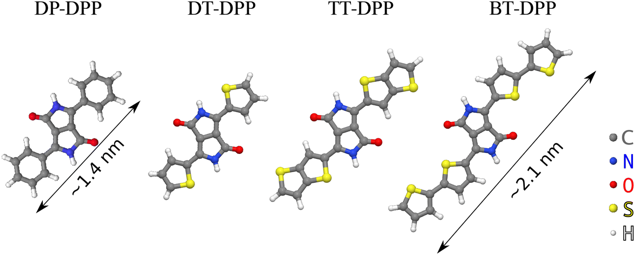 | ||
| Fig. 1 Derivatives used in the study. Diphenyl- (DP-), dithienyl- (DT-), dithieno[3,2-b] thienyl- (TT-) and dibithienyl- (BT-) diketopyrrolopyrrole (DPP). | ||
Results and discussion
Fig. 2 summarizes the STM results obtained upon UHV deposition of the DPP derivatives shown in Fig. 1 on the surface at room temperature. Fig. 2a–c shows the evolution of the morphology with increasing amount of deposited DP–DPP molecules. Even at low coverages (Fig. 2a), elongated molecular islands are observed, with length limited by the size of atomic terraces (∼500 nm). The width of the islands increases with coverage (Fig. 2b and c). Fig. 2d shows details of the molecular structure of a selected island. Each molecule can be easily distinguished and a model of the structure can be constructed, confirming double hydrogen bonds between adjacent molecules. Note that the DPP molecules become chiral when adsorbed on the surface, but all molecules in one chain are the same enantiomers (see Fig. 2d where ‘L’ and ‘R’ denote left- and right-enantiomers).
 | ||
| Fig. 2 STM images of DPP structures. (a)–(d) DP–DPP molecules forming elongated islands, (d) details of molecular alignment with denoted ‘L’ and ‘R’ enantiomers. (e)–(h) DT–DPP molecules forming single-molecule wide chains, (h) details of molecular alignment, (i) TT–DPP and (j) BT–DPP. Applied sample voltages: (a) +1 V, (b), (d) and (i) −1 V, (c), (f)–(h) −2 V, (e) and (j) −2.5 V. | ||
The morphologies of the structures prepared by deposition of DT–DPP molecules are shown in Fig. 2e–h. Even at very low coverage (Fig. 2e), long single-molecule wide chains are observed. The inset in Fig. 2e shows the details of one chain, revealing the corrugation corresponding to single molecules. With increasing coverage, the structure of the chains remain the same, but their density increases. On each atomic terrace, the wires order in parallel to allow the longest possible chains. Fig. 2h shows details of the surface almost fully covered by DT–DPP molecules.
Fig. 2i and j show the ordered molecular structures prepared by deposition of TT– and BT–DPP, respectively. In both cases, the scheme remains the same as in the case of DP–DPP molecules, and only the periodicity reflects the different size of the molecules.
Changes of electronic structure of the  layer caused by molecular adsorption were detected by ARPES in the case of representative DP- and DT–DPP molecules. The results are summarized in Fig. 3. Schematic representation of the Brillouin zones (BZs) is depicted in Fig. 3a. The
  BZ is marked in green and the 1 × 1 BZ of the idealized In top layer, which is responsible for the superconductivity, is marked by red rectangles. The radius of the circular feature of the Fermi surface (FS) originating from nearly free electrons in the top In layer (marked by violet circles in Fig. 3a) can be used as a measure of hole doping of the layer: with more holes provided to the system, the parabolic band of 2D free electrons shifts up, resulting in a decrease of radius of the circular feature at FS. Fig. 3b–d show the FS measured in the area marked by a blue rectangle in Fig. 3a, for the pristine
  surface (b) and for a full adsorbed ML of DP–DPP (c) and DT–DPP (d). The change of the radius upon adsorption ΔkFS can be obtained from fitting momentum distribution curves (MDC) calculated by summation of the photoelectron intensity within the window 0 ± 0.025 Å−1 displayed in Fig. 3e. The colors of MDC in Fig. 3e correspond to the colors of the open circles in Fig. 3b–d indicating the positions of the circular features at FS. By fitting the MDCs using Lorentzian curves, shifts of 0.0022 ± 0.0004 Å−1 and 0.010 ± 0.002 Å−1 were obtained for DP–DPP and DT–DPP molecules, respectively. Fitting the 4d core-level spectra (Fig. 3f) provides another way to obtain the level of doping. In the case of DP– and DT–DPP full monolayers, the energy shifts compared to the pristine surface were −15 ± 7 meV and 23 ± 7 meV, respectively. Compared to the shift of 40 meV in the case of copper phthalocyanine,6 this again shows that the hole doping is insignificant in the case of DP–DPP, but becomes reasonable in the case of adsorption of DT–DPP. The number of transferred carriers can be obtained from the change of radius of the Fermi surface by comparing the size of the Brillouin zone and the change of wave number. The resultant transferred holes per In atom are 0.005 ± 0.001 for DP–DPP and 0.024 ± 0.005 for DT–DPP molecules, respectively.
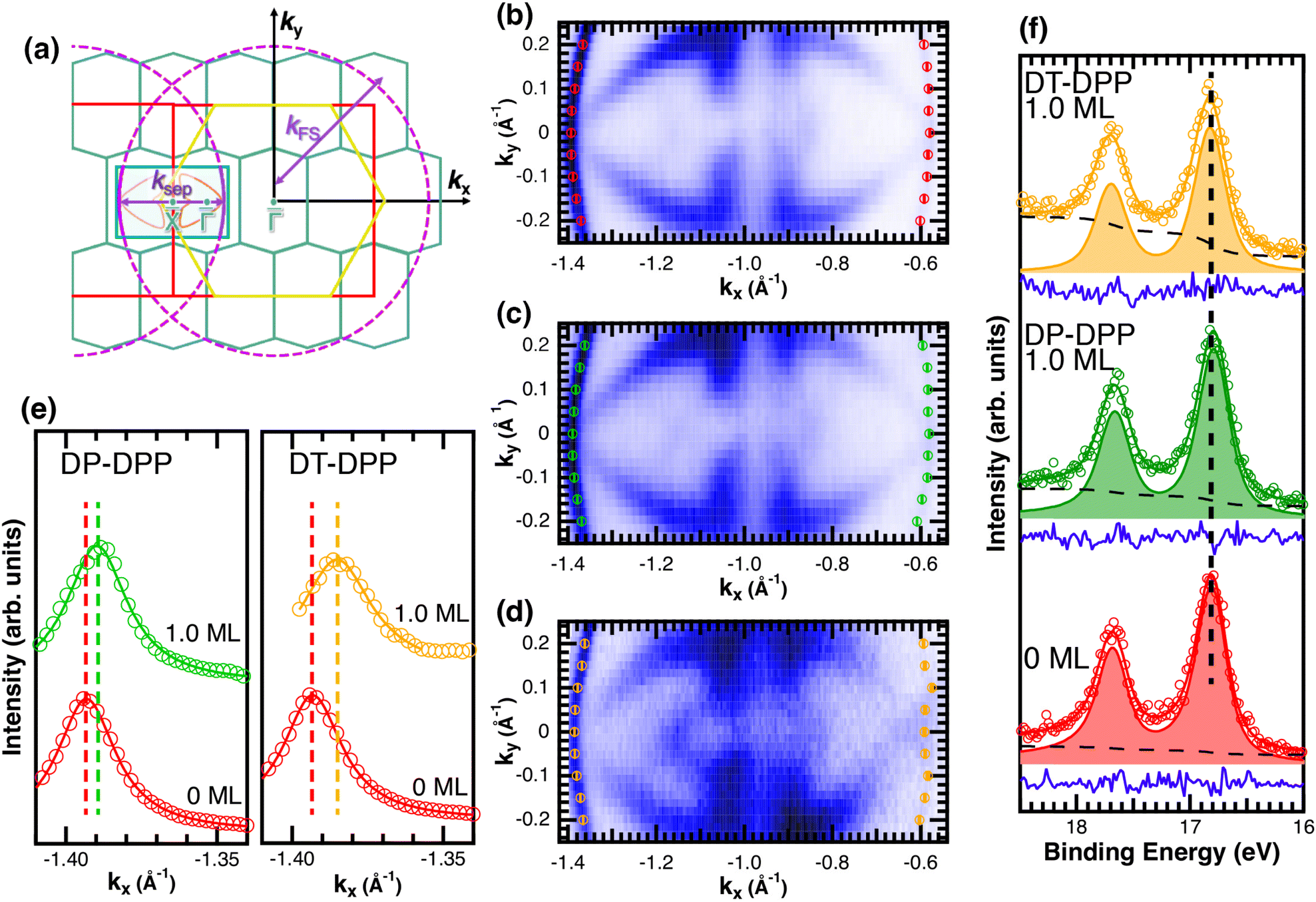 | ||
Fig. 3 ARPES results. The Brillouin zones (BZs) and schematic FSs are shown in (a). The  BZ, the Si(111)–(1 × 1) BZ, and the idealized (1 × 1) BZ of the In layer are indicated by green lines, yellow lines, and red lines, respectively. The violet dashed lines and the orange lines are the circular-shaped FSs and butterfly-shaped FSs of BZ, the Si(111)–(1 × 1) BZ, and the idealized (1 × 1) BZ of the In layer are indicated by green lines, yellow lines, and red lines, respectively. The violet dashed lines and the orange lines are the circular-shaped FSs and butterfly-shaped FSs of  . The blue rectangle indicates the area of the FSs measured using ARPES. KFS is the radius of the circular-shaped FS, and Ksep is the distance between two circular-shaped FSs that we measured to discuss the amount of charge doping. (b) shows the FS of a pristine . The blue rectangle indicates the area of the FSs measured using ARPES. KFS is the radius of the circular-shaped FS, and Ksep is the distance between two circular-shaped FSs that we measured to discuss the amount of charge doping. (b) shows the FS of a pristine  surface, and (c) and (d) are the FSs of surface, and (c) and (d) are the FSs of  fully covered by DP–DPP and DT–DPP, respectively. The open circles in (b)–(d) mark positions of the circular-shaped FSs obtained by MDCs measured at different ky. (e) shows the MDCs of the circular-shaped FSs of a pristine and DP–DPP and DT–DPP covered fully covered by DP–DPP and DT–DPP, respectively. The open circles in (b)–(d) mark positions of the circular-shaped FSs obtained by MDCs measured at different ky. (e) shows the MDCs of the circular-shaped FSs of a pristine and DP–DPP and DT–DPP covered  . The MDCs were obtained by the summation of the photoelectron intensity within a ky range of 0 ± 0.025 Å−1. The open circles are the experimental data, and the solid lines overlapping them show the Lorentzian fittings. (f) In 4d core-level spectra of pristine (bottom), DP–DPP (middle) and DT–DPP (top) covered surfaces. . The MDCs were obtained by the summation of the photoelectron intensity within a ky range of 0 ± 0.025 Å−1. The open circles are the experimental data, and the solid lines overlapping them show the Lorentzian fittings. (f) In 4d core-level spectra of pristine (bottom), DP–DPP (middle) and DT–DPP (top) covered surfaces. | ||
Structural properties of the molecules adsorbed on the  surface and their effect on the local electronic properties of the layer have been investigated using DFT. A relaxed structure of the surface fully covered by DT–DPP molecules is shown as top- and side-views in Fig. 4a and b. The structure is stabilized by a pair of O⋯HN hydrogen bonds. To evaluate this interaction, we have calculated several models with varying number of molecules in the case of DP– and DT–DPP molecules. The resultant hydrogen-bonding energies are −0.70 and −0.71 eV per pair of hydrogen bonds and the bonding energies to the substrate in the case of isolated molecules are −1.81 and −1.56 eV, respectively (for detailed analysis see the ESI†). The interaction energy between DPP molecules, crucial for formation of the linear chains, has been previously calculated using graphite as the substrate. Fu et al.26 obtained a somewhat higher value of ∼ −0.9 eV, probably due to a different competition between an ideal hydrogen bonding configuration and the optimal interaction with the surface.
 | ||
Fig. 4 DFT results. (a) and (b) Top and side view of a full monolayer of DT–DPP molecules on the  surface, as optimized by DFT. The side view shows only the two topmost silicon atomic layers. Electron density depletion and accumulation are shown by cyan and yellow, respectively. (c) The plane-integrated charge transfer. (d) LDOS projected to the top-most In atoms, as affected by adsorbed molecules compared to the pristine layer. (e) and (f) LDOS projected to single atoms below the molecule (e) and far from the molecule (f); the In atoms are indicated by blue and green arrows in (g). surface, as optimized by DFT. The side view shows only the two topmost silicon atomic layers. Electron density depletion and accumulation are shown by cyan and yellow, respectively. (c) The plane-integrated charge transfer. (d) LDOS projected to the top-most In atoms, as affected by adsorbed molecules compared to the pristine layer. (e) and (f) LDOS projected to single atoms below the molecule (e) and far from the molecule (f); the In atoms are indicated by blue and green arrows in (g). | ||
Cyan and yellow colors in Fig. 4a and b represent electron density depletion and accumulation, respectively, caused by adsorption of the molecules. The charge reorganization is strongly localized to the molecules, with charge depletion (light-blue color) near the topmost In layer and complex reorganization within the molecule. The plane-integrated charge transfer is shown in Fig. 4c. Similar to other systems,14,27 there is a net charge transfer from the area near the metal layer partially towards the molecules and partially towards the metal layer.
As the changes of electronic structure shown in Fig. 4a and b are rather complex, we proceed by plotting the local density of states (LDOS) projected to the top-most In atoms, as affected by adsorbed molecules compared to the pristine  layer, see Fig. 4d. To make the projections as comparable as possible, we used large slabs with a single adsorbed molecule of DPP derivatives shown in Fig. 1 per slab. The plotted LDOS are averaged over all In atoms in the topmost In layer. The electronic structure is indeed modified, with all DPP molecules showing a similar effect, somewhat more pronounced in the case of DT–DPP. For additional projections to atoms of molecules, see Fig. S4 in the ESI.†Fig. 4e and f show a comparison of LDOS projected to selected atoms affected and non-affected by the adsorbed DT–DPP molecule. In Fig. 4e and f the selected atom is directly under the central part of the DT–DPP molecule and in the area far from the molecule, respectively. The corresponding In atoms are marked in Fig. 4g by blue and green arrows. In each case, the LDOS is compared to that of the same In atom in the slab without adsorbed molecules (note that the LDOS of In atoms in the clean
  shows some variations due to its different positions with respect to the unit cell). Evidently, while the LDOS is preserved on the unoccupied area, it changes significantly under the molecule. The dominant occupied state at ∼ −0.8 eV and the state at the Fermi level shift by ∼0.2 eV towards empty states. The empty state at ∼1.5 eV is significantly reduced. The changes correspond to the complex charge redistribution presented in Fig. 4a and b. Projection of the LDOS in Fig. 4e and f to s- and p-orbitals (Fig. S5 of ESI†) shows that most changes due to adsorption of DPP molecules are related to s- and pz-orbitals. Additional LDOS curves for other studied DPP derivatives are shown in the ESI.†
Next, we discuss how the 1D chains of ordered molecules influence the surface electronic structure. Using DFT calculations, we have demonstrated that quasi-isolated molecules influence the electronic states locally. We propose that this effect would be similar in the case of the 1D chains, such as those in Fig. 2e. DFT calculations of slabs containing rows of molecules together with a bare surface would require extremely large supercells (∼2 × 10³ atoms) and are behind recent possibilities. However, we can predict that the influence of individual molecules (see Fig. 4) will combine to create a 1D strip of modified electronic states spatially linked to the chain of molecules. The fine 1D states could be in principle detectable by ARPES under special conditions (single-domain surface, low temperature, high sensitivity), which will be left as a challenge for future studies.
In this study, we have examined four DPP derivatives. Even though these molecules have different energies of HOMO and LUMO states, the changes in the local density of states of the  surface are comparable. On the other hand, the side groups influence the molecular assembly on the surface. DT–DPP molecules form isolated 1D chains, and the others create elongated anisotropic islands with periodicity dictated by the size of the molecules. As a result, the different side groups do not change the electronic effect, but rather the spatial distribution of this modified state.
Conclusion
We have demonstrated that DPP derivatives can be used to create long 1D chains on top of , a prototype of a 2D superconductor on a silicon substrate. STM experiments show that the double bonding scheme is the same for all studied derivatives, offering the possibility of tuning the 1D chains by means of side groups. From ARPES measurements, we conclude rather low net charge transfer observed as a small shift of the Fermi level, and overall robustness of the surface electronic structure against low coverages of DPP derivatives. DFT calculations confirm that the electronic structure of the 2D metal layers is not destroyed but locally modified. All together the presented approach offers a way to modify the topology of electrons confined within the 2D layer.
Experimental section
STM
Experiments were carried out in an ultra-high vacuum non-commercial STM apparatus with a base pressure below 5 × 10⁻⁹ Pa. Pressure during the experiments was sustained within the order of 10−8 Pa. The surface was prepared by the thermal deposition of >2 monolayers of indium on the clean Si(111) (7 × 7) surface at room temperature and subsequent annealing to 600–700 K for 20 s. The Si(111) (7 × 7) surface was prepared on the Sb-doped Si monocrystal (resistivity 0.005–0.01 Ω cm by flashing to 1200 °C). High quality of the
  surface was confirmed by STM. The samples were resistively heated by passing DC current. DPP molecules were sublimed from Knudsen cells to the
  surface after cooling down the sample to room temperature. Tunneling current was in the range 0.05–0.15 nA during the acquisition of all presented STM images.
ARPES
A P-doped Si(111) sample (resistivity 3–5 Ω cm) with a 1.5° miscut towards the [![[1 with combining macron]](https://www.rsc.org/images/entities/char_0031_0304.gif) 2] direction was used as a substrate. A single domain
2] direction was used as a substrate. A single domain  surface was obtained by first cleaning the Si substrate following the procedure described in ref. 28 and 29 and then depositing three monolayers of indium onto the clean surface at room temperature, followed by annealing at 300 °C for a couple of minutes. DPP molecules were sublimed from Knudsen cells after cooling down the sample to room temperature as in the case of STM measurements. ARPES measurements were performed in a UHV chamber under a base pressure of <1 × 10⁻⁸ Pa. Photoelectrons, excited by a He discharge lamp (hν = 21.2 and 40.8 eV), were collected by a hemispherical photoelectron analyzer. The energy and momentum (wave vector) resolutions were 20 meV and 0.033 Å−1, respectively. The sample was maintained at 80 K during the ARPES measurements.
DFT
The theoretical part of the presented study is based on density functional theory (DFT) as it is implemented in VASP code,30–33 which uses the plane wave basis set. In this approach, the electron–ion interaction was described by PAW potentials,34,35 while the description of the exchange–correlation effects has been performed in the framework of the general gradient approximation (GGA), in its PBE formulation.36,37 The van der Waals contributions have been taken into account via the scheme of Grimme (DFT-D2).38 The energy convergence of electronic states was controlled by the Davison–Block algorithm.39To reproduce the molecular adsorption system considered in the experimental part of our study, the slab approach has been applied. The Si(111) part of the whole  substrate was described by the slab composed of six silicon atomic layers. The bulk lattice constant obtained from the minimum energy condition of the bulk unit cell equals 5.469 Å. The dangling bonds associated with the silicon atoms from the bottom atomic layer were saturated by hydrogen atoms. During the relaxation of the atomic position of the system, the silicon atoms from the topmost four atomic layers were allowed to relax while silicon atoms from the two lowest silicon layers were frozen in their bulk-like configuration. The topmost part of the Si(111) system was covered by a double layer In system, which forms a
  rectangular structure as reported.40 In atoms from the lowest In atomic layer were located directly above the topmost silicon atoms (on-top position), while In atoms from the higher In layer were situated in equal distance from the nearest underneath In atoms (T4 position). All calculations presented in the present paper have been performed with the use of a 12 × 6 unit cell. Because of the large size of the applied unit cell, the corresponding surface Brillouin zone was sampled only by single Gamma point. The cutoff energy applied in all calculations was equal to 450 eV.
Author contributions
P. K., P. S. and I. O. performed STM experiments. B. P. and L. J. performed DFT calculations. S. U. and K. S. performed ARPES experiments. M. C. and J. K. synthesized organic molecules. P. K. supervised the project and wrote the original draft. All authors reviewed and edited the manuscript.Data availability
The data supporting this article have been included as part of the ESI.† Original experimental data and outputs of DFT simulations are available via Zenodo, https://doi.org/10.5281/zenodo.14883693.Conflicts of interest
There are no conflicts to declare.Acknowledgements
PS acknowledges support from the “Quantum Materials for Applications in Sustainable Technologies” (QM4ST) project, reg. no. CZ.02.01.01/00/22_008/0004572, funded under the Operational Programme Johannes Amos Comenius, Excellent Research Call, administrated by the Ministry of Education, Youth and Sports (MEYS) of the Czech Republic. MC and JK would like to thank MEYS for financial support in the scope of the grant Mobility CZ-AT 8J24AT 022. SU and KS were supported by the JSPS KAKENHI Grants No. JP22H01957 and JP20H05621, and the Spintronics Research Network of Japan. This research was carried out with the support of the Interdisciplinary Centre for Mathematical and Computational Modelling University of Warsaw (ICM UW) under computational allocations no g89-1357, g89-1353, and g94-1643.Notes and references
- K. Sakamoto, T. Kobayashi, K. Yaji, T. Shishidou and M. Donath, Prog. Surf. Sci., 2022, 97, 100665 CrossRef CAS.
- K. Sakamoto, T.-H. Kim, T. Kuzumaki, B. Müller, Y. Yamamoto, M. Ohtaka, J. R. Osiecki, K. Miyamoto, Y. Takeichi, A. Harasawa, S. D. Stolwijk, A. B. Schmidt, J. Fujii, R. I. G. Uhrberg, M. Donath, H. W. Yeom and T. Oda, Nat. Commun., 2013, 4, 2073 CrossRef PubMed.
- T. Zhang, P. Cheng, W.-J. Li, Y.-J. Sun, G. Wang, X.-G. Zhu, K. He, L. Wang, X. Ma, X. Chen, Y. Wang, Y. Liu, H.-Q. Lin, J.-F. Jia and Q.-K. Xue, Nat. Phys., 2010, 6, 104–108 Search PubMed.
- E. Rotenberg, H. Koh, K. Rossnagel, H. W. Yeom, J. Schäfer, B. Krenzer, M. P. Rocha and S. D. Kevan, Phys. Rev. Lett., 2003, 91, 246404 CrossRef PubMed.
- J. Gou, L.-J. Kong, W.-B. Li, S.-X. Sheng, H. Li, S. Meng, P. Cheng, K.-H. Wu and L. Chen, Phys. Chem. Chem. Phys., 2018, 20, 20188–20193 RSC.
- S. Yoshizawa, E. Minamitani, S. Vijayaraghavan, P. Mishra, Y. Takagi, T. Yokoyama, H. Oba, J. Nitta, K. Sakamoto, S. Watanabe, T. Nakayama and T. Uchihashi, Nano Lett., 2017, 17, 2287–2293 CrossRef CAS PubMed.
- K. Sakamoto, T. Oda, A. Kimura, K. Miyamoto, M. Tsujikawa, A. Imai, N. Ueno, H. Namatame, M. Taniguchi, P. E. J. Eriksson and R. I. G. Uhrberg, Phys. Rev. Lett., 2009, 102, 096805 CrossRef PubMed.
- K. S. Kim, S. C. Jung, M. H. Kang and H. W. Yeom, Phys. Rev. Lett., 2010, 104, 246803 CrossRef PubMed.
- E. Rotenberg, H. Koh, K. Rossnagel, H. W. Yeom, J. Schäfer, B. Krenzer, M. P. Rocha and S. D. Kevan, Phys. Rev. Lett., 2003, 91, 246404 CrossRef PubMed.
- T. Kobayashi, Y. Nakata, K. Yaji, T. Shishidou, D. Agterberg, S. Yoshizawa, F. Komori, S. Shin, M. Weinert, T. Uchihashi and K. Sakamoto, Phys. Rev. Lett., 2020, 125, 176401 CrossRef CAS PubMed.
- T. Zhang, P. Cheng, W.-J. Li, Y.-J. Sun, G. Wang, X.-G. Zhu, K. He, L. Wang, X. Ma, X. Chen, Y. Wang, Y. Liu, H.-Q. Lin, J.-F. Jia and Q.-K. Xue, Nat. Phys., 2010, 6, 104–108 Search PubMed.
- Y. Wu, M.-C. Duan, N. Liu, G. Yao, D. Guan, S. Wang, Y.-Y. Li, H. Zheng, C. Liu and J.-F. Jia, Phys. Rev. B, 2019, 99, 140506 CrossRef CAS.
- S. Yoshizawa, T. Kobayashi, Y. Nakata, K. Yaji, K. Yokota, F. Komori, S. Shin, K. Sakamoto and T. Uchihashi, Nat. Commun., 2021, 12, 1462 CrossRef CAS PubMed.
- N. Sumi, Y. Yamada, M. Sasaki, R. Arafune, N. Takagi, S. Yoshizawa and T. Uchihashi, J. Phys. Chem. C, 2019, 123, 8951–8958 CrossRef CAS.
- R. Sagehashi, T. Kobayashi, T. Uchihashi and K. Sakamoto, Surf. Sci., 2021, 705, 121777 CrossRef CAS.
- S. Inagaki, N. Ebara, T. Kobayashi, R. Itaya, K. Yokota, I. Yamamoto, J. Osiecki, K. Ali, C. Polley, H. M. Zhang, L. S. O. Johansson, T. Uchihashi and K. Sakamoto, Phys. Rev. Mater., 2023, 7, 024805 CrossRef CAS.
- L. Grill, M. Dyer, L. Lafferentz, M. Persson, M. V. Peters and S. Hecht, Nat. Nanotechnol., 2007, 2, 687–691 CrossRef CAS PubMed.
- A. Dmitriev, H. Spillmann, N. Lin, J. V. Barth and K. Kern, Angew. Chem., Int. Ed., 2003, 42, 2670–2673 CrossRef CAS PubMed.
- J. A. Theobald, N. S. Oxtoby, M. A. Phillips, N. R. Champness and P. H. Beton, Nature, 2003, 424, 1029–1031 CrossRef CAS PubMed.
- B. Pieczyrak, L. Jurczyszyn, P. Sobotík, I. Oštádal and P. Kocán, Sci. Rep., 2019, 9, 779 CrossRef PubMed.
- Y. Pennec, W. Auwärter, A. Schiffrin, A. Weber-Bargioni, A. Riemann and J. V. Barth, Nat. Nanotechnol., 2007, 2, 99–103 CrossRef CAS PubMed.
- I. Piquero-Zulaica, J. Lobo-Checa, Z. M. A. El-Fattah, J. E. Ortega, F. Klappenberger, W. Auwärter and J. V. Barth, Rev. Mod. Phys., 2022, 94, 045008 CrossRef CAS.
- D. P. Goronzy, M. Ebrahimi, F. Rosei, Arramel, Y. Fang, S. De Feyter, S. L. Tait, C. Wang, P. H. Beton, A. T. S. Wee, P. S. Weiss and D. F. Perepichka, ACS Nano, 2018, 12, 7445–7481 CrossRef CAS PubMed.
- E. D. Głowacki, H. Coskun, M. A. Blood-Forsythe, U. Monkowius, L. Leonat, M. Grzybowski, D. Gryko, M. S. White, A. Aspuru-Guzik and N. S. Sariciftci, Org. Electron., 2014, 15, 3521–3528 CrossRef PubMed.
- W. W. Bao, R. Li, Z. C. Dai, J. Tang, X. Shi, J. T. Geng, Z. F. Deng and J. Hua, Front. Chem., 2020, 8, 679 CrossRef CAS PubMed.
- C. Fu, P. J. Beldon and D. F. Perepichka, Chem. Mater., 2017, 29, 2979–2987 CrossRef CAS.
- P. Matvija, F. Rozbořil, P. Sobotík, I. Ošťádal, B. Pieczyrak, L. Jurczyszyn and P. Kocán, Sci. Rep., 2017, 7, 7357 CrossRef PubMed.
- J. Viernow, J.-L. Lin, D. Y. Petrovykh, F. M. Leibsle, F. K. Men and F. J. Himpsel, Appl. Phys. Lett., 1998, 72, 948–950 CrossRef CAS.
- J.-L. Lin, D. Y. Petrovykh, J. Viernow, F. K. Men, D. J. Seo and F. J. Himpsel, J. Appl. Phys., 1998, 84, 255–260 CrossRef CAS.
- G. Kresse and J. Hafner, Phys. Rev. B: Condens. Matter Mater. Phys., 1993, 47, 558–561 CrossRef CAS PubMed.
- G. Kresse and J. Hafner, Phys. Rev. B: Condens. Matter Mater. Phys., 1994, 49, 14251–14269 CrossRef CAS PubMed.
- G. Kresse and J. Furthmüller, Phys. Rev. B: Condens. Matter Mater. Phys., 1996, 54, 11169–11186 CrossRef CAS PubMed.
- G. Kresse and J. Furthmüller, Comput. Mater. Sci., 1996, 6, 15–50 CrossRef CAS.
- P. E. Blöchl, Phys. Rev. B: Condens. Matter Mater. Phys., 1994, 50, 17953–17979 CrossRef PubMed.
- G. Kresse and D. Joubert, Phys. Rev. B: Condens. Matter Mater. Phys., 1999, 59, 1758–1775 CrossRef CAS.
- J. P. Perdew, K. Burke and M. Ernzerhof, Phys. Rev. Lett., 1997, 78, 1396 CrossRef CAS.
- J. P. Perdew, K. Burke and M. Ernzerhof, Phys. Rev. Lett., 1996, 77, 3865–3868 CrossRef CAS PubMed.
- S. Grimme, J. Comput. Chem., 2006, 27, 1787–1799 CrossRef CAS PubMed.
- E. R. Davison, Methods in Computational Molecular Physics, Plenum, New York, 1983 Search PubMed.
- T. Shirasawa, S. Yoshizawa, T. Takahashi and T. Uchihashi, Phys. Rev. B, 2019, 99, 100502 CrossRef CAS.
Footnote |
| † Electronic supplementary information (ESI) available. See DOI: https://doi.org/10.1039/d4nh00622d |
| This journal is © The Royal Society of Chemistry 2025 |