DOI:
10.1039/D5NH00113G
(Communication)
Nanoscale Horiz., 2025,
10, 1760-1770
Multifunctional CMOS-integrable and reconfigurable 2D ambipolar tellurene transistors for neuromorphic and in-memory computing†
Received
27th February 2025
, Accepted 21st May 2025
First published on 22nd May 2025
Abstract
Despite significant efforts to eliminate the von Neumann bottleneck with new two-dimensional (2D) nanomaterial-based cutting-edge device structures, there remains room for exploring alternative computing architectures that leverage 2D nanomaterials. This study introduced a groundbreaking strategy featuring a complementary metal-oxide semiconductor (CMOS)-integrable and reconfigurable ambipolar 2D tellurene (Te) transistor toward non-von Neumann computing architecture. The innovative scenario integrated seamlessly with CMOS technology, utilizing the p/n-switchable ambipolar characteristics inherited from precise Fermi-level alignment via thermal atomic layer deposition. Further, the architecture exhibited remarkable synaptic behavior while maintaining the conventional inverter performance within a compact single 2D Te device architecture. Expanding these findings, we demonstrated a compact programmable CMOS inverter with reduced spatial complexity and also visualized the construction of diverse complementary logic-in-memory computing. The results of this study pave the way for revolutionary in-memory computing that transcends the boundaries of the von Neumann architecture based on 2D nanomaterials.
New concepts
We introduce a brand-new strategy featuring a multifunctional CMOS-integrable and reconfigurable 2D ambipolar tellurene (Te) transistor capable of implementing in-memory and neuromorphic computing beyond von Neumann architecture. This innovative scenario integrates seamlessly with complementary metal-oxide-semiconductor (CMOS) technology, utilizing p/n-switchable ambipolar characteristics achieved through precise Fermi level alignment via thermal atomic layer deposition. In addition, the architecture exhibits remarkable synaptic plasticity while maintaining conventional inverter performance within a compact single 2D Te architecture. Expanding these findings, we demonstrate a compact, programmable CMOS inverter with reduced spatial complexity, visualizing the potential for constructing diverse complementary logic gate circuits enabling logic-in-memory computing using a single device architecture.
|
Introduction
The von Neumann architecture is plagued by structural limitations owing to the separation of logic and memory devices. This renders it incapable of controlling the increased computational complexity and associated power consumption in the case of big data processing.1–3 To address this issue, various advanced technologies have been developed, such as neuromorphic systems, system-on-chip (SoC) designs, and in-memory computing.4–6 In particular, in-memory computing, wherein central processing units (CPUs) and memory devices are integrated to perform computations at the place where the data reside, has received significant attention for its potential to drastically resolve energy consumption and speed issues.7,8 From a different but complementary perspective, neuromorphic computing is considered among the most promising candidates for addressing the challenges of next-generation computing by providing a brain-inspired, energy-efficient, and massively parallel computing paradigm.9–11 Interestingly, human biological neural networks integrate and distribute neurons and synapses (similar to in-memory computing), thereby enabling simultaneous memory and learning.12–14 Therefore, the convergence of in-memory and neuromorphic computing architectures, grounded in a similar DNA foundation in a single transistor, represents an ideal key to opening a new paradigm beyond the conventional von Neumann architecture. To implement reconfigurable and energy-efficient computing systems, devices such as memristors and synaptic transistors have been proposed, along with several promising materials, over the past few years.15–29 Among them, two-dimensional (2D) nanomaterials have been extensively investigated for next generation opto-electronics owing to their inherent properties, such as low power consumption, excellent thermal and mechanical stability, superior flexibility, monolithic integration capability, and high scalability.30–33 However, to date, complementary metal-oxide semiconductor (CMOS) integration using 2D nanomaterials requires a complex fabrication process such as wafer bonding or transfer techniques. This highlights the drawback of building blocks for next-generation in-memory computing.34–37
Here, we present a multifunctional CMOS-integrable and reconfigurable ambipolar 2D tellurene (Te) transistor for neuromorphic and logic-in-memory computing. Atomic-layered Te with intrinsically p-type characteristics has garnered significant attention owing to its narrow bandgap (0.35–1 eV), high carrier mobility (∼700 cm2 V−1 s−1), optoelectrical tunability, flexibility, and excellent environmental stability.38–41 Recently, 2D nanomaterials were confirmed to exhibit ambipolar conductivity via a non-destructive doping method through the thermal atomic layer deposition (ALD) process.42–45 By utilizing this approach, we realized electrically p/n switchable, reconfigurable, and excellent ambipolar transistor characteristics with extremely low energy consumption of 19 and 3.5 fJ in p- and n-channel synapses, respectively, in a single 2D nanomaterial-based architecture. This resulted in an efficient CMOS-integrable architecture in a single 2D Te without any complicated process. Moreover, achieving high and similar recognition accuracy of 94.7% and 94.2% for p- and n-type synaptic transistors in the Modified National Institute of Standards and Technology (MNIST) dataset analysis suggested that the ambipolar Te artificial synaptic devices were suitable for robust neuromorphic computing hardware with excellent learning behaviors. Furthermore, we demonstrated a compact CMOS inverter with reduced spatial complexity within a single Te transistor configuration, thereby demonstrating potential for the construction of several complementary logic gate circuits featuring logic-in-memory based on a single device architecture. Thus, we believe that this study provides an elegant strategy to realize next generation non-von Neuman architecture based on 2D nanomaterials.
Experimental
Material preparation
Ne2TeO3 (100 mg) and polyvinylpyrrolidone (PVP) (500 mg) were dissolved in deionized (DI) water (33 mL), and a homogeneous solution was formed by magnetic stirring. Thereafter, 1.8 mL of ammonia solution (25%, wt/wt%) and 3.6 mL of hydrazine hydrate (80%, wt/wt%) were added. The solution was then transferred to a Teflon-lined stainless-steel autoclave, which was heated to 180 °C on a hot plate for 15 h. Subsequently, the autoclave was cooled to room temperature to obtain a tellurene (Te) solution. A 0.1 mL silver-gray product was diluted with 0.9 mL of DI water, and the solution was centrifuged at 1000 rpm for 5 min. This was repeated three times to wash the solution. After removing the DI water and leaving only the Te flakes, 0.9 mL of a thinning solution prepared by mixing acetone, ammonia solution, and hydrazine hydrate in a 1![[thin space (1/6-em)]](https://www.rsc.org/images/entities/char_2009.gif) :1:2 ratio was added and left for three days. Finally, the Te flakes were thinned and centrifuged at 1000 rpm for 5 min in DI water (0.9 mL) to obtain thin 2D Te.
:1:2 ratio was added and left for three days. Finally, the Te flakes were thinned and centrifuged at 1000 rpm for 5 min in DI water (0.9 mL) to obtain thin 2D Te.
Material characterization
The structural properties and electron diffraction patterns of the 2D Te flakes were analyzed using HRTEM (Titan, FEI) equipped with a probe Cs corrector (CESCOR, CEOS) on a cross-sectioned Al2O3/Te/SiO2/Si structure prepared by a focused ion beam (FIB). STEM imaging and EDS analyses were performed using a HAADF detector at the Korea Basic Science Institute in Seoul. The chemical compositions of the Te flakes were analyzed using XPS (K-Alpha, Thermo Scientific). The thickness of the Te nanoflake was measured by atomic force microscopy (AFM; Nanoscope Multimode IVa, Bruker) at the Research Institute of Standards and Analysis. Optical images were recorded using an OLYMPUS BX43 microscope (Tokyo, Japan). The molecular vibration modes of the Te nanoflakes and 2D Te deposited with an Al2O3 thin film were obtained using a Raman spectrometer (XperRam-S456, Nanobase) with a 532 nm laser.
Device fabrication and electrical characterization
An ambipolar transistor with a top-gate structure was fabricated. Te nanoflakes synthesized via a hydrothermal method were transferred onto a heavily doped Si substrate with 100 nm SiO2via drop casting. The source and drain were patterned using photolithography, and Ti/Au (30/70 nm) was deposited using an e-beam evaporator. An Al2O3 film was used as the dielectric layer of the transistor for polarity switching. It was deposited using an atomic layer deposition (ALD) system at a chamber temperature of 200 °C with trimethylaluminum (TMA) and H2O precursors. A 20 nm-thick Al2O3 thin film was deposited, and the deposition recipe for a unit cycle comprised the following steps: TMA (0.2 s), N2 purge (15 s), H2O (0.2 s), and N2 purge (15 s). The gate was fabricated using the same method as for the S/D with Ti/Au (5/45 nm) metal. The electrical properties were conducted using a semiconductor parameter analyzer (Keithley 4200-SCS, Keithley Instruments Inc.) at a probe station (MS Tech). The pulse electrical performance was evaluated using a source meter (Keithley 2612B) and a function generator (Tektronix AFG1022) under ambient conditions.
Pattern recognition simulation
The CrossSim simulator provided by the Sandia National Laboratory was used to run the MNIST pattern recognition simulation. The learning and recognition performance was explored using an artificial neural network (ANN) simulation based on the LTP/LTD cycle data points of the n-FET and p-FET of the synaptic transistor. A two-layer multilayer perceptron neural network with 784 input neurons, 300 hidden neurons, and 10 output neurons was used. A total of 60000 MNIST images with 28 × 28 pixels comprising handwritten digits from 0–9 were trained using the backpropagation algorithm. Subsequently, the MNIST pattern recognition test was performed on 10000 images.
Results and discussion
Te nanoflakes with a thickness of ∼13 nm were synthesized via hydrothermal synthesis and a thinning process, followed by drop-casting onto Si/SiO2 substrates (Fig. S1 and S2, ESI†).46 Using these 2D Te flakes, we attempted to achieve ambipolar Te with a thin Al2O3 film formed via thermal ALD.47Fig. 1a shows the structure of the 2D Te nanosheet covered with an Al2O3 ALD film. Al2O3 was deposited immediately following the synthesis of Te via ALD with trimethylaluminum (TMA) and H2O as precursors at a chamber temperature of 200 °C for 2 h. The cross-sectional high-resolution transmission electron microscopy (HRTEM) image (Fig. 1b) clearly demonstrates the successful fabrication of an Al2O3 (∼20 nm)/2D Te/SiO2/Si structure. The fast Fourier transform (FFT) pattern (the inset of Fig. 1b) revealed the diffraction pattern of Te including the Si substrate, with the interplanar distance of the Te (10![[1 with combining macron]](https://www.rsc.org/images/entities/char_0031_0304.gif) 0) and (0001) planes estimated to be approximately 3.8 and 6 Å, respectively. This result was consistent with previous studies and confirmed the successful synthesis of atomically thin 2D Te.38,48 To elucidate the atomic compositions of the fabricated structure, high-angle annular dark-field scanning transmission electron microscopy (HAADF–STEM) and energy-dispersive spectroscopy (EDS) mapping were performed (Fig. S3, ESI†). As evident, the Al2O3 thin film was successfully deposited on the 2D Te through the ALD process.
0) and (0001) planes estimated to be approximately 3.8 and 6 Å, respectively. This result was consistent with previous studies and confirmed the successful synthesis of atomically thin 2D Te.38,48 To elucidate the atomic compositions of the fabricated structure, high-angle annular dark-field scanning transmission electron microscopy (HAADF–STEM) and energy-dispersive spectroscopy (EDS) mapping were performed (Fig. S3, ESI†). As evident, the Al2O3 thin film was successfully deposited on the 2D Te through the ALD process.
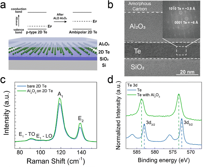 |
| | Fig. 1 (a) Schematic of the Al2O3 on 2D Te. (b) HRTEM cross-sectional image of 2D Te on Si/SiO2 substrate with an Al2O3 thin film; inset: FFT pattern converted from 2D Te nanoflake. (c) Raman spectra of bare 2D Te and Al2O3 on 2D Te. The Raman intensity corresponds to the A1, E1, and E2 modes. (d) Te 3d XPS spectra of the bare 2D Te and Al2O3 on 2D Te. | |
To investigate the effect of the Al2O3 passivation layer, the differences between the 2D Te and 2D Te with Al2O3 were analyzed by conducting Raman spectroscopy and X-ray photoelectron spectroscopy (XPS) measurements (Fig. 1c and d). Fig. 1c shows the four main Raman-active modes of the synthetic atomic layer Te measured before (blue) and after (green) Al2O3 deposition under 532 nm laser excitation. The four vibrational modes located at 90.8, 103.0, 119.2, and 139.0 cm−1 correspond to the E1-TO (E1 transverse (TO) phonon mode), E1-LO (E1 longitudinal (LO) phonon mode), A1, and E2 peaks of bare 2D Te.38 The broad E1 LO peak observed in the ∼10 nm-thick 2D Te is attributed to the deformation potential in the 2D Te lattice. In contrast, a slight red shift (∼0.2 eV) in the Raman spectra was observed following Al2O3 deposition. This indicated a weakened Raman vibration owing to the increase in electron concentration caused by the n-doping effect at the Te interface following Al2O3 deposition.47,49 A similar trend in peak shifts in the Raman spectra after Al2O3 deposition was reported in previous studies on 2D transition metal dichalcogenides (TMDCs).50–53 The uniform Raman spectrum distribution before and after Al2O3 passivation in the Raman mapping images indicated that the synthesized Te flakes exhibited consistent crystal quality across all regions and that Al2O3 was uniformly deposited on the entire Te surface (Fig. S4, ESI†).
The atomic-layered Te before (blue) and after (green) Al2O3 deposition was subjected to XPS analysis to investigate the n-doping effect induced by Al2O3 encapsulation, as shown in Fig. 1d. The Te 3d XPS analysis exhibited peaks at 582.9 and 572.5 eV, corresponding to the 3d3/2 and 3d5/2 spin–orbital doublets of the Te–Te bonds, respectively.54 Following Al2O3 deposition, the peaks shifted by 0.7 eV towards higher binding energy. Because the binding energy in the XPS spectrum is determined by the energy position of the Fermi level of the material, the shift in the peak position to a higher binding energy clearly indicated that the Fermi level of 2D Te moved towards the conduction band owing to Al2O3 deposition.55,56 Furthermore, the O/Al ratio of the Al2O3 film deposited via ALD was 1:1.45, indicating the presence of oxygen vacancies at the Al2O3 and 2D Te interface (Fig. S5 and Table S1, ESI†). The Al2O3 film deposited via ALD provides oxygen vacancies near the interface, and electronic charge transfer through these oxygen vacancies can be utilized to modulate the charge carrier polarity in 2D materials.52,57 In addition, the dissociated methyl groups from TMA as an Al precursor during ALD can transfer electrons, which contributes to the increasing electron concentration in Te.42,57 Moreover, the TMA precursor acts as a reducing agent that removes oxygen from the Te film, leading to a decrease in the Te4+ 3d3/2 and 3d5/2 peaks associated with Te–O bonds after Al2O3 thin film deposition, which suggests a decrease in the p-doping effect caused by the interaction between oxygen and Te during the synthesis process.47,58 Therefore, we confirmed that the deposition of a thin Al2O3 film on bare Te via ALD enhanced the n-type characteristics of 2D Te.
Fig. 2a illustrates the schematic of this study, where 2D Te-based artificial synaptic transistors, composed of a top gate, an Al2O3 layer deposited by ALD, and an ambipolar 2D Te semiconductor channel, serve as the foundation for logic-in-memory architecture (Fig. S6, ESI†). By modulating the Fermi level of the Te film through the deposition of the ALD Al2O3 layer, the device achieves tunable ambipolar transfer characteristics, enabling seamless switching between n-type and p-type dominant states, thus supporting desirable synaptic functions in both n- and p-type FETs (Fig. S7, ESI†). Additionally, a single 2D Te flake-based FET architecture can be configured to construct a reconfigurable inverter circuit, which can be scaled into various logic-in-memory functions by integrating multiple non-volatile FETs with stateful logic function. These features provide a straightforward pathway to realize beyond von Neumann computing with neuromorphic and logic-in-memory functions, which will be discussed in detail.
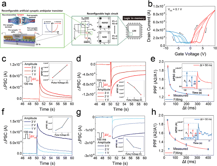 |
| | Fig. 2 (a) Schematic of the 2D Te-based synaptic ambipolar transistor, enabling reconfigurable logic circuits and integration into logic-in-memory systems. Short-term synaptic plasticity of an ambipolar 2D Te synaptic transistor. (b) IDS–VGS double-sweeping curves of the ambipolar 2D Te transistor measured at different VGS ranges under VDS = 0.1 V. N-type synaptic characteristics of (c) EPSC and (d) IPSC characteristics under different amplitudes of 1, 2, and 3 V (read voltage: 0.1 V, time duration: 100 ms); inset: EPSC and IPSC change curves under different pulses. (e) PPF index with different time intervals with VGS of 2 V for 50 ms (read voltage: 0.1 V); inset: EPSC curve triggered by a pair of presynaptic spikes with interval. P-type synaptic characteristics of (f) EPSC and (g) IPSC characteristics under different amplitudes of 1, 2, and 3 V (read voltage: 0.1 V, time duration: 100 ms); inset: EPSC and IPSC change curves under different pulses. (h) PPF index with different time intervals with VGS of 2 V for 50 ms (read voltage: 0.1 V); inset: EPSC curve triggered by a pair of presynaptic spikes with interval. | |
Biological synapses determine the synaptic weights as a function of input-spiking signals and transmit information between neurons, thereby enabling human learning and memory. Therefore, the implementation of synaptic plasticity, which changes the response of conductivity states to input stimuli, is a key capability of artificial synaptic devices. We reconfigured the gate and drain electrodes of the ambipolar FET as presynaptic and postsynaptic neurons, respectively, to mimic the learning and memory mechanisms of biological synapses. As shown in Fig. 2b, clockwise and anticlockwise hysteresis were observed for the n-FET and p-FET, respectively, which were attributed to carrier trapping/de-trapping at the trap sites of the Te/Al2O3 interface. When the gate was swept with a positive bias, the electron trap occupancy increased, causing the VTH of n-FET (p-FET) to shift positively (negatively). Consequently, the channel conductance decreased (increased) for the same gate bias. In addition, the gate-controlled electronic transfer characteristics, which exhibited a widening hysteresis window with an increase in ΔVGS, provided strong evidence for the existence of programmable multilevel conductance states in ambipolar 2D Te transistors for artificial synaptic behavior. Thus, the results clearly verify that ambipolar 2D Te transistors constructed with gate-bias controllability are potentially essential building blocks for CMOS-integrable and reconfigurable artificial synaptic devices. The short-term synaptic plasticity of the ambipolar Te artificial synaptic device was investigated by exploring the excitatory and inhibitory postsynaptic current (EPSC and IPSC) characteristics, as shown in Fig. 2c–h. The PSC characteristics of the n-FET (Fig. 2c–e) and p-FET (Fig. 2f–h) in an ambipolar FET were observed by positive and negative presynaptic electrical spiking of the gate voltage with different pulse amplitudes and durations. Fig. 2c and d shows the EPSC and IPSC response characteristics upon top-gate biasing (VGS) at 1, 2, and 3 V. EPSC corresponds to a transient current increase triggered by a positive presynaptic stimulus, emulating excitatory neural signaling, while IPSC represents a transient current suppression under a negative input, mimicking inhibitory behavior. The pulse duration and reading drain voltage (VDS) were 100 ms and 0.1 V, respectively. This indicated that PSC values increased with increasing bias amplitude. To further systematize the short-term synaptic plasticity characteristics of the ambipolar synapse device, we evaluated paired-pulse facilitation (PPF), which quantifies the enhancement of the second postsynaptic current in response to two closely spaced input pulses. Fig. 2e represents the PPF characteristics of n-FET, where PPF is defined as the ratio of the first and second PSC spikes with pulse interval time (Δt), as shown in the inset. As observed in biological synapses, the synapse weight gradually weakened as the interval time increased. The PPF decay was estimated by a double exponential decay function:59
| |  | (1) |
where
C1 and
C2 are the fast- and slow-component facilitation magnitudes, respectively; Δ
t represents the time interval between electrical spikes; and
τ1 and
τ2 are the relaxation time constants associated with the fast- and slow-term relaxation phases, respectively. The
τ1 and
τ2 values extracted from the ambipolar artificial synapse were (10.8 ms, 158.2 ms) for n-FET. In the case of the p-FET, the PSC values were also enhanced by increasing the pulse amplitude from 1 to 3 V (
Fig. 2f and g). The PPF characteristics in the p-FET showed
τ1 and
τ2 values of (12.37 ms, 115.97 ms), as indicated in
Fig. 2h. These values for both polarities were very similar to the relaxation time constants (40 ms, 300 ms) of biological synapses.
60 Further, Fig. S8 (ESI
†) shows the EPSC and IPSC characteristics as a function of various
VGS pulse durations and
VDS for both polarities, and the PSC increases with increasing pulse duration and
VDS in both n-FETs and p-FETs. Thus, the p- and n-type synaptic plasticity of the ambipolar Te artificial synapse can be governed by the gate pulse amplitude, duration, and
VDS, reflecting an outstanding replication of the biological synaptic nature.
In addition, because power consumption is an important indicator for edge computing systems, the power consumption per pulse was evaluated as follows:61
| | | Econsumption = VDS × Ipeak × tpulse | (2) |
where
VDS,
Ipeak, and
tpulse denote the reading drain voltage, EPSC peak current, and pulse width, respectively. Further, the energy consumption per single pulse for a
VDS of 1 mV,
VGS of 3 V, and duration of 100 ms was 3.5 and 19 fJ for the n-FET and p-FET, respectively (Fig. S8, ESI
†). This confirmed that the ambipolar Te artificial synapse exhibited extremely low power consumption compared to other previously reported bipolar 2D synapse devices. This proves its potential for realizing energy-efficient neuromorphic computing.
62 Furthermore, considering that the synaptic architecture of the human brain consumed approximately 10 fJ per pulse, the ambipolar Te artificial synapse transistors exhibited energy-efficient emulation of the biological synapse mechanism and were suitable for neuromorphic computing.
63
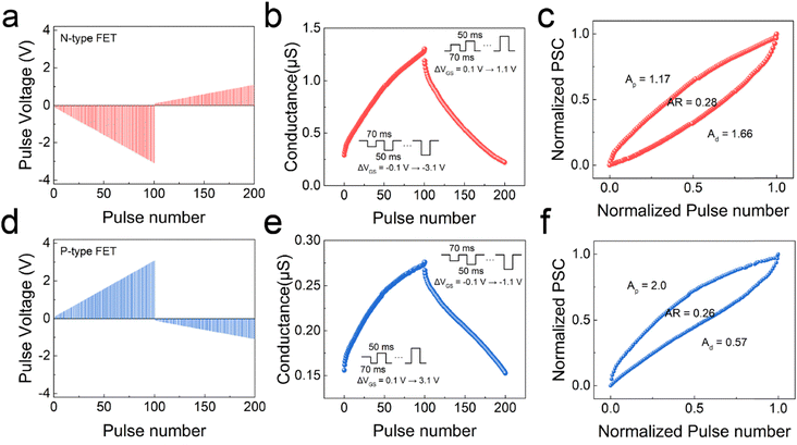
To investigate the long-term synaptic plasticity, the long-term potentiation (LTP) and depression (LTD) characteristics were analyzed by changing the conductivity under stepwise electrical gate pulse stimulation (Fig. 3). Fig. 3a–f illustrate the long-term synaptic plasticity observed in the n-FET and p-FET behaviors of the ambipolar FET, respectively. In this context, LTP and LTD refer to the gradual increase and decrease in the channel conductance over repeated pulse stimulations, emulating biological learning and forgetting. The n-FET was pulsed by gradually decreasing in steps of 30 mV from −0.1 V to −3.1 V for potentiation and increasing in steps of 10 mV from 0.1 V to 1.1 V for depression (Fig. 3a). A pulse width of 50 ms and interval time of 70 ms were applied for both the potentiation and depression. Fig. 3b shows the LTP/LTD under 100 consecutive potentiation and depression obtained by varying the presynaptic biases of the n-type FET. The gate tunability of the learning curve affected the multi-level state, dynamic range, nonlinearity (NL), and symmetry, determining the recognition accuracy of an artificial neural network (ANN).64,65 High-density multi-level states enhance the learning ability and robustness of the synapse mechanism. Further, the dynamic range, defined as the ratio of the maximum conductance (Gmax) to the minimum conductance (Gmin), significantly affects the power consumption and mapping capability of the synaptic device.66 Here, various parameters of the ambipolar artificial synapse transistor were evaluated using the following equations to assess the neural computing performance:67
| | | GLTP = B(1 − exp(−A × P)) + Gmin | (3) |
| | | GLTD = −B{1 − exp(A ×(P − Pmax))} + Gmax | (4) |
| |  | (5) |
| |  | (6) |
where
GLTP and
GLTD are the conductance values of potentiation and depression, respectively;
P and
Pmax represent the number of pulses and maximum number of pulses, respectively;
Gmax and
Gmin are the maximum and minimum conductance values, respectively;
AP,D indicates the NL value (denoted as “
A” in
eqn (3) and (4)) for potentiation (“
p”) or depression (“
d”), which determines the steepness of the conductance response curve and was extracted
via curve fitting of the experimental data; and
B denotes a fitting constant; and
n denotes the number of pulses applied during the potentiation and depression processes. For the n-type artificial synaptic transistor, the asymmetry ratio (AR) value was 0.28, and the dynamic range (
Gmax/
Gmin) was 4.49 (
Fig. 3c). In addition, the effective conductance states that represent the entire conductance variation (Δ
G =
Gmax −
Gmin) above a threshold of 0.5% were 100. The LTP/LTD characteristics of the p-FET were similar to those in the n-FET. The p-FET was pulsed in a manner opposite to that of the n-FET, with gradual increases in steps of 30 mV from 0.1 V to 3.1 V for potentiation and decreases in steps of 10 mV from 0.1 V to 1.1 V for depression (
Fig. 3d).
Fig. 3e shows the potentiation and depression characteristics of the p-FET according to the programmed pulses, and
Fig. 3f shows the resulting AR values. Using the equations to evaluate the neural computing performance, the p-type synaptic transistor obtained the AR value of 0.26, the dynamic range of 1.77, and 83 effective conductance states. It exhibited excellent characteristics for both polarities. The overall characteristics of the ambipolar Te artificial synaptic device are summarized in Table S2 (ESI
†). The device performance was comparable or superior to those of previously reported unipolar artificial synapse devices, thereby highlighting the advantages of the ambipolar Te synaptic device (Table S3, ESI
†). The gate potential profiles for the p/n-type Te synaptic FET effectively modulated the overall shapes of the LTP and LTD for each p-FET and n-FET, demonstrating excellent flexibility and reconfigurability in both online and offline learning behaviors for neuromorphic edge-computing hardware. Additionally, the reconfigurable nature and exceptional non-volatility of the ambipolar Te transistors rendered them highly suitable for simultaneously implementing neuromorphic and in-memory computing functions.
 |
| | Fig. 3 Controllability of LTP/LTD characteristics for different pulse patterns under a read voltage of 0.1 V. (a)–(c) N-type LTP/LTD characteristic curves under potentiation pulses with a gradual increase in VGS from −0.1 to −3.1 V (30 mV step) and depression pulses with a gradual decrease in VGS from 0.1 to 1.1 V (10 mV step). (d)–(f) P-type LTP/LTD characteristic curves under potentiation pulses with a gradual increase in VGS from 0.1 to 3.1 V (30 mV step) and depression pulses with a gradual decrease in VGS from −0.1 to −1.1 V (10 mV step). | |
Fig. 4a demonstrates the excellent repeatability and stability of the device, showing 10 cycles of LTP/LTD under optimal pulse conditions. Both p-type and n-type FETs exhibited low variation between cycles, thereby confirming the modulation of electrical conductivity with gradual changes in the input voltage. This indicates the excellent electrical endurance and synaptic weight adjustment ability of the Te artificial synapse transistor. Based on the 10 cycles of the LTP/LTD curves, the theoretical learning and recognition performances of the ambipolar artificial synapse transistor were investigated. To conduct the simulation, an ANN network of a two-layer multilayer perceptron neural network with 784 input neurons, 300 hidden neurons, and 10 output neurons with a back-propagation algorithm architecture was configured, as shown in Fig. 4b. The 784 input neurons of the ANN corresponded to the handwritten digits of the 28 × 28 pixel2 MNIST dataset image, and the 10 output neurons corresponded to the numbers 0–9. Fig. 4c shows the pattern recognition accuracy of the artificial synapses in the p-FET and n-FET as a function of the number of training epochs. The recognition accuracy of both the FETs instantly exceeded 90% during the first training epoch. Following 40 training epochs, high recognition accuracy of 94.7% and 94.2% were achieved for the p-FET and n-FET, respectively. The ideal recognition accuracy is 97.8%. Therefore, the high-quality Te ambipolar FET operating in bipolarity, including its excellent electrical durability and high pattern recognition accuracy, ensured robustness and efficiency for energy-efficient and CMOS-integrable neuromorphic and logic-in-memory architectures with memory and learning functions, thereby demonstrating significant potential in these applications.
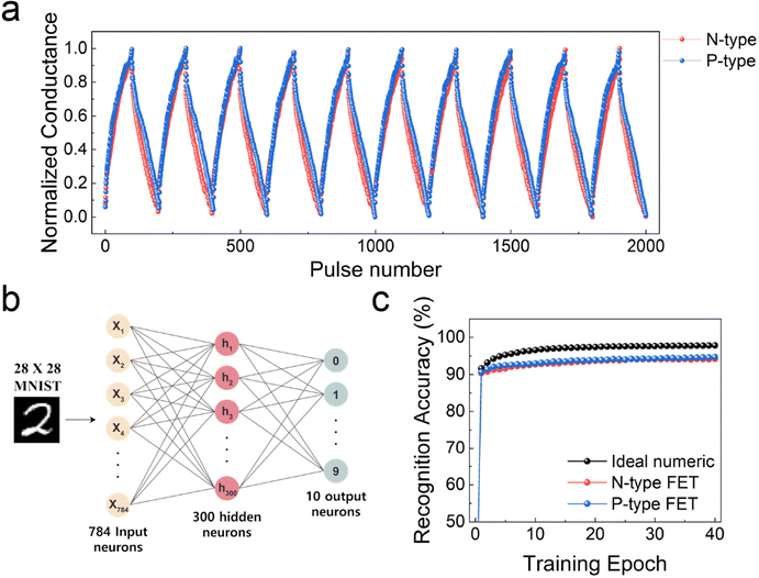 |
| | Fig. 4 (a) Endurance characteristics of the ambipolar synaptic device for 10 cycles reacting under different gate pulse bases. (b) Schematic of a two-layer multilayer perceptron neural network on the MNIST 28 × 28 pixels handwritten digits data set. (c) Simulated recognition accuracy based on MNIST dataset comparisons for p-type and n-type FET. | |
To demonstrate the potential of the ambipolar Te transistor as a logic device, we fabricated a CMOS inverter using a single 2D Te flake (Fig. 5). Fig. 5a shows the schematic and circuit diagram of the inverter fabricated by the serial connection of ambipolar transistors capped with Al2O3 thin film on single Te flakes. The operating principle of the inverter can be briefly explained using the band diagram in Fig. 5b. An applied VDD of +10 V to the source of transistor 1 (Tr1) was equivalent to the application of a gate bias of −10 V. However, as transistor 2 (Tr2) was connected to the ground, there was no voltage difference with the gate. Therefore, when Vin was within −10 V and 0 V, holes in Tr1 could move from the source to the drain, rendering the hole current dominant in Tr1. In other words, Tr1 was in the ON state (p-type) and Tr2 was in the OFF state with Vout = 10 V. When Vin was between 0–10 V, the electrons in Tr2 could move from the source to the drain, rendering the electron current dominant in Tr2. Consequently, Tr1 was in the OFF state and Tr2 was in the ON state (n-type), resulting in Vout = 0 V. By controlling the polarity and magnitude of Vin and VDD, p-/n-channel transistors can be determined, facilitating the easy fabrication of an inverter device within a single 2D Te flake.68,69 The voltage transfer characteristics (VTC) measured at various VDD values demonstrated the NOT logic gate function, as shown in Fig. 5c. When VDD was applied at 5, 7, and 10 V, the inverter switched to 0 V at a specific VDD. This distinct switching effect in a single Te flake inverter composed of 2D ambipolar Te transistors was clearly observed, which is indicative of typical CMOS inverter characteristics. The VTCs in the ambipolar Te inverter were comparable to those reported in previous studies using 2D heterostructured-inverters.70–72Fig. 5d shows the voltage gain in response to the input voltage for each VDD value. The full-swing output operation feature in the ambipolar-based inverter, coupled with good conducting symmetry, resulted in a clear gain value of approximately 1.7 at a maximal VDD (10 V). This indicated a relatively good amplification capability of the input signal. Furthermore, the retention characteristics of the transistor could be regulated by modulating the gate bias range to enable fast switching, as shown in Fig. S9 (ESI†). This indicates that a CMOS inverter with a single ambipolar Te device configuration offers a flexible, efficient, and compact circuit design to achieve 2D nanomaterial-based CMOS-integrable logic circuitry without additional complicated fabrication processes.
 |
| | Fig. 5 (a) Schematic of the inverter device with ambipolar 2D Te/Al2O3. (b) Band diagrams of two ambipolar transistors at different states (VDD = 10 V) (c) Voltage transfer characteristics of the CMOS inverter at VDD = 5, 7, and 10 V. (d) Voltage gain of the CMOS inverter at VDD = 5, 7, and 10 V. | |
Next, we verified the capability of logic-in-memory computing based on ambipolar Te transistors by simulating the logic-in-memory circuits as a function of pre-programmed input signals based on an ambipolar Te inverter and transfer characteristics using a PSpice simulator (Cadence) (Fig. 6). Fig. 6a shows the logic diagram and truth table of the programmable inverter designed using an ambipolar Te FET. The transistors operated as either p-FET or n-FET based on pre-programmed input signals with an equivalent magnitude but opposite polarity in their electrical characteristics (Pre-Sin,P1, Pre-Sin,P2). Here, the Vout value was determined by the Vin value, and the pre-programmed memory state (Q) could be observed. Upon executing the preprogramming signals, the circuit effectively maintained the conducting states owing to the outstanding synaptic plasticity of the ambipolar Te, allowing the half-recording of the logic results to be embedded within its structure. Subsequently, the VTCs uncovered past information, thereby revealing the memory states of the circuit (Q). For example, with the input signals Pre-Sin,P1 = “1” and Pre-Sin,P2 = “0”, if Vin = “1”, the resulting Vout will be “0”, allowing it to function as an inverter. Following operation, the pre-input signal corresponding to Q = “1” was stored. This context weaved the framework of logic-in-memory computing. In this way, various logic gates, such as NAND, NOR XOR, and XNOR, can be easily constructed by combining multiple Te ambipolar FETs. Simple two-input logic gate circuits are shown in Fig. 6b, where the FETs receiving the same pre-programmed input signal are grouped and labeled as P1 and P2. Using pre-programmed input signals, NAND, NOR, XOR, and XNOR circuits were designed and reconfigured by controlling Pre-Sin,P1, Pre-Sin,P2, and VDD/GND. For example, to activate the NAND (NOR) logic circuit, a pair of signals, Pre-Sin,P1 = “1” (“0”) and Pre-Sin,P2 = “0” (“1”), was used. In this design, VDD (or GND) was connected to parallel P 1s, whereas GND (or VDD) was connected to series P 2s. Similarly, XOR and XNOR circuits were reconfigured in this manner. Fig. 6c illustrates the operational results for these logic gates, showing the output for all four input combinations (“00”, “01”, “10”, “11”). The results indicated the effective implementation of reconfigurable logic gates for logic-in-memory computing. Thus, ambipolar Te synaptic transistors with CMOS-integrable and reconfigurable natures can provide a groundbreaking platform for next-generation in-memory computations.
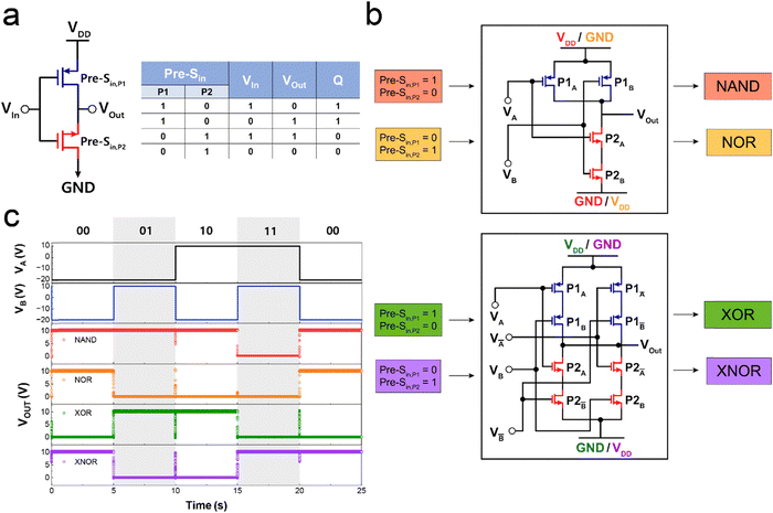 |
| | Fig. 6 (a) Schematic of the pre-programmable 2D ambipolar Te inverter (left) and the programmable inverter truth table (right). (b) Circuit diagram of the reconfigurable two-input logic gate circuits based on ambipolar 2D Te FET, illustrating functionality as NAND, NOR, XOR, and XNOR gates depending on the pre-programmed input signals. (c) Simulated waveforms operating in various logic gate circuits (Vin amplitude: 30 V). | |
Conclusion
This study constructed an efficient logic-in-memory architecture based on an artificial synaptic device using 2D Te with an Al2O3 thin film. By adopting a carrier concentration control method that precisely controlled the thickness while minimizing channel damage through the ALD system, an ambipolar Te FET was fabricated. The artificial synapse memory device utilizing ambipolar FET demonstrated ultra-low power consumption (3.5 and 19 fJ for n-type and p-type, respectively) and exhibited excellent short- and long-term synaptic plasticity. Based on the LTP/LTD characteristics with high linearity and symmetry, the synaptic device achieved a high recognition accuracy in the MNIST pattern recognition simulation of 94.7% and 94.2% for p-type and n-type, respectively. These results confirmed the successful emulation of biological neuromorphic systems and indicated their suitability for reconfigurable in-memory computing hardware. In addition, the demonstration of a NOT logic gate implemented by modulating the voltage bias without doping using a single Te flake passivated with Al2O3, along with the simulation of various logic circuits in memory, indicated superior circuit design flexibility and efficiency compared with conventional CMOS technology. Consequently, this study represents a significant step beyond von Neumann architecture by presenting a logic-in-memory device and a neuromorphic computing based on ambipolar artificial synapses within a one-transistor structure.
Author contributions
B. You and J. Huh designed the experiments, analyzed the data, performed the experiments, interpreted the results, and wrote the manuscript. Y. Kim performed the experiments. M. Y. analyzed the data. U. Kim, M. K. Joo, and M. G. Hahm supervised the study. M. Lee designed the experiments, wrote the manuscript, and supervised the project.
Data availability
The data that support the findings of this study are available from the corresponding author upon reasonable request.
Conflicts of interest
The authors declare no competing financial interests.
Acknowledgements
This work was supported by the National Research Foundation of Korea (NRF) grant funded by the Korea government (MSIT) (RS-2024-00454415, RS-2025-00514053, RS-2024-00412554, RS-2023-00254934 (M.-K. J.))
References
- M. Hilbert and P. López, Science, 2011, 332, 60–65 CrossRef CAS PubMed.
- Y. Taur, D. A. Buchanan, W. Chen, D. J. Frank, K. E. Ismail, S.-H. Lo, G. A. Sai-Halasz, R. G. Viswanathan, H.-J. Wann and S. J. Wind, Proc. IEEE, 1997, 85, 486–504 Search PubMed.
- T. Bohnstingl, F. Scherr, C. Pehle, K. Meier and W. Maass, Front. Neurosci., 2019, 13, 483 Search PubMed.
- G. W. Burr, R. M. Shelby, A. Sebastian, S. Kim, S. Kim, S. Sidler, K. Virwani, M. Ishii, P. Narayanan and A. Fumarola, Adv. Phys.: X, 2017, 2, 89–124 Search PubMed.
- E. Painkras, L. A. Plana, J. Garside, S. Temple, F. Galluppi, C. Patterson, D. R. Lester, A. D. Brown and S. B. Furber, IEEE, J. Solid State Circ., 2013, 48, 1943–1953 Search PubMed.
- A. Sebastian, M. Le Gallo, R. Khaddam-Aljameh and E. Eleftheriou, Nat. Nanotechnol., 2020, 15, 529–544 Search PubMed.
- D. Ielmini and H.-S. P. Wong, Nat. Electr., 2018, 1, 333–343 Search PubMed.
- M. Chaudhary, T. Y. Yang, C. T. Chen, P. C. Lai, Y. C. Hsu, Y. R. Peng, A. Kumar, C. H. Lee and Y. L. Chueh, Adv. Funct. Mater., 2023, 33, 2303697 Search PubMed.
- I. Boybat, M. Le Gallo, S. Nandakumar, T. Moraitis, T. Parnell, T. Tuma, B. Rajendran, Y. Leblebici, A. Sebastian and E. Eleftheriou, Nat. Commun., 2018, 9, 2514 Search PubMed.
- L. Q. Zhu, C. J. Wan, L. Q. Guo, Y. Shi and Q. Wan, Nat. Commun., 2014, 5, 3158 Search PubMed.
- P. A. Merolla, J. V. Arthur, R. Alvarez-Icaza, A. S. Cassidy, J. Sawada, F. Akopyan, B. L. Jackson, N. Imam, C. Guo and Y. Nakamura, Science, 2014, 345, 668–673 Search PubMed.
- G. Indiveri and S.-C. Liu, Proc. IEEE, 2015, 103, 1379–1397 Search PubMed.
- D. S. Jeong, K. M. Kim, S. Kim, B. J. Choi and C. S. Hwang, Adv. Electron. Mater., 2016, 2, 1600090 Search PubMed.
- J. Bae, J. Won and W. Shim, Nano Energy, 2024, 109646 Search PubMed.
- Y. Zhang, Z. Wang, J. Zhu, Y. Yang, M. Rao, W. Song, Y. Zhuo, X. Zhang, M. Cui and L. Shen, Appl. Phys. Rev., 2020, 7, 011308 Search PubMed.
- S. H. Jo, T. Chang, I. Ebong, B. B. Bhadviya, P. Mazumder and W. Lu, Nano Lett., 2010, 10, 1297–1301 Search PubMed.
- Z. Lv, Y. Wang, J. Chen, J. Wang, Y. Zhou and S.-T. Han, Chem. Rev., 2020, 120, 3941–4006 Search PubMed.
- Z. Lv, M. Chen, F. Qian, V. A. Roy, W. Ye, D. She, Y. Wang, Z. X. Xu, Y. Zhou and S. T. Han, Adv. Funct. Mater., 2019, 29, 1902374 Search PubMed.
- Y. N. Zhong, T. Wang, X. Gao, J. L. Xu and S. D. Wang, Adv. Funct. Mater., 2018, 28, 1800854 Search PubMed.
- H. Ling, M. Yi, M. Nagai, L. Xie, L. Wang, B. Hu and W. Huang, Adv. Mater., 2017, 29, 1701333 Search PubMed.
- F. Ma, Y. Zhu, Z. Xu, Y. Liu, X. Zheng, S. Ju, Q. Li, Z. Ni, H. Hu and Y. Chai, Adv. Funct. Mater., 2020, 30, 1908901 Search PubMed.
- R. A. John, N. Yantara, S. E. Ng, M. I. B. Patdillah, M. R. Kulkarni, N. F. Jamaludin, J. Basu, N. Ankit, S. G. Mhaisalkar and A. Basu, Adv. Mater., 2021, 33, 2007851 Search PubMed.
- M. Lee, W. Lee, S. Choi, J. W. Jo, J. Kim, S. K. Park and Y. H. Kim, Adv. Mater., 2017, 29, 1700951 Search PubMed.
- C. J. Wan, Y. H. Liu, P. Feng, W. Wang, L. Q. Zhu, Z. P. Liu, Y. Shi and Q. Wan, Adv. Mater., 2016, 28, 5878–5885 Search PubMed.
- C. J. Wan, Y. H. Liu, L. Q. Zhu, P. Feng, Y. Shi and Q. Wan, ACS Appl. Mater. Interfaces, 2016, 8, 9762–9768 Search PubMed.
- A. J. Arnold, A. Razavieh, J. R. Nasr, D. S. Schulman, C. M. Eichfeld and S. Das, ACS Nano, 2017, 11, 3110–3118 CrossRef CAS PubMed.
- Z. Zhang, S. Wang, C. Liu, R. Xie, W. Hu and P. Zhou, Nat. Nanotechnol., 2022, 17, 27–32 Search PubMed.
- L. Mennel, J. Symonowicz, S. Wachter, D. K. Polyushkin, A. J. Molina-Mendoza and T. Mueller, Nature, 2020, 579, 62–66 Search PubMed.
- K. C. Kwon, J. H. Baek, K. Hong, S. Y. Kim and H. W. Jang, Nano-Micro Lett., 2022, 14, 58 Search PubMed.
- X. Hou, C. Liu, Y. Ding, L. Liu, S. Wang and P. Zhou, Adv. Sci., 2020, 7, 2002072 Search PubMed.
- Y. Shi, X. Liang, B. Yuan, V. Chen, H. Li, F. Hui, Z. Yu, F. Yuan, E. Pop and H.-S. P. Wong, Nat. Electr., 2018, 1, 458–465 Search PubMed.
- M. Wang, S. Cai, C. Pan, C. Wang, X. Lian, Y. Zhuo, K. Xu, T. Cao, X. Pan and B. Wang, Nat. Electr., 2018, 1, 130–136 Search PubMed.
- R. Ge, X. Wu, M. Kim, J. Shi, S. Sonde, L. Tao, Y. Zhang, J. C. Lee and D. Akinwande, Nano Lett., 2018, 18, 434–441 Search PubMed.
- C. Huyghebaert, T. Schram, Q. Smets, T. K. Agarwal, D. Verreck, S. Brems, A. Phommahaxay, D. Chiappe, S. El Kazzi and C. L. De La Rosa, Proc. IEEE Int. Electron Devices Meet., 2018, 2018, 22.1–22.4 Search PubMed.
- G. Migliato Marega, Y. Zhao, A. Avsar, Z. Wang, M. Tripathi, A. Radenovic and A. Kis, Nature, 2020, 587, 72–77 Search PubMed.
- M.-P. Lee, C. Gao, M.-Y. Tsai, C.-Y. Lin, F.-S. Yang, H.-Y. Sung, C. Zhang, W. Li, J. Li and J. Zhang, Sci. Adv., 2023, 9, eadk1597 Search PubMed.
- L. Kong, X. Zhang, Q. Tao, M. Zhang, W. Dang, Z. Li, L. Feng, L. Liao, X. Duan and Y. Liu, Nat. Commun., 2020, 11, 1866 Search PubMed.
- Y. Wang, G. Qiu, R. Wang, S. Huang, Q. Wang, Y. Liu, Y. Du, W. A. Goddard III, M. J. Kim and X. Xu, Nat. Electr., 2018, 1, 228–236 Search PubMed.
- Z. Shi, R. Cao, K. Khan, A. K. Tareen, X. Liu, W. Liang, Y. Zhang, C. Ma, Z. Guo and X. Luo, Nano-Micro Lett., 2020, 12, 1–34 Search PubMed.
- C. Zhao, C. Tan, D.-H. Lien, X. Song, M. Amani, M. Hettick, H. Y. Y. Nyein, Z. Yuan, L. Li and M. C. Scott, Nat. Nanotechnol., 2020, 15, 53–58 Search PubMed.
- M. Amani, C. Tan, G. Zhang, C. Zhao, J. Bullock, X. Song, H. Kim, V. R. Shrestha, Y. Gao and K. B. Crozier, ACS Nano, 2018, 12, 7253–7263 Search PubMed.
- A. Leonhardt, D. Chiappe, V. V. Afanas’ ev, S. El Kazzi, I. Shlyakhov, T. Conard, A. Franquet, C. Huyghebaert and S. De Gendt, ACS Appl. Mater. Interfaces, 2019, 11, 42697–42707 Search PubMed.
- W. Zhang, S. Shrestha, S. Parajuli, B. B. Maskey, J. Park, H. Yang, Y. Jung and G. Cho, Nanoscale Adv., 2023, 5, 3879–3886 Search PubMed.
- R. L. Puurunen, J. Appl. Phys., 2005, 97, 121301 Search PubMed.
- R. W. Johnson, A. Hultqvist and S. F. Bent, Mater. Today, 2014, 17, 236–246 Search PubMed.
- B. You, J. Yoon, Y. Kim, M. Yang, J. Bak, J. Park, U. J. Kim, M. G. Hahm and M. Lee, J. Mater. Chem. C, 2024, 12, 6596–6605 Search PubMed.
- D. A. Nguyen, S. Cho, S. Park, D. Y. Park, H. C. Suh, M. S. Jeong, T. P. A. Bach, H. Kim and H. Im, Nano Energy, 2023, 113, 108552 CrossRef CAS.
- G. Qiu, A. Charnas, C. Niu, Y. Wang, W. Wu and P. D. Ye, npj 2D Mater. Appl., 2022, 6, 17 Search PubMed.
- S. Y. Kim, H. I. Yang and W. Choi, Appl. Phys. Lett., 2018, 113, 133104 Search PubMed.
- K. Chen, D. Kiriya, M. Hettick, M. Tosun, T.-J. Ha, S. R. Madhvapathy, S. Desai, A. Sachid and A. Javey, APL Mater., 2014, 2, 092504 Search PubMed.
- C. J. L. de la Rosa, A. Nourbakhsh, M. Heyne, I. Asselberghs, C. Huyghebaert, I. Radu, M. Heyns and S. De Gendt, Nanoscale, 2017, 9, 258–265 Search PubMed.
- Y. J. Park, A. K. Katiyar, A. T. Hoang and J. H. Ahn, Small, 2019, 15, 1901772 Search PubMed.
- T. Das, S. Youn, J. E. Seo, E. Yang and J. Chang, ACS Appl. Mater. Interfaces, 2023, 15, 45116–45127 CrossRef CAS PubMed.
- J. Yoon, B. You, Y. Kim, J. Bak, M. Yang, J. Park, M. G. Hahm and M. Lee, ACS Appl. Mater. Interfaces, 2023, 15, 18463–18472 CrossRef CAS PubMed.
- M. Li, D. Gao, S. Li, Z. Zhou, J. Zou, H. Tao, L. Wang, M. Xu and J. Peng, RSC Adv., 2015, 5, 104613 RSC.
- C. Guerra-Nuñez, M. Döbeli, J. Michler and I. Utke, Chem. Mater., 2017, 29, 8690–8703 Search PubMed.
- A. Valsaraj, J. Chang, A. Rai, L. F. Register and S. K. Banerjee, 2D Mater., 2015, 2, 045009 CrossRef.
- T. Kim, C. H. Choi, P. Byeon, M. Lee, A. Song, K.-B. Chung, S. Han, S.-Y. Chung, K.-S. Park and J. K. Jeong, npj 2D Mater. Appl., 2022, 6, 4 Search PubMed.
- S. G. Hu, Y. Liu, T. P. Chen, Z. Liu, Q. Yu, L. J. Deng, Y. Yin and S. Hosaka, Appl. Phys. Lett., 2013, 102, 183510 Search PubMed.
- R. S. Zucker and W. G. Regehr, Annu. Rev. Physiol., 2002, 64, 355–405 Search PubMed.
- C.-H. Huang, Y. Zhang and K. Nomura, ACS Appl. Mater. Interfaces, 2022, 14, 22252–22262 Search PubMed.
- C. Yao, G. Wu, M. Huang, W. Wang, C. Zhang, J. Wu, H. Liu, B. Zheng, J. Yi and C. Zhu, ACS Appl. Mater. Interfaces, 2023, 15, 23573–23582 CrossRef CAS PubMed.
- H. L. Park, Y. Lee, N. Kim, D. G. Seo, G. T. Go and T. W. Lee, Adv. Mater., 2020, 32, 1903558 Search PubMed.
- M.-K. Kim and J.-S. Lee, Nano Lett., 2019, 19, 2044–2050 CrossRef CAS PubMed.
- Y. Li, J. Lu, D. Shang, Q. Liu, S. Wu, Z. Wu, X. Zhang, J. Yang, Z. Wang and H. Lv, Adv. Mater., 2020, 32, 2003018 CrossRef CAS PubMed.
- K. C. Kwon, Y. Zhang, L. Wang, W. Yu, X. Wang, I.-H. Park, H. S. Choi, T. Ma, Z. Zhu and B. Tian, ACS Nano, 2020, 14, 7628–7638 CrossRef CAS PubMed.
- C. Wang, Y. Li, Y. Wang, X. Xu, M. Fu, Y. Liu, Z. Lin, H. Ling, P. Gkoupidenis and M. Yi, J. Mater. Chem. C, 2021, 9, 11464–11483 Search PubMed.
- W. J. Yu, U. J. Kim, B. R. Kang, I. H. Lee, E.-H. Lee and Y. H. Lee, Nano Lett., 2009, 9, 1401–1405 Search PubMed.
- Y.-M. Chang, S.-H. Yang, C.-Y. Lin, C.-H. Chen, C.-H. Lien, W.-B. Jian, K. Ueno, Y.-W. Suen, K. Tsukagoshi and Y.-F. Lin, Adv. Mater., 2018, 30, 1706995 Search PubMed.
- X. Chen, H. Chen, Y. Sun, S. Zhang, Y. Xia, D. W. Zhang, P. Zhou, W. Li, Z. Sun and W. Bao, 2D Mater., 2022, 9, 035015 Search PubMed.
- Y. Su, C. U. Kshirsagar, M. C. Robbins, N. Haratipour and S. J. Koester, 2D Mater., 2016, 3, 011006 CrossRef.
- X. He, W. Chow, F. Liu, B. Tay and Z. Liu, Small, 2017, 13, 1602558 Search PubMed.
Footnotes |
| † Electronic supplementary information (ESI) available: Detailed material preparation and device fabrication, hydrothermal synthesizing process of Te, the thickness of Te with AFM image, HRTEM cross-section image of synaptic device, Raman and XPS spectra of Te/Al2O3, atomic percentage in 2D Te flake with Al2O3, I–V curve of ambipolar Te FET, short-term synaptic plasticity characteristics, retention characteristics, summarize of gate tunability performance and performance comparison with previously report, double exponential decay equation, estimation of power consumption, estimation of parameters to assess the neural computing performance (PDF). See DOI: https://doi.org/10.1039/d5nh00113g |
| ‡ Bolim You and Jihoon Huh contributed equally to this paper. |
|
| This journal is © The Royal Society of Chemistry 2025 |
Click here to see how this site uses Cookies. View our privacy policy here. 
 *ab
*ab


