DOI:
10.1039/D5NH00228A
(Communication)
Nanoscale Horiz., 2025,
10, 1345-1353
High electrical conductivity in directionally polymerized C60 nanowires by grazing incidence of single particles†
Received
11th April 2025
, Accepted 19th May 2025
First published on 20th May 2025
Abstract
As organic electronics continue to evolve, there is a growing demand for nanometer-scale microfabrication techniques for organic semiconductors. Although precise 2D alignment and 3D integration are essential for future device applications, significant challenges remain, particularly with organic materials. Here, we demonstrate the successful fabrication of highly oriented nanowire arrays of fullerene (C60) via directional polymerization, mediated by grazing incidence of high-energy charged particles. These C60 nanowires exhibit remarkably high electrical conductivity, comparable to that of undoped germanium, which is attributed to a unique polymerization process induced by particle irradiation. Field-effect transistor (FET) measurements revealed that electrons serve as the primary charge carriers in the nanowires. Temperature-dependent electrical measurements further indicate that the conduction mechanism follows a thermally activated hopping process, rather than conventional band conduction, reflecting the amorphous and crosslinked nature of the polymerized nanowires. Furthermore, a measurable change in conductivity upon nitrobenzene adsorption suggests their potential application as highly sensitive, electron-based organic gas sensors.
New concepts
The new concept of this study is the directional polymerization of C60 molecules induced by grazing-incidence charged particles, which enables the fabrication of highly aligned, sub-10 nm organic nanowires with high electrical conductivity. This technique, referred to as the STLiP (single particle-triggered linear polymerization) method, utilizes high-energy charged particles to trigger the covalent bonding of C60 molecules along the particle trajectory, forming straight nanowires that are fixed onto a substrate via interfacial adhesion. Unlike conventional lithographic approaches where organic molecules are often passive structural components, this method leverages the intrinsic chemical reactivity of C60 under ionizing radiation to actively construct functional conductive paths. The resulting nanowires exhibit minimal inter-wire interaction, allowing for precise evaluation of their intrinsic electrical properties. Despite their nanoscale diameters, the nanowires retain a two- to three-dimensional conduction character and show strong anisotropic conductivity, aligned along the direction of ion irradiation. Moreover, these nanowire arrays demonstrate selective absorption of electromagnetic waves in the GHz to THz range, particularly when the electric field vector is parallel to the nanowire axis. This unique optical and electronic behavior suggests promising applications in next-generation organic electronics, including transparent and frequency-selective shielding materials or highly sensitive molecular sensors. To date, no other study has reported organic nanowires in the true sub-10 nm regime with this level of alignment and conductive performance. Thus, the concept presented here provides new directions in the design of molecular-scale functional materials and organic semiconductor devices by integrating directional polymerization, nanoscale morphology control, and advanced ion beam techniques.
|
1. Introduction
A variety of low-dimensional materials with electrical conductivity have been designed and synthesized to date, exhibiting unique conduction mechanisms unlike conventional conductors/semiconductors.1–4 To understand the precise mechanism of electrical conductivity, one-dimensional (1D) structures confined to a few nanometers serve as the simplest systems for precise conduction analysis using theoretical models. One-dimensional nanomaterials, including nanowires, nanorods, and nanofibers, have been produced based on metals, inorganic conductors/semiconductors, and conjugated organic molecules and have attracted considerable attention as critical materials not only for analysis but also for applications.5–9
Electrical conductivity in 1D nanomaterials of a single nanometer in diameter is expected to fall into the region known as quantum electrical conduction, transforming the materials into quantum wires.10,11 Quantum mechanical electric conduction has been demonstrated in nanowires composed of metals or inorganic semiconductors with exotic electronic,12–14 optical,7,15 and/or thermal16,17 devices. Organic molecular 1D nanostructures, in contrast, have not yet been elucidated, mainly because of the issues in the fabrication processes with finely controlled sizes. Condensed phases of organic molecules are generally stabilized with weak van der Waals (vdW) interactions, making it hard to assemble them into the finite position with suppressed thermal fluctuation and molecular orientation with high crystallinity.
Such nanowires are particularly important in emerging applications, including flexible electronics, nanoscale sensing, and molecular memory, where directional charge transport, nanoscale precision, and moderate conductivity are essential. In these fields, organic materials offer unique advantages, such as mechanical flexibility, lightweight, solution processability, and compatibility with soft substrates.18–23 However, achieving both high structural order and sufficient conductivity in organic nanowires remains challenging. Therefore, developing a scalable method to fabricate well-aligned, conductive organic nanowires holds significant promise for next-generation device platforms.
The strategies for aggregation of organic molecules into nanomaterials can be divided into two main categories: (i) self-assembly based on intermolecular interactions and (ii) polymerization through covalent bonds. The former strategy targets highly planar raw material molecules with π–π conjugation, and nanowires are formed by bottom–up processes, such as physical vapor-phase transport and liquid-phase self-assembly.24,25 In particular, supramolecular nanowires with a single molecule-sized diameter can be precisely controlled to achieve the desired physical properties.26 The nanostructures are, however, stabilized via weak vdW interactions, which is disadvantageous for precise control of the structural stability against thermal fluctuation and for facilitating highly conductive pathways. The latter have often been used for conjugated electronic conductive polymers as the thinnest 1D unit, mainly top–down processes, such as etching using porous anodized aluminum oxide (AAO) templates,27 lithography using photo, electron, and ion beam irradiation,28–30 and electrospinning.31 The fabrication of vertically and/or horizontally oriented nanowire arrays are a critical technology for immediate device application.
The high-density energy imparted to the irradiation target by high-energy charged particles has been used for producing organic nanowires (SPNT/STLiP).32–34 We also reported on free-standing nanowire arrays produced by vacuum heating.35 The wide range of material selection and the development of high-dimensional integration methods enabled the application of these nanowires to electronic devices. In addition, while the chemical/electronic structure of the nanowires created using this method has long been an issue, the evaluation of electrical properties allows us to gain insight into them as well as the utility of nanowire systems as practical devices. In this paper, we report on the high electrical conductivity of nanowires based on fullerene C60. C60 was chosen for the following reasons: it is entirely composed of carbon, it has perfect spherical symmetry (0D), and it has a conjugated system that extends within the molecule. In the nano-wiring (polymerization) process using high-energy charged particles, the isotropic nature of spherical C60 turns into unidirectional molecular condensates with dimensional transformation in the solid state: the target of electric conductivity measurement in this work.
2. Results and discussion
2.1. Fabrication and morphology of horizontally aligned C60 nanowire arrays
Fig. 1(a) presents a schematic illustration of the fabrication process for horizontally aligned nanowire arrays. A thin organic C60 film (up to 300 nm thick) was deposited onto a p-doped (n-type) silicon substrate using vacuum deposition. Notably, the Si substrate was coated with a 200 nm layer of thermally grown SiO2. High-energy 129Xe23+ ions (450 MeV) were irradiated onto the sample at a grazing incidence angle (θ < 3°). Due to their extremely high kinetic energy (MeV–GeV scale), these ions follow straight trajectories, which in turn facilitate the formation of straight nanowires within the thin film. Following irradiation, the substrates were rinsed with o-dichlorobenzene (ODCB) to remove unreacted C60, leaving behind only the nanowires. Fig. 1(b–d) show atomic force microscopy (AFM) images of the resulting horizontally aligned nanowire arrays. As each incident ion generates a single nanowire, the number of nanowires can be tuned by adjusting the ion fluence (f), with confirmed distributions at f = 1 × 109 cm−2, 1 × 1010 cm−2, and 1 × 1011 cm−2. The nanowires remained horizontally aligned, even after solvent exposure, despite surface tension-induced fluctuations during the isolation process. In contrast, conventional vertical irradiation methods often yield randomly oriented nanowires due to solvent-induced surface tension effects during development.35,36 The maintained alignment observed here suggests that the inherent rigidity of the C60 nanowires contributed to their structural integrity. For comparison, horizontally aligned rubrene-based nanowires fabricated under the same conditions exhibited poor alignment due to frequent entanglement and breakage (Fig. S1, ESI†). The average radius of the C60 nanowires was measured to be 4.6 ± 0.3 nm (Fig. S2, ESI†), which is significantly smaller than that of C60 nanowires produced by conventional solvent development methods.36 This reduction is likely attributed to the unique nanowire formation mechanism of the STLiP (single particle-triggered linear polymerization) process. Nanowire formation is governed by the ion track structure, composed of a dense core region and a surrounding penumbra region.32 Given that the core region typically has a radius below 1 nm, the nanowires are largely formed within the penumbra region, where energy deposition exceeds the threshold required for molecular reorganization. The energy density distribution in the penumbra region (ρp) can be expressed as follows:| |  | (1) |
where r is the distance from the center of the trajectory, and rp and rc are the core and penumbra region radii, respectively. Linear energy transfer (LET) refers to the energy added by the charged particle to the surrounding environment per unit distance traveled.37 From eqn (1), it is clear that the energy dispersion of the penumbra region relies on the LET of the particles. The Stopping and Range of Ions in Matter (SRIM) simulation (SRIM-2013) for the LET of 450 MeV 129Xe23+ to C60 revealed that the average length of the ion trajectory was about 42 μm (Fig. S3, ESI†). Based on our previous studies,35,36 it is estimated that the LET required for nanowire formation is about 8000 eV nm−1, so the C60 nanowires in this case are presumed to have reached a maximum length of about 35 μm. However, following the LET penetration depth dependence shown in Fig. S2(b) (ESI†), the radius of the nanowires would not be perfectly uniform. In other words, the nanowires become thinner as the penetration distance of the charged particles deepens, so that the C60 nanowire radius in this study is smaller on average than previously reported.
 |
| | Fig. 1 Fabrication of horizontally aligned nanowire arrays by high-energy charged particle irradiation. (a) Schematic illustration of horizontally – aligned C60 nanowire arrays via the STLiP method. (b)–(d) AFM images of horizontally aligned nanowire arrays at a fluence (f) of (b) 1 × 109 cm−2, (c) 1 × 1010 cm−2, and (d) 1 × 1011 cm−2. (e) Height profile along the red line in Fig. 1(d). | |
2.2. Electrical evaluation of horizontally aligned nanowires using FET configuration
To evaluate the electrical conduction of the horizontally aligned nanowires, a field-effect transistor (FET) device was fabricated, as illustrated in Fig. 2(a). Source–drain electrode patterns were defined via photolithography on a Si/SiO2 gate substrate onto which the aligned nanowires had been deposited. Chromium (2 nm) and gold (50 nm) were subsequently vacuum-deposited as adhesion and conduction layers, respectively. The channel length was fixed at L = 5 μm, while the channel width (W) was varied as W = 200, 500, and 1500 μm. The nanowires were aligned precisely in the direction of the channel, and L was chosen to be shorter than the nanowire lengths (>10 μm) to ensure full channel coverage. The fluence-dependent current–voltage (I–V) characteristics measured at gate voltage VG = 0 V and W = 200 μm are shown in Fig. 2(b). The observed current increased linearly with fluence, indicating that the number of nanowires bridging the source–drain electrodes governs the conduction. This linear relationship implies a uniform electrical conductivity among the nanowires fabricated by the STLiP technique. It is worth noting that the electrodes were fabricated after nanowire formation via multiple lithographic steps—development, metal deposition, and lift-off. The maintained linearity of the I–V characteristics suggests that the nanowires exhibit high structural and electrical stability throughout the post-fabrication processes. As shown in Fig. 2(c), the current at f = 1 × 1010 cm−2 also increases linearly with W, which is consistent with an increasing number of nanowires bridging the channel. This further supports both the uniform conductivity and the homogeneous spatial distribution of the isolated nanowires. Additionally, as shown in Fig. S4 (ESI†), the current at a fixed source–drain voltage (VSD) is proportional to the number of bridging nanowires. This suggests minimal influence of ion irradiation on the gate insulator beneath the nanowires and confirms that the capacitance of the FET device remained essentially unchanged.
 |
| | Fig. 2 Evaluation of electrical conductivity of horizontally aligned nanowires. (a) Illustration of nanowire FET device. VDS and VG represent the drain–source and gate voltages, respectively. W is the width of the electrodes, while L is the gap between the electrodes. (b) I–V characteristics (VG = 0) versus VDS, with W = 200 μm fixed, at f = 1 × 109 cm−2, 1 × 1010 cm−2, and 1 × 1011 cm−2, respectively. (c) I–V characteristics (VG = 0) versus VDS, with f = 1 × 1010 cm−2 fixed, at W = 200, 500, and 1500 μm, respectively. | |
2.3. Vertical nanowire devices and heterojunction fabrication via ion beam irradiation
Vertically aligned C60 nanowires were fabricated by irradiating the same charged particles at a normal incident angle (θ = 90°). In this configuration, bottom and top electrodes were used to construct vertical nanowire devices. The top electrode was deposited after irradiation to prevent the migration of metal atoms into the organic layer during ion bombardment. The electrical characterization of these vertically aligned nanowire devices (see Supplementary Note, ESI†) reveals a linear increase in differential conductance with ion beam fluence (Fig. S5, ESI†). This behavior stands in sharp contrast to the complete lack of electrical conductance observed in pristine (unirradiated) C60 thin films. The result suggests that, in the absence of alignment, randomly distributed nanowires in the 2D plane remain electrically isolated within the fluence range used. The average radius of the vertically aligned C60 nanowires was estimated to be 6.6 ± 0.6 nm.36 Given their perfectly orthogonal alignment with respect to the substrate, the probability of nanowire overlap can be statistically described using a Poisson distribution based on their 2D cross-sectional area. The calculated total coverage of ion track cross-sections was approximately 1.4% at f = 1 × 1010 cm−2, 12.8% at 1 × 1011 cm−2, and 74.6% at 1 × 1012 cm−2. The electrical conductance (G) of the device can be modeled using| |  | (2) |
where σ is the electrical conductivity, A is the effective cross-sectional area (i.e., the total ion track coverage), and l is the nanowire length, which is assumed constant across all measurements. As A is not linearly proportional to f, the apparent linear relationship in conductance observed in Fig. S5 (ESI†) can be rationalized by two possible scenarios: (1) the actual conductive pathway cross-section is significantly smaller than the geometric cross-section, possibly due to a core–clad structure where only the central core is conductive. (2) Conductivity within overlapping regions increases at higher fluences, compensating for the non-linear growth in total coverage. Scenario (1) aligns well with the hypothesis that the C60 nanowires possess a conductive core surrounded by an insulating shell, a structure that is further supported by the limited inter-nanowire communication observed in horizontally aligned systems. The STLiP technique proves to be highly versatile, particularly for fabricating heterojunction systems within organic nanostructures.35,38–40 In this study, heterojunction nanowire devices were fabricated using bilayer organic semiconductors: titanium oxide phthalocyanine (TiOPc, 600 nm) and C60 (600 nm), as illustrated in Fig. S6 (ESI†). C60 and TiOPc are well-established n-type and p-type molecular semiconductors, respectively.40 Upon ion irradiation, vertically aligned nanowire arrays formed within the bilayer films exhibited unidirectional current flow, as seen in the I–V characteristics (Fig. S6, ESI†), clearly indicating the formation of a p/n heterojunction that acts as a rectifying interface. Notably, this rectifying behavior demonstrates that the energy level alignment of the molecular semiconductors is preserved even after the nanowire-forming polymerization process.41
2.4. Mechanism of electrical conductivity based on conductive core–clad structure
Based on the conductive core–insulating clad model of the nanowires, the mechanism of electrical conductivity was investigated by analyzing external charge carrier injection into FET devices. The number of nanowires bridging the source and drain electrodes (N) was directly counted using SEM images (Fig. S7(a–j), ESI†). For the device fabricated at f = 1 × 109 cm−2 and W = 100 μm, N = 14 bridging nanowires were observed. Among them, nanowires 11 through 14 appeared bent or curved. Accounting for their partial conduction, the calibrated effective bridging number was estimated as N = 16.2. The linear I–V characteristic shown in Fig. S7(k) (ESI†) yields a total resistance of R = 7.9 × 10⁸ Ω, leading to an estimated resistance per single nanowire of Rsingle = 1.1 × 10¹⁰ Ω. Assuming a maximum radius for the conductive core of r = 4.6 ± 0.3 nm, the upper-limit estimate of the electrical resistivity (ρ) is calculated as 0.15 Ω m. This value is approximately four orders of magnitude lower than that of pure silicon and is comparable to undoped germanium.42 For comparison, the electrical resistivity of vacuum-evaporated C60 thin films typically ranges from 108 to 1014 Ω m.43 Notably, the resistivity of C60 thin films can be significantly reduced by polymerization: UV-induced polymerization yields resistivity as low as 30 Ω m, and electron-beam-induced polymerization achieves values down to 0.07 Ω m.44 The higher conductivity observed in electron beam–treated films is attributed to a higher fraction of “peanut-form” polymer units, in contrast to the “dumbbell-form” structures predominantly formed by UV-induced [2+2] cycloaddition reactions. The surface bonding morphology could not be directly observed from the transmission electron microscopy (TEM) image of C60 nanowires (Fig. S8, ESI†). However, both polymer forms are associated with elevated HOMO energy levels and narrow band gaps (Eg < 0.35 eV), but theoretical predictions indicate that the “peanut form” can approach Eg ≈ 0, enabling quasi-metallic conduction. In this context, the STLiP-induced linear polymerization of C60 along ion tracks likely favors the formation of such “peanut-form” units, providing a pathway toward 1D semiconductor nanowires with high electrical conductivity. This is in striking contrast to the 3D homogeneous polymerization of C60, which can be mediated not only by UV/electron irradiation but also by high temperature and pressure.45,46 While the C60 nanowire resistivity is not as low as that of heavily doped inorganic semiconductors, it is exceptionally low for purely organic, undoped nanostructures with sub-10 nm diameters. This level of conductivity is promising for applications where moderate electrical performance combined with structural alignment and miniaturization is essential, such as in nanoscale sensors, flexible electronics, and organic memory devices.
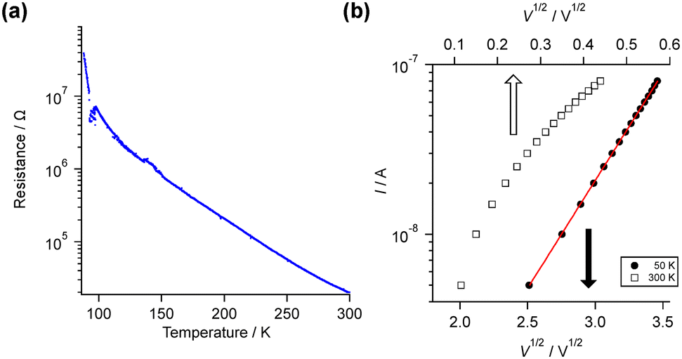
To further elucidate the carrier transport mechanism in C60 nanowires, temperature-dependent conductivity measurements were carried out using FET devices. As shown in Fig. 3(a), the electrical resistivity increases with the decrease in temperature from 300 to 50 K, exhibiting a typical behavior of amorphous organic semiconductors. The same trend was observed upon reheating (Fig. S9, ESI†), confirming the reversibility of the process. This thermally activated behavior suggests that the C60 nanowires fabricated via this method are amorphous. This is consistent with the inherently low crystallinity of pristine C60 condensed phase, as well as the random nature of their polymerization and crosslinking processes. The observed conduction is likely governed by hopping transport of localized charge carriers, rather than band conduction.47 Notably, the I–T characteristics deviate from a linear Arrhenius-type relationship at higher temperatures (∼300 K), implying that temperature-dependent hopping mechanisms need to be considered. To analyze this behavior, the nearest-neighbor hopping (NNH) model48 was applied. As shown in Fig. S10(a) (ESI†), the NNH model fits well in the high-temperature range (250–300 K) but deviates significantly in the low-temperature region (100–250 K). In the NNH framework, charge transport occurs via thermal activation of localized electrons to adjacent vacant sites or deep trap levels near the Fermi level (EF), facilitated by phonon-assisted tunneling. However, at lower temperatures, where phonon contributions become negligible, variable-range hopping (VRH) becomes the dominant transport mechanism. In VRH, carriers hop between more spatially distant localized sites that have minimal energy differences, supported by quantum tunneling.49 To investigate the VRH conduction mechanism, the Mott variable-range hopping model with dimensionality parameter d was employed.50 The model is expressed as follows:
| |  | (3) |
where
G is the electrical conductance,
G0 is a fitting constant,
T is the temperature, and
d represents the dimensionality of the charge transport. By fitting the data with
d = 1, 2, and 3, it was found that the conductance shows a relatively linear dependence with
d = 2 and
d = 3, while a clear deviation from linearity appears with
d = 1, as shown in Fig. S10(b–d) (ESI
†). This indicates that charge transport in these C
60 nanowires occurs in a two- or three-dimensional hopping regime, which implies that the mean free path of the carriers is shorter than the nanowire diameter (∼9.2 nm). Furthermore, in the temperature range below 100 K, the conductance becomes independent of the dimensionality parameter
d, suggesting the dominance of electric-field-driven transport, where carrier injection and tunneling, rather than thermal activation, play the primary roles.
 |
| | Fig. 3 Temperature-dependent electrical conduction measurement of C60 nanowires. (a) Electrical resistance of C60 nanowires plotted against temperature. (b) IDS–VDS curves at different temperatures at 50 and 300 K. These measurements were fixed for W = 200 μm and f = 1 × 1010 cm−2. | |
2.5. Microscopic charge transport in C60 nanowires via time-resolved microwave conductivity
The microscopic electrical conductivity of C60 nanowires was further investigated using non-contact time-resolved microwave conductivity (TRMC) measurements,51–53 as shown in Fig. 4. To enable microwave transmission, horizontally aligned C60 nanowire arrays were fabricated on quartz substrates in the same manner as on silicon substrates. As illustrated in Fig. 4(a), TRMC measurements were performed by orienting the nanowire arrays either parallel or orthogonal to the direction of the microwave electric field oscillation. In the parallel configuration, a clear conductivity signal was observed, whereas in the orthogonal configuration, the signal was negligible. This anisotropic response indicates that carrier mobility is highly directional, aligned along the nanowire axis. These findings further confirm the role of the nanowires as primary pathways for electrical conduction, as shown in Fig. 4(b).
 |
| | Fig. 4 Non-contact electrical conduction measurement of nanowires by TRMC method. (a) Schematic illustration of anisotropic conduction measurement of the nanowire under polarized light. (b) FP-TRMC profiles (λex = 355 nm; photon intensity = 10 mJ cm−2) of C60 nanowire arrays (red: parallel; blue: orthogonal). The inset illustration represents TRMC measurement for horizontally aligned nanowire arrays. Polarized microwaves were injected with electric field oscillation directions parallel or perpendicular along the nanowire arrays. These measurements were fixed for f = 1 × 1011 cm−2. | |
In the TRMC method, the local motion of charge carriers injected into the nanowires is evaluated based on their response to an external alternating-current electric field (E) from a probing microwave at ∼9 GHz. The amplitude of the carrier perturbation (Δx) induced by the oscillating field can be estimated using the linear response theory of diffusive carrier motion, derived from a combination of the Kubo and Einstein–Smoluchowski equations:
| |  | (4) |
where
μ is the carrier mobility,
kB is the Boltzmann constant,
e is the elementary charge, and
ω is the frequency of the microwave.
54 The distinct anisotropic nature of electrical conductivity suggests that the local motion of charge carriers is confined within a 1D cross-section with a diameter of ∼9.2 nm. Given Δ
x ∼ 9.2 nm, the minimum estimate of
μ is 3.5 × 10
−5 m
2 V
−1 s
−1 (0.35 cm
2 V
−1 s
−1) derived from
eqn (4). The recorded maximum value of conductivity in
Fig. 4 is
ϕΣ
μ = ∼0.3 × 10
−9 m
2 V
−1 s
−1 at maximum, leading to the photocarrier generation yield of
ϕ being 10
−4. This is in good agreement with the yield of free carrier generation yield upon excitation to pristine C
60 in the crystalline phase.
55
2.6. Gate voltage dependence and FET characteristics of C60 nanowires
Subsequently, the gate voltage (VGS) was swept across a range of 0, ±10, ±20, ±30, ±40, and ±50 V, and the corresponding drain–source currents were measured (Fig. 5 and Fig. S11, ESI†). As shown in Fig. 5(a), under positive gate voltages, the device exhibited a quasi-linear increase in current, which is characteristic of the linear region of FET operation. In contrast, as seen in Fig. 5(b), little change in current was observed under negative gate voltages. Furthermore, when VDS = +5 V was fixed and the gate voltage was scanned from −50 V to +50 V, the current initially increased and then decreased in the negative gate region (Fig. S12 and S13, ESI†). However, it should be noted that the on/off ratio modulated by the gate voltage was extremely low, as no saturation region was observed in the output characteristics. These behaviors are consistent with those of a depletion-mode n-channel MOSFET,56 suggesting that the majority conduction carriers in the C60 nanowires are electrons. This observation aligns with the well-known properties of C60 as a typical n-type organic semiconductor, widely used in organic thin-film solar cells due to its high electron affinity.57 Moreover, C60 has been reported to exhibit superconductivity and ferromagnetism when combined with alkali metals or other electron-donating species.58–60 The manifestation of n-type FET behavior in the present system implies that the STLiP method preserves the intrinsic electronic characteristics of the C60 molecules, even after polymerization and high-density integration into nanowire arrays. This is a significant observation, as polymerization processes in organic materials often lead to unpredictable changes in electronic structure. Conversely, the absence of a well-defined saturation region in the I–V curves (Fig. S11, ESI†) could be attributed to several factors. These include the presence of contact resistance between the nanowires and electrodes, or damage to the oxide layer on the Si/SiO2 substrate caused by ion beam irradiation. The latter could particularly influence the shape of the I–V characteristics, causing the quasi-linear region to exhibit a continuous increase rather than saturation. Similar behavior has been reported when the electrical connection between the gate and channel is compromised, leading to a linear-like response rather than full FET behavior.61
 |
| | Fig. 5 FET characteristics of C60 nanowires. I–V characteristics (IDSvs. VDS) at (a) VG = 0 to 50 V and (b) VG = 0 to −50 V in a step of 10 V. These measurements were fixed for W = 1500 μm and f = 1 × 1011 cm−2. | |
Finally, the electrical properties of the C60 nanowires were examined after exposure to nitrobenzene vapor.62,63 The nanowire-based FET device was placed in a completely saturated nitrobenzene atmosphere for 10 min. The electrical conductivity was measured immediately after the device was removed into ambient air. As shown in Fig. 6 and Fig. S14, S15 (ESI†), the drain current decreased upon nitrobenzene exposure compared to the measurement in ambient air. Nitrobenzene is a well-known electron-withdrawing molecule, and as the C60 nanowires exhibit n-type conduction with electron carriers, it is presumed that the adsorbed nitrobenzene molecules acted as electron traps, reducing carrier density. Interestingly, as shown in Fig. S16–S18 (ESI†), the conductivity of the nanowires was higher in ambient air than in vacuum, which is contrary to typical behavior observed in conventional semiconductor gas sensors.62,63 In many such systems, oxygen adsorption under atmospheric conditions serves as an electron trap, reducing conductivity. One possible explanation for this discrepancy is that the surface of the C60 nanowires may already be chemically oxidized, thus reducing their sensitivity to additional atmospheric oxygen. Despite this, the detectable change in conductivity upon nitrobenzene exposure suggests that C60 nanowires may still serve as viable sensing elements in semiconductor-based gas sensors. The saturated vapor concentration of nitrobenzene is approximately 322 ppm,64 which falls within the typical detection range of commercial gas sensors.
 |
| | Fig. 6 Electrical conduction property changes due to gas molecule adsorption. I–V characteristics (IDSvs. VDS), at VG = 0, before (dotted line) and after (solid line) adsorption of nitrobenzene. These measurements were fixed for W = 1500 μm and f = 1 × 1011 cm−2. | |
3. Conclusions
In this study, we sought to elucidate the conduction mechanism in one-dimensional organic nanomaterials based on C60 nanowires after evaluating their electrical properties. An ion beam with a freely adjustable irradiation angle was used to fabricate nanowire arrays oriented vertically and horizontally onto the support substrate, respectively, and the devices were prepared for electrical characterization. Grazing incidence of a high-energy ion beam allows us to efficiently utilize the energy released from the particle to fabricate uniform C60 nanowires with >10 μm total length, which demonstrates over one order of magnitude higher efficiency of nanowire production in comparison with orthogonal incidence of ion beams, giving vertically aligned nanowire arrays. The C60 nanowires showed very large electrical conductivity, which was suggested to be due to the special polymerization process of the C60 monomer. From the nanowire FET devices, it was concluded that the conduction carrier of C60 nanowires is an electron, and the temperature-dependent conduction properties suggest that it is based on a hopping conduction mechanism. As an application, we explored the use of C60 nanowires in current-sensing gas sensors.
4. Experimental
4.1. Materials
C60, rubrene, and TiOPc were purchased from Tokyo Chemical Industry (Japan) and used without further purification. o-Dichlorobenzene was purchased from FUJIFILM Wako Pure Chemical Corporation (Japan) and used without further purification.
4.2. Film preparation
Doped-Si (n-type) and quartz glass substrates were cut into 1 cm2 squares, sonicated in acetone and then 2-propanol, dried, and treated via plasma cleaning prior to use. All thin films were prepared via vapor deposition under ∼10−4 Pa at a rate of 0.2–0.6 Å s−1. The thicknesses of the films were evaluated using a Dektak XT-E (Bruker, Billerica, MA, USA).
4.3. Irradiation and isolation
129Xe23+ (450 MeV) was generated using an AVF cyclotron accelerator at Takasaki Institute for Advanced Quantum Science, National Institutes for Quantum Science and Technology, Takasaki, Japan. The prepared organic films were exposed to the ion beam in a vacuum chamber (<1 × 10⁻⁴ Pa). The number of incident particles was controlled at a fluence of 109–1011 cm−2 by setting the exposure time (s) and flux (cm−2 s−1) calculated using the beam current, charges of the ions used, and elementary charge. The irradiated films were developed by immersing them in organic solvents and dried in air.
4.4. Monte Carlo method simulation of ion beams
The simulation was performed using SRIM-2013,65 assuming 10![[thin space (1/6-em)]](https://www.rsc.org/images/entities/char_2009.gif) 000 Xe ions (450 MeV) incident normally on a condensed-phase C60 target with a density of 1.72 g cm−3. Although the actual experiment used grazing incidence to form horizontally aligned nanowires, orthogonal incidence was adopted in the simulation for simplicity. In this simulation, the C60 target was assumed to be structurally equivalent in both its thin-film and crystalline phases, based on the premise that energy dissipation behavior under energetic ion irradiation is comparable in both phases. As the LET primarily depends on the ion energy and the target density, this simplification does not significantly affect the interpretation of energy transfer characteristics.
000 Xe ions (450 MeV) incident normally on a condensed-phase C60 target with a density of 1.72 g cm−3. Although the actual experiment used grazing incidence to form horizontally aligned nanowires, orthogonal incidence was adopted in the simulation for simplicity. In this simulation, the C60 target was assumed to be structurally equivalent in both its thin-film and crystalline phases, based on the premise that energy dissipation behavior under energetic ion irradiation is comparable in both phases. As the LET primarily depends on the ion energy and the target density, this simplification does not significantly affect the interpretation of energy transfer characteristics.
4.5. Morphological characterization of the nanowires
The sizes and shapes of the isolated nanowires were observed using a MultiMode 8 AFM (Bruker, US), JSM-7001F SEM system (JEOL, Japan), and JEM-2100F(G5) TEM system (JEOL, Japan).
4.6. Photolithography
After spin coating the photoresist AZ1500 on the nanowire substrate after isolation, UV exposure was performed on each electrode pattern. After appropriate processing with a developing solution, Ti: 2 nm and Au: 50 nm were deposited by the sputtering method. The source–drain electrodes were then created by lifting them off with acetone heated to 100 °C.
4.7. Electrical conductivity measurement
Electrical conductivity measurements were carried out under atmospheric pressure and in a vacuum (<10−2 Pa) by a TTPX cryogenic probe station (Lake Shore, Westerville, US), and those at low temperatures (50–300 K) were carried out in a low vacuum (∼100 Pa) by CFMS-base-9T (Cryogenic, London, UK).
4.8. TRMC measurement
TRMC measurements were carried out with probing microwave at 9 GHz, 3 mW. The set of apparatus was described elsewhere.66
Author contributions
M. N., S. S., M. K., A. T., H. I., A. I., and T. Y. irradiated samples with ion beams. M. N., S. S., M. K., A. T., and H. I. fabricated organic nanowires. M. N. S. S., M. K., and K. K. fabricated C60 nanowire devices. M. N., S. S., M. K., K. K., Y. T., and M. S. evaluated their electrical properties. M. N. wrote the manuscript. S. S. supervised the work and revised the manuscript. All authors contributed to the discussion of the results and the preparation of the manuscript.
Data availability
The data that support the findings of this study are available in the main text and ESI.†
Conflicts of interest
There are no conflicts to declare.
Acknowledgements
The Japan Society for the Promotion of Science (JSPS) and Japan Science and Technology Agency (JST) provided funding for this work through a Research Fellow of the JSPS, a Grant-in-Aid for the Transformative Research Area “Condensed Conjugation”, and Grants-in-Aid for a JSPS Research Fellow (grant number: 23KJ1261), Scientific Research (grant numbers: 23H05462, 22H00314, 20H05867, and 20H05862), and JST-CREST (grant number: JPMJCR23O3). This work was supported by the commissioned research fund from F-REI (JPFR24080202).
References
- N. Baig, I. Kammakakam and W. Falath, Mater. Adv., 2021, 2, 1821–1871 RSC.
- L. A. Kolahalam, I. V. Kasi Viswanath, B. S. Diwakar, B. Govindh, V. Reddy and Y. L. N. Murthy, Mater. Today: Proc., 2019, 18, 2182–2190 Search PubMed.
- C. Tan, X. Cao, X.-J. Wu, Q. He, J. Yang, X. Zhang, J. Chen, W. Zhao, S. Han, G.-H. Nam, M. Sindoro and H. Zhang, Chem. Rev., 2017, 117, 6225–6331 CrossRef CAS.
- D. Jariwala, V. K. Sangwan, L. J. Lauhon, T. J. Marks and M. C. Hersam, Chem. Soc. Rev., 2013, 42, 2824–2860 RSC.
- Y.-F. Wang, L. Zhu, L. Han, X.-H. Zhou, Y. Gao and L.-H. Lv, ACS Appl. Nano Mater., 2023, 6, 7107–7122 CrossRef CAS.
- C. Jia, Z. Lin, Y. Huang and X. Duan, Chem. Rev., 2019, 119, 9074–9135 CrossRef CAS.
- L. N. Quan, J. Kang, C.-Z. Ning and P. Yang, Chem. Rev., 2019, 119, 9153–9169 CrossRef CAS.
- N. P. Dasgupta, J. Sun, C. Liu, S. Brittman, S. C. Andrews, J. Lim, H. Gao, R. Yan and P. Yang, Adv. Mater., 2014, 26, 2137–2184 CrossRef CAS PubMed.
- Y. Xia, P. Yang, Y. Sun, Y. Wu, B. Mayers, B. Gates, Y. Yin, F. Kim and H. Yan, Adv. Mater., 2003, 15, 353–389 CrossRef CAS.
- J. S. Meyer and K. A. Matveev, J. Phys.: Condens. Matter, 2009, 21, 023203 CrossRef PubMed.
- C. H. L. Quay, T. L. Hughes, J. A. Sulpizio, L. N. Pfeiffer, K. W. Baldwin, K. W. West, D. Goldhaber-Gordon and R. de Picciotto, Nat. Phys., 2010, 6, 336–339 Search PubMed.
- O. Hayden, R. Agarwal and W. Lu, Nano Today, 2008, 3, 12–22 CrossRef CAS.
- L. Mai, X. Tian, X. Xu, L. Chang and L. Xu, Chem. Rev., 2014, 114, 11828–11862 CrossRef CAS PubMed.
- N. S. Ramgir, Y. Yang and M. Zacharias, Small, 2010, 6, 1705–1722 CrossRef CAS.
- S. W. Eaton, A. Fu, A. B. Wong, C.-Z. Ning and P. Yang, Nat. Rev. Mater., 2016, 1, 16028 CrossRef CAS.
- A. I. Hochbaum and P. Yang, Chem. Rev., 2010, 110, 527–546 CrossRef CAS.
- A. I. Boukai, Y. Bunimovich, J. Tahir-Kheli, J.-K. Yu, W. A. Goddard Iii and J. R. Heath, Nature, 2008, 451, 168–171 CrossRef CAS PubMed.
- Y.-L. Shi and X.-D. Wang, Adv. Funct. Mater., 2021, 31, 2008149 CrossRef CAS.
- S.-Y. Min, T.-S. Kim, Y. Lee, H. Cho, W. Xu and T.-W. Lee, Small, 2015, 11, 45–62 CrossRef CAS.
- A. L. Briseno, S. C. B. Mannsfeld, S. A. Jenekhe, Z. Bao and Y. Xia, Mater. Today, 2008, 11, 38–47 CrossRef CAS.
- S. Gong and W. Cheng, Adv. Electron. Mater., 2017, 3, 1600314 CrossRef.
- J.-L. Wang, M. Hassan, J.-W. Liu and S.-H. Yu, Adv. Mater., 2018, 30, 1803430 CrossRef.
- C. Zhang, C.-L. Zou, H. Dong, Y. Yan, J. Yao and Y. S. Zhao, Sci. Adv., 2017, 3, e1700225 CrossRef PubMed.
- L. Zang, Y. Che and J. S. Moore, Acc. Chem. Res., 2008, 41, 1596–1608 CrossRef CAS PubMed.
- A. Borras, O. Gröning, M. Aguirre, F. Gramm and P. Gröning, Langmuir, 2010, 26, 5763–5771 CrossRef CAS.
- S. Chakraborty, S. Varghese and S. Ghosh, Chem. – Eur. J., 2019, 25, 16725–16731 CrossRef CAS PubMed.
- K. M. Alam, A. P. Singh, R. Starko-Bowes, S. C. Bodepudi and S. Pramanik, Adv. Funct. Mater., 2012, 22, 3298–3306 CrossRef CAS.
- W. Deng, X. Zhang, L. Wang, J. Wang, Q. Shang, X. Zhang, L. Huang and J. Jie, Adv. Mater., 2015, 27, 7305–7312 CrossRef CAS.
- J. Samà, G. Domènech-Gil, I. Gràcia, X. Borrisé, C. Cané, S. Barth, F. Steib, A. Waag, J. D. Prades and A. Romano-Rodríguez, Sens. Actuators, B, 2019, 286, 616–623 CrossRef.
- J. E. E. Baglin, Appl. Surf. Sci., 2012, 258, 4103–4111 CrossRef CAS.
- H. Cho, S.-Y. Min and T.-W. Lee, Macromol. Mater. Eng., 2013, 298, 475–486 CrossRef CAS.
- S. Sakaguchi, K. Kamiya, T. Sakurai and S. Seki, Quant. Beam Sci., 2020, 4, 7–28 CrossRef CAS.
- S. Sakaguchi, T. Sakurai, J. Ma, M. Sugimoto, T. Yamaki, A. Chiba, Y. Saito and S. Seki, J. Phys. Chem. B, 2018, 122, 8614–8623 CrossRef CAS.
- T. Sakurai, S. Sakaguchi, Y. Takeshita, K. Kayama, A. Horio, M. Sugimoto, T. Yamaki, A. Chiba, Y. Saitoh, L. B. V. S. Garimella, D. K. Avasthi and S. Seki, ACS Appl. Nano Mater., 2020, 3, 6043–6053 CrossRef CAS.
- K. Kamiya, K. Kayama, M. Nobuoka, S. Sakaguchi, T. Sakurai, M. Kawata, Y. Tsutsui, M. Suda, A. Idesaki, H. Koshikawa, M. Sugimoto, G. B. V. S. Lakshmi, D. K. Avasthi and S. Seki, Nat. Commun., 2021, 12, 4025 CrossRef CAS.
- Y. Maeyoshi, A. Saeki, S. Suwa, M. Omichi, H. Marui, A. Asano, S. Tsukuda, M. Sugimoto, A. Kishimura, K. Kataoka and S. Seki, Sci. Rep., 2012, 2, 600 CrossRef PubMed.
- D. J. Thomas, Radiat. Prot. Dosim., 2012, 150, 550–552 CrossRef.
- M. Omichi, H. Marui, V. S. Padalkar, A. Horio, S. Tsukuda, M. Sugimoto and S. Seki, Langmuir, 2015, 31, 11692–11700 CrossRef CAS.
- S. Tsukuda, S. Seki, M. Sugimoto and S. Tagawa, J. Phys. Chem.
B, 2006, 110, 19319–19322 CrossRef CAS.
- M. Nobuoka, K. Kamiya, S. Sakaguchi, A. Idesaki, T. Yamaki, T. Sakurai and S. Seki, J. Photopolym. Sci. Technol., 2021, 34, 167–174 CrossRef CAS.
- P. Hu, X. He and H. Jiang, InfoMat, 2021, 3, 613–630 CrossRef CAS.
- S. M. Sze and J. C. Irvin, Solid-State Electron., 1968, 11, 599–602 CrossRef CAS.
- C. Wen, J. Li, K. Kitazawa, T. Aida, I. Honma, H. Komiyama and K. Yamada, Appl. Phys. Lett., 1992, 61, 2162–2163 CrossRef CAS.
- J. Onoe, T. Nakayama, M. Aono and T. Hara, J. Phys. Chem. Solids, 2004, 65, 343–348 CrossRef CAS.
- A. M. Rao, P. C. Eklund, U. D. Venkateswaran, J. Tucker, M. A. Duncan, G. M. Bendele, P. W. Stephens, J.-L. Hodeau, L. Marques, M. Núñez-Regueiro, I. O. Bashkin, E. G. Ponyatovsky and A. P. Morovsky, Appl. Phys. A, 1997, 64, 231 CrossRef CAS.
- Y. Lwasa, T. Arima, R. M. Fleming, T. Siegrist, O. Zhou, R. C. Haddon, L. J. Rothberg, K. B. Lyons, H. L. CarterJr, A. F. Hebard, R. Tycko, G. Dabbagh, J. J. Krajewski, G. A. Thomas and T. Yagi, Science, 1994, 264, 1570 CrossRef.
- V. Coropceanu, J. Cornil, D. A. da Silva Filho, Y. Olivier, R. Silbey and J.-L. Brédas, Chem. Rev., 2007, 107, 926–952 CrossRef CAS PubMed.
- R. P. Fornari and A. Troisi, Phys. Chem. Chem. Phys., 2014, 16, 9997–10007 RSC.
- R. M. Hill, Phys. Status Solidi A, 1976, 34, 601–613 CrossRef CAS.
- N. F. Mott, J. Non-Cryst. Solids, 1968, 1, 1–17 CrossRef CAS.
- S. Seki, R. P. Paitandi, W. Choi, S. Ghosh and T. Tanaka, Acc. Chem. Res., 2024, 57, 2665–2677 CrossRef CAS PubMed.
- S. Seki, A. Saeki, T. Sakurai and D. Sakamaki, Phys. Chem. Chem. Phys., 2014, 16, 11093–11113 RSC.
- T. Amaya, S. Seki, T. Moriuchi, K. Nakamoto, T. Nakata, H. Sakane, A. Saeki, S. Tagawa and T. Hirao, J. Am. Chem. Soc., 2009, 131, 408–409 CrossRef CAS.
- R. Kubo, Rep. Prog. Phys., 1966, 29, 255–284 CrossRef CAS.
- J. H. Choi, T. Honda, S. Seki and S. Fukuzumi, Chem. Commun., 2011, 47, 11213–11215 RSC.
- J. Rivnay, S. Inal, A. Salleo, R. M. Owens, M. Berggren and G. G. Malliaras, Nat. Rev. Mater., 2018, 3, 17086 CrossRef CAS.
- R. Ganesamoorthy, G. Sathiyan and P. Sakthivel, Sol. Energy Mater. Sol. Cells, 2017, 161, 102–148 CrossRef CAS.
- A. F. Hebard, M. J. Rosseinsky, R. C. Haddon, D. W. Murphy, S. H. Glarum, T. T. M. Palstra, A. P. Ramirez and A. R. Kortan, Nature, 1991, 350, 600–601 CrossRef CAS.
- Y. Zhao, Y. Guo, Y. Qi, X. Jiang, Y. Su and J. Zhao, Adv. Sci., 2023, 10, 2301265 CrossRef CAS.
- S.-Z. Wang, M.-Q. Ren, S. Han, F.-J. Cheng, X.-C. Ma and C.-L. Song, Commun. Phys., 2021, 4, 114 CrossRef CAS.
- K. Ogawa, T. Kato, A. Ikegami, H. Tsuji, N. Aoki, Y. Ochiai and J. P. Bird, Appl. Phys. Lett., 2006, 88, 112109 CrossRef.
- P. Raju and Q. Li, J. Electrochem. Soc., 2022, 169, 057518 CrossRef CAS.
- B. Yang, N. V. Myung and T.-T. Tran, Adv. Electron. Mater., 2021, 7, 2100271 CrossRef CAS.
-
T. E. Daubert and R. P. Danner, Physical and thermodynamic properties of pure chemicals: data compilation, Taylor & Francis,Washington, DC, 1989 Search PubMed.
- J. F. Ziegler, M. D. Ziegler and J. P. Biersack, Nucl. Instrum. Methods Phys. Res., Sect. B, 2010, 268, 1818–1823 CrossRef CAS.
- S. Seki, R. P. Paitandi, W. Choi and T. Tanaka, Acc. Chem. Res., 2024, 57, 2665 CrossRef CAS PubMed.
|
| This journal is © The Royal Society of Chemistry 2025 |
Click here to see how this site uses Cookies. View our privacy policy here. 
 Open Access Article
 This Open Access Article is licensed under a Creative Commons Attribution-Non Commercial 3.0 Unported Licence
 ac,
Masayuki
Suda
ad,
Haruka
Inoue
a,
Akira
Idesaki
b,
Tetsuya
Yamaki
b and
Shu
Seki
ac,
Masayuki
Suda
ad,
Haruka
Inoue
a,
Akira
Idesaki
b,
Tetsuya
Yamaki
b and
Shu
Seki