
Modulating hot carrier relaxation and trapping dynamics in lead halide perovskite nanoplatelets by surface passivation†
Yanshen
Zhu
,
Shida
Luo
,
Yuting
Zhang
,
Yanping
Liu
,
Yulu
He
,
Tianfeng
Li
,
Zhen
Chi
* and
Lijun
Guo
 *
*
School of Physics and Electronics, International Joint Research Laboratory of New Energy Materials and Devices of Henan Province, Henan University, Kaifeng 475004, China. E-mail: zhenchi@henu.edu.cn; juneguo@henu.edu.cn
First published on 22nd November 2024
Abstract
Two-dimensional (2D) lead halide perovskite (LHP) nanoplatelets (NPLs) have recently emerged as promising materials for solar cells and light-emitting devices. The reduction of LHP dimensions introduces an abundance of surface defects, which can strongly influence the photophysical properties of these materials. However, an insightful understanding of the effect of surface defects on hot carrier (HC) relaxation, one of the important properties of LHP NPLs, is still inadequate. Herein, the HC relaxation and trapping dynamics in pristine and surface passivated two-layer (2L) CsPbBr3 NPLs have been investigated by using time-resolved spectroscopy. The results reveal that surface defects can trap HCs directly before they relax to the band edge, which accounts for the absence of the hot-phonon bottleneck (HPB) effect in LHP NPLs. After healing surface defects with a passivation agent, the relaxation time of HCs is extended from ∼73 to ∼130 fs in 2L CsPbBr3 NPLs, indicating that the channel of HCs trapped by the surface defects can be effectively blocked. Accordingly, the HPB effect is activated in surface-passivated CsPbBr3 NPLs. The finding of surface defect-related HC relaxation dynamics is important for guiding the development of high-performance LHP NPL devices related to HCs through surface defect engineering.
Introduction
Two-dimensional (2D) lead halide perovskite (LHP) nanoplatelets (NPLs) have emerged as a new class of semiconductor materials for solar cells and light-emitting devices.1–5 Compared to their bulk counterparts, atomically thin LHP NPLs exhibit many interesting characteristics, such as high exciton binding energy, large absorption cross sections, narrow emission peaks, adjustable band gap through thickness and composition control, easy surface modification,6–10 and so on. However, as the dimensionality of LHPs decreases, the surface-to-volume ratio increases, inevitably producing an abundance of surface defects, which can strongly influence the photophysical properties of these atomically thin materials.11,12 Although many studies on defect-related carrier dynamics in 2D LHP NPLs have been reported, most of them have focused on uncovering the impact of defects on the band edge carrier dynamics,13–16 and understanding of how the hot carriers (HCs) interact with the surface defects in 2D LHP NPLs is still inadequate.When a semiconductor is excited using photons with energies greater than its band gap, the photogenerated carriers in the semiconductor have significantly higher energies than the band edge before they dissipate the energy to the lattice and are often referred to as HCs. HCs carry a large amount of energy, which can drive chemical and physical processes.17–19 For optoelectronic devices, longer-lived HCs are needed to further increase the power conversion efficiency to overcome the Shockley–Queisser limit.20 In 0D and 3D-like LHPs,21–23 the relaxation time of HCs can be significantly prolonged via the hot-phonon bottleneck (HPB) effect under high excitation fluences. However, many studies have reported that no HPB effect was observed in the HC relaxation of 2D LHP NPLs, and different views have been proposed for the HPB-free HC relaxation.24–28 For example, Feldmann et al. and Ghosh et al. suggested that the lack of the HPB effect in 2D LHP NPLs is due to the reduced screening of the Coulomb-mediated carrier-phonon interaction in their low-dielectric surroundings.24,25 Recently, Sun et al. attributed the absence of the HPB effect in 2D LHP NPLs to the efficient out-of-plane triplet-exciton-LO–phonon coupling because of the structural anisotropy.27 In 2023, Bakulin's group observed that the highly excited HCs in monolayer WS2 can be trapped during relaxation by defects.29 Inspired by this work, the increased surface defects because of the increased ratio of surface-to-volume in 2D LHP NPLs may also account for the different HC relaxation dynamics compared with that in 0D and 3D-like LHPs. Therefore, it is necessary to gain a deeper understanding of the influence of surface defects on the HC relaxation process in 2D LHP NPLs.
To investigate the effect of surface defects on the HC relaxation process, in this work, pristine and surface passivated two-layer (2L) CsPbBr3 NPLs were synthesized, and their ultrafast HC dynamics were comprehensively investigated by using both transient absorption (TA) and time-resolved photoluminescence (PL) spectroscopy. The direct trapping of HCs by surface defects during relaxation was observed. The process of HC relaxation was found to slow down in passivated 2L CsPbBr3 NPLs, which arises from the reduced surface defects by the addition of a passivation agent. The regulation of HC relaxation time by surface defect engineering in 2L LHP NPLs can facilitate their application in photovoltaic and optoelectronic devices related to HCs.
Results and discussion
In the present study, our main aim is to examine the effect of surface defects on the process of HC relaxation in 2D LHP NPLs. Considering that the surface defect density and volume ratio of NPLs increase with the decrease of NPL thickness, 2L ultrathin CsPbBr3 perovskite NPLs were selectively prepared following a reported method with slight modifications (see the Experimental section in the ESI† for details).30,31 As presented in Fig. 1a, to heal the surface defects of the as-prepared CsPbBr3 NPLs, a hexane solution of PbBr2, oleic acid, and oleylamine was used according to a previously reported literature method.32 Herein, the as-synthesized and surface-passivated NPLs are named A-NPLs and P-NPLs for easy distinction. Fig. 1b–e show transmission electron microscope (TEM) images of the synthesized CsPbBr3 NPLs. The TEM images reveal that the morphology of the NPLs is maintained after the surface passivation process in our experiments. Both the A-NPLs and P-NPLs prepared in our experiments display a rectangular shape with an average length of ∼12 nm and width of ∼7 nm (Fig. 1b, d, and S1†), respectively. The average thickness of the A-NPLs and P-NPLs with a value of ∼1.5 nm is confirmed by the TEM images of NPLs standing on their side (Fig. 1c, e, and S1†). Therefore, the measured thickness (∼1.5 nm) in our experiments corresponds to the NPL comprising two monolayers, according to the ∼0.6 nm lattice parameter of the CsPbBr3 cubic crystal structure.31,33 The as-prepared NPLs adopt a cubic perovskite phase, which will be demonstrated below via X-ray diffraction (XRD) analysis.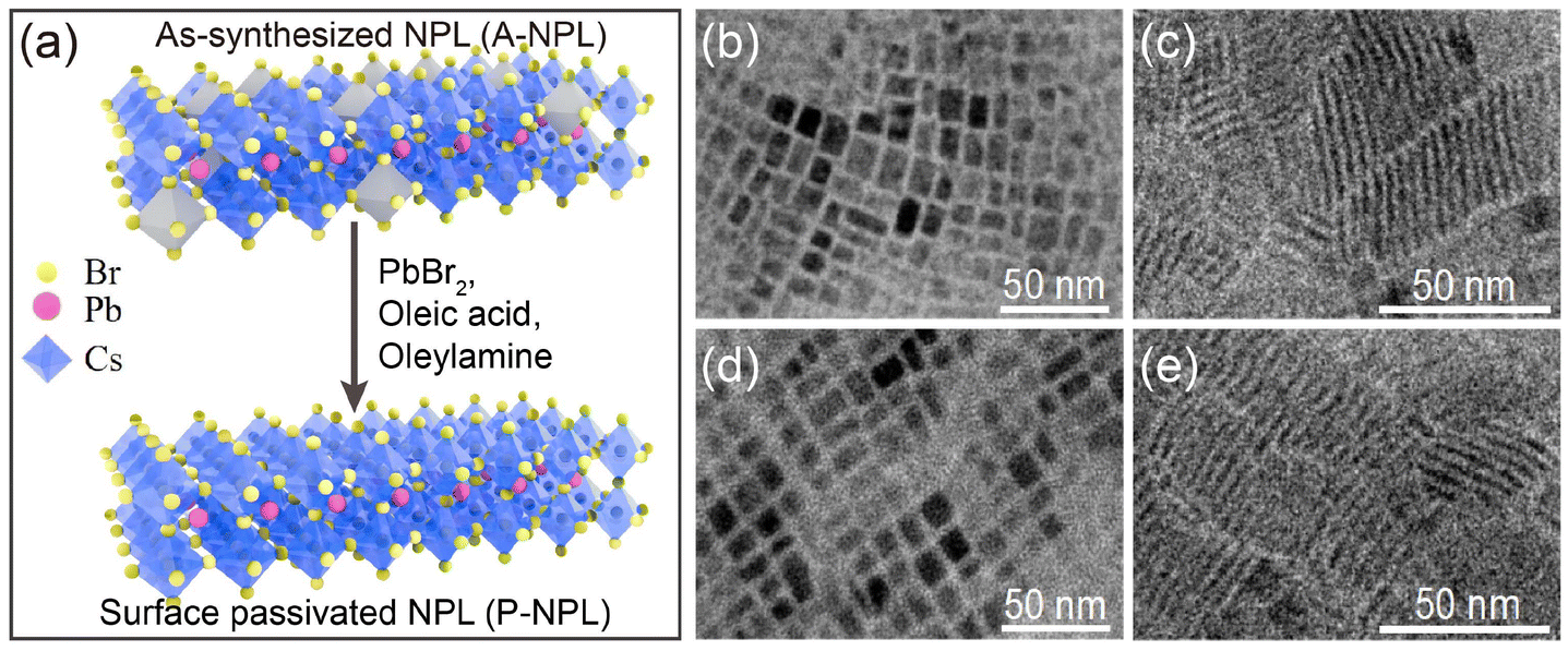 | ||
| Fig. 1 (a) Schematic of the passivation method that converts A-NPL into P-NPL. The gray octahedron in the lattice of A-NPL denotes the Pb2+ vacancy. TEM images of tiled (b) and vertical (c) A-NPLs. TEM images of tiled (d) and vertical (e) P-NPLs. | ||
Fig. 2a shows the XRD patterns of the prepared A-NPLs and P-NPLs in our experiments, with the standard pattern of the CsPbBr3 cubic phase (PDF# 54-0752) added for comparison.34 From the XRD data, we clearly identified that the phase of CsPbBr3 NPLs is retained after passivation and they have a cubic phase consistent with the standard pattern. Three intense diffraction peaks appearing at ∼15.6, ∼21.9, and ∼30.9° in the XRD patterns are assigned to the (100), (110), and (200) crystallographic facets, respectively.35 It is well known that the contribution to the electronic structure near the band edges of CsPbBr3 primarily arises from Br 4p and Pb 6p orbitals, while the Cs ion plays a minor role.36,37 This is because cubic CsPbBr3 consists of periodically arranged Pb–Br octahedra that show strong interactions, while the isolated Cs ions at the corners of the cube exhibit weak interactions. Therefore, the optical properties of CsPbBr3 NPLs can be easily modulated through variation of the surface Pb and Br states since internal defects are negligible compared to surface defects due to their massive exposed surfaces. In general, two types of lead and bromine vacancy defects (VPb and VBr) exist on the surface of CsPbBr3 NPLs. To confirm the difference in the surface chemical states of A-NPLs and P-NPLs, X-ray photoelectron spectroscopy (XPS) measurements were performed on the two samples. Fig. 2b–d show the XPS spectra of Cs 3d, Pb 4f, and Br 3d for pristine A-NPLs and surface passivated P-NPLs. The Cs 3d XPS spectra display no change after passivation treatment, confirming the weak interaction between Cs+ and the PbBr64− octahedron as discussed above. In the Pb 4f XPS spectra, two main peaks appear in the curves of both samples and two minor peaks can be seen at low binding energy sites after fitting. The main and minor peaks are assigned to the inner and surface Pb ions,38–40 respectively. After passivation, the intensity ratio between inner and surface ions increases and the peaks shift to a higher binding energy side, indicating that the level of Pb–Br species increases at the surface. In other words, the VBr defect density on the CsPbBr3 surface of NPLs decreases after passivation due to Pb ions only bonding with Br ions in the crystal lattice. In addition, as shown in Fig. 2d, the increase in the level of Pb–Br species in P-NPLs can also be confirmed by the shift of the peaks in the Br 3d spectra. By calculating the peak areas in XPS data and atomic sensitivity factors, the relative ratios of Cs, Pb, and Br in A-NPLs and P-NPLs are found to be 1![[thin space (1/6-em)]](https://www.rsc.org/images/entities/char_2009.gif) :1:2.8 and 1:1.1:3.5, respectively. Therefore, the XPS data above prove that the surface defects of VBr and VPb are lower for the P-NPLs than the A-NPLs.
:1:2.8 and 1:1.1:3.5, respectively. Therefore, the XPS data above prove that the surface defects of VBr and VPb are lower for the P-NPLs than the A-NPLs.
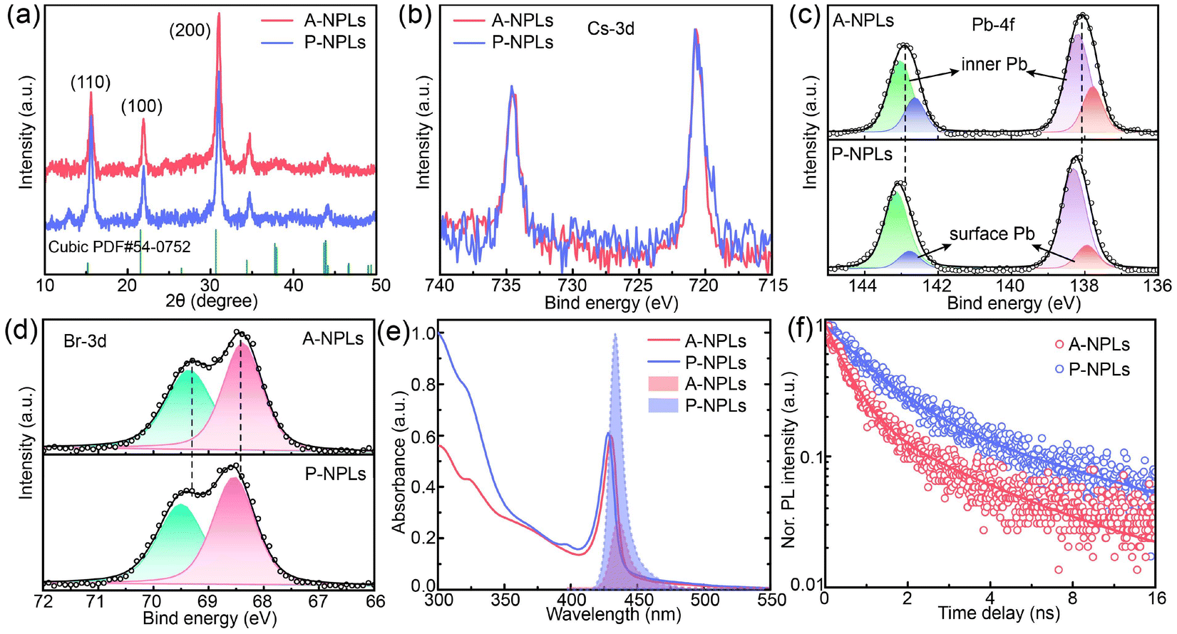 | ||
| Fig. 2 (a) XRD patterns of pristine and surface passivated 2L CsPbBr3 NPLs. (b) XPS spectra of Cs 3d (b), Pb 4f (c), and Br 3d (d) of pristine and surface passivated 2L CsPbBr3 NPLs. (e) Steady-state absorption and PL spectra of pristine and surface passivated 2L CsPbBr3 NPLs in hexane solution. (f) Normalized PL decay dynamics of pristine and surface passivated 2L CsPbBr3 NPLs. The open circles and curves in (f) are the experimental data and biexponential fitting results, respectively. | ||
To explore the optical properties of the A-NPLs and P-NPLs, steady-state UV-vis absorption and PL spectra were first recorded. As shown in Fig. 2e, the absorption spectrum of A-NPLs shows a sharp exciton absorption peak at ∼430 nm with a half-maximum full width of ∼11 nm. The narrow and single absorption peak suggests that the NPLs have a good size distribution and shape uniformity. The PL peak of A-NPLs appears at ∼436 nm in the emission spectrum (Fig. 2e, pink shadow). After passivation, the spectral shapes of the excitonic absorption and PL emission remain almost unchanged, implying that the thickness of the NPLs does not change, which is consistent with the results of TEM. Both the excitonic absorption and PL emission peaks of NPLs display a slight blue shift after passivation, which can be attributed to the enhancement of the dielectric effect. Specifically, the intensity of the PL emission of P-NPLs is significantly enhanced compared with that of the A-NPLs (Fig. 2e), with the PL quantum yield (QY) increasing from 15.2% to 48.7% (see Note 1 in the ESI† for the method). This increase of PL QY in passivated NPLs indicates the suppression of defect-related non-radiative carrier recombination after introducing the passivation agent. Next, time-resolved PL (TRPL) measurements were conducted on A-NPLs and P-NPLs under excitation at 375 nm to study the effect of passivation on the exciton recombination process of NPLs. As illustrated in Fig. 2f, both the PL decay curves of A-NPLs and P-NPLs detected at 435 nm can be well fitted with a biexponential function (see Note 2 in the ESI†), and the corresponding decay parameters are listed in Table S1.† However, compared with the pristine A-NPLs, the average PL lifetime of P-NPLs is prolonged from 3.68 ± 0.57 ns to 7.24 ± 0.90 ns due to the highly suppressed non-radiative carrier recombination channel in P-NPLs (Table S1†), further confirming the decrease in surface defect density after passivation in NPLs.41,42
In order to investigate the HC relaxation dynamics in CsPbBr3 NPLs, we carried out systematic TA measurements on the pristine and surface passivated samples under the above band gap excitation (360 nm). Fig. 3a–d display the typical TA mapping and spectra at selected time delays of A-NPLs and P-NPLs. The TA spectra of both samples are dominated by a strong and narrow photobleaching (PB) feature centered at ∼430 nm, matching the peak of the excitonic transition in the steady-state UV-vis absorption spectra (Fig. 2e), which can be attributed to the state-filling effects.43 In addition, the TA spectra also present two photoinduced absorption peaks located beside the PB signal, which may be caused by the absorption of the photoinduced carriers, band gap renormalization, and biexciton effect.25,44,45 However, the exciton PB signals of pristine CsPbBr3 NPLs show a faster recovery than that of surface passivated CsPbBr3 NPLs, which is consistent with the result obtained in TRPL measurements (Fig. 2f) and further suggests the reduction of surface defects in passivated CsPbBr3 NPLs. We have further monitored and compared the exciton PB dynamics of pristine and surface passivated CsPbBr3 NPLs extracted from Fig. 3a and b. As shown in Fig. 3e, the exciton PB dynamics detected at ∼430 nm confirms the slow recovery in passivated CsPbBr3 NPLs. The PB recovery dynamics can be fitted with a multi-exponential decay function (solid curves in Fig. 3e). The decay time constants are 0.32 ± 0.05 ps (61%), 130 ± 13 ps (24%), and 4170 ± 400 ps (15%) for pristine CsPbBr3, and 0.36 ± 0.07 ps (60%), 210 ± 15 ps (24%), and 9205 ± 900 ps (16%) for passivated CsPbBr3 NPLs. The two fast decay components can be assigned to the trapping of carriers by shallow and deep defect states,16 and the slow component could be attributed to carrier radiative recombination.46 Meanwhile, as illustrated in Fig. 3f, the buildup of PB dynamics with a sub-picosecond time constant was observed, which reflects the process of HC generation by photon excitation with energy larger than the band gap relaxing from a high energy level to form the subsequent exciton.47 The HC relaxation time of CsPbBr3 NPLs can be extracted by exponential fitting and increases from ∼73 fs to ∼130 fs after surface passivation. We speculate that the slow relaxation rate of HCs in P-NPLs observed under the same experimental conditions can be attributed to the suppression of HCs trapped by surface defects. The surface defect density controls and determines the competition between HC relaxation and carrier trapping in NPLs. Since the probability of HCs being trapped by surface defects in A-NPLs is higher, the observed HC lifetime is shorter, which is reflected in the rapid rise of the exciton PB dynamics. Similarly, the trapping of highly excited HCs in monolayer WS2 during cooling by defects has been demonstrated in recently reported work.29
 | ||
| Fig. 3 TA mapping as a function of probe wavelength and time delay under 360 nm excitation with a pump power of 0.3 μW for pristine (a) and surface passivated (b) 2L CsPbBr3 NPLs. (c) and (d) TA spectra probed at the selected delay times extracted from (a) and (b), respectively. (e) Normalized exciton dynamics of pristine and surface passivated 2L CsPbBr3 NPLs. (f) The zoomed-in profiles of (e) in the earlier time delay. The open circles in (e) and (f) represent the experimental data, and the curves show the multi-exponential fitting results after the consideration of the instrument response function (IRF, ∼120 fs). | ||
To verify the speculation proposed above and deeply understand the impact of surface defects on HC relaxation in CsPbBr3 NPLs, TA measurements on pristine and surface passivated CsPbBr3 NPLs under near band edge excitation (405 nm) were further performed in our experiments. As shown in Fig. S2 and S3,† similar to that of 360 nm excitation, the exciton PB dynamics of CsPbBr3 NPLs recover with a much slower rate after surface passivation due to the suppression of defect-related non-radiative carrier recombination. However, compared with the 360 nm excitation, the difference is that the exciton PB dynamics of pristine and surface passivated CsPbBr3 NPLs show a more rapid rising process and reach their maximum simultaneously, as illustrated in Fig. 4a. The rapid rise of the PB dynamics under 405 nm excitation is because the carriers generated in CsPbBr3 NPLs excited with the wavelength close to the exciton absorption are mainly near the band edge, which can be detected immediately by the probe pulse after photoexcitation, resulting in a fast PB dynamics buildup rate. This result further confirms that the accelerated HC relaxation in pristine CsPbBr3 NPLs under 360 nm excitation (Fig. 3f) results from the direct trapping of HCs by surface defects. Next, the pump intensity-dependent HC relaxation dynamics were measured under 360 nm excitation to examine whether the HPB effect was present in CsPbBr3 NPLs. As displayed in Fig. 4b, the buildup of PB dynamics in pristine CsPbBr3 NPLs exhibits no dependence on the pump intensity, implying a lack of the HPB effect in this material, which is in accord with earlier reports.26,27 As discussed above, the high density of surface defects in the pristine CsPbBr3 NPLs can trap the HCs directly, and then the excess energy carried by HCs can rapidly dissipate into the surroundings. As a consequence, the HCs in pristine CsPbBr3 NPLs can maintain a fast relaxation rate even under high pump intensity and produce a suppressed HPB effect. Conversely, as shown in Fig. 4c, with increasing pump intensity, the relaxation rate of HCs in surface passivated CsPbBr3 NPLs slows down gradually, which can be attributed to the HPB effect. This is because the decrease in the surface defect density of the passivated CsPbBr3 NPLs leads to the reduced probability of HC trapping. As a result, the increase in pump intensity could lead to the slowing down of the HC relaxation rate in passivated CsPbBr3 NPLs.
 | ||
| Fig. 4 (a) Normalized exciton dynamics of pristine and surface passivated CsPbBr3 NPLs following 405 nm excitation with a pump power of 0.6 μW. Pump intensity dependence of the normalized exciton dynamics of pristine (b) and surface passivated (c) CsPbBr3 NPLs excited at 360 nm. The pump powers used from the top line to the bottom are 0.43, 2.1, 4.3, and 11.5 μW. The open circles are the experimental data, and the curves show the exponential fitting results after the consideration of the IRF (∼120 fs). (d) Normalized UV-vis spectra (solid line) and PL spectra (dotted line) of pristine 2L, 3L, and 4L CsPbBr3 NPLs. The wavelengths corresponding to the arrows represent the pump wavelengths used in the collected TA spectra in (e). (e) Normalized exciton dynamics of pristine 2L, 3L, and 4L NPLs excited at 360 nm, 375 nm, and 384 nm, respectively. (f) A schematic illustration of two relaxation pathways for photoinduced hot electrons in 2L CsPbBr3 NPLs. The purple vertical arrow indicates the initial excitation with a 360 nm pump pulse. The red wavy arrow and blue curved arrow denote hot electron relaxation to the band edge and are directly trapped by the surface defects, respectively. For simplicity, we only depict the relaxation of hot electrons here, and we expect that the relaxation process of hot holes is the same as that of hot electrons. | ||
Next, we explore the dependence of the HC relaxation dynamics on the layer of CsPbBr3 NPLs to further validate the trapping of HCs by surface defects. The CsPbBr3 NPLs with 3Ls and 4Ls were further prepared in our experiments. As displayed in Fig. 4d, the steady-state absorption spectra of 3L and 4L CsPbBr3 NPLs show exciton absorption peaks at ∼454 nm and ∼465 nm, and the corresponding PL peaks appear at ∼463 nm and ∼474 nm in the emission spectra, respectively. To facilitate the comparison, the steady-state absorption and PL spectra of the 2L CsPbBr3 NPLs are also included in Fig. 4d. It should be noted that in order to ensure that the excess energy carried by photogenerated HCs in different layers of NPLs is equal, the TA spectra of 2L, 3L, and 4L CsPbBr3 NPLs were collected using excitation wavelengths of 360 nm, 375 nm, and 384 nm (as denoted by the arrows in Fig. 4d), respectively. In addition, as shown in Fig. S4,† the amplitudes of the exciton PB dynamics for CsPbBr3 NPLs with different layers were similar, indicating that the carrier densities generated in different layers of CsPbBr3 NPLs are very close, allowing a more accurate comparison of HC relaxation dynamics. As shown in Fig. 4e, the exciton PB dynamics exhibit a slow recovery rate as the number of layers of CsPbBr3 NPLs increases. The HC relaxation times of 3L and 4L CsPbBr3 NPLs are ∼82 fs and ∼119 fs (Fig. S5†), respectively. This can be explained by the fact that as the number of layers of CsPbBr3 NPLs increases, the surface defect density and volume ratio decrease, leading to a reduction in surface defect-related non-radiative carrier recombination processes. Meanwhile, with the increase of the number of CsPbBr3 NPL layers, the rising process of the exciton PB dynamics becomes slower, indicating a relatively lower energy loss rate for the photogenerated HCs. As discussed above, one possible difference as the number of layers of CsPbBr3 NPLs decreases is that more defects acting as HC capture centers are present at the surfaces of NPLs, leading to a fast relaxation of HCs. Therefore, layer-dependent HC relaxation dynamics observed in Fig. 4e further confirm that HC trapping by surface defects in CsPbBr3 NPLs could occur before the relaxation of the HCs with excess energy.
Based on the experimental observations obtained above, the scenario of HC relaxation dynamics in 2L CsPbBr3 NPLs under excitation with the photon energy above the band gap can be clearly described. As shown in Fig. 4f, two relaxation pathways for photoinduced HCs exist in CsPbBr3 NPLs. One pathway is that HCs relax to the band edge by emitting phonons (red wavy arrow). The second pathway is that HCs are directly trapped by surface defects before they relax to the band edge (blue curved arrow). The second channel can be effectively blocked by surface passivation, and the HPB effect can be activated in passivated CsPbBr3 NPLs.
Conclusions
In summary, we have studied the influence of surface defects on photoinduced HC relaxation dynamics in 2L CsPbBr3 NPLs with femtosecond TA spectroscopy. Two relaxation pathways for photoinduced HCs exist in CsPbBr3 NPLs including HC relaxation through interaction with phonons and direct trapping by surface defects. The pristine CsPbBr3 NPLs display no HPB effect due to the direct trapping of the HCs by surface defects before they relax to the band edge. The trapping channel of HCs by defects can be effectively blocked after surface passivation, and the relaxation time of HCs is correspondingly prolonged from ∼73 fs to ∼130 fs. As a result, the HPB effect can be activated in the passivated CsPbBr3 NPLs. This provides a viable means to modulate the HPB effect in CsPbBr3 NPLs. These results herein are of importance for developing high-performance LHP NPL devices related to HCs through surface defect engineering.Author contributions
This article was written by Yanshen Zhu and Zhen Chi after discussions with all authors. Zhen Chi and Lijun Guo supervised the research. Yanshen Zhu synthesized the samples and conducted all the characterization studies. Yanshen Zhu performed TA experiments with the help of Shida Luo and Yuting Zhang. Yanping Liu, Yulu He, and Tianfeng Li participated in the data analysis and manuscript revision.Data availability
Experimental data are available from the corresponding author upon reasonable request.Conflicts of interest
There are no conflicts to declare.Acknowledgements
This work was funded by the National Natural Science Foundation of China (22103024 and 22373031), the Science and Technology Development Project of Henan Province (242102310445), and the Key Scientific Research Project of Colleges and Universities in Henan Province (23A510013).References
- N. Zhou, G. Na, D. Li, Z. Jiang, X. Xiao, H. Lin, Z. Zhang and W. C. H. Choy, Co-Interlayer Engineering for Homogenous Phase Quasi-2-D Perovskite and High-Performance Deep-Blue Light-Emitting Diodes, Adv. Opt. Mater., 2024, 2302273 CrossRef CAS
.
- F. Zhang, Y. Yang, Y. Gao, D. Wang, W. Dong, P. Lu, X. Wang, M. Lu, Y. Wu, P. Chen, J. Hu, X. Yang, D. Zhou, D. Liu, L. Xu, B. Dong, Z. Wu, Y. Zhang, H. Song and X. Bai, High-Performance Blue Perovskite Light-Emitting Diodes Enabled by Synergistic Effect of Additives, Nano Lett., 2024, 24, 1268–1276 CrossRef CAS
- C. Otero-Martínez, J. Ye, J. Sung, I. Pastoriza-Santos, J. Pérez-Juste, Z. Xia, A. Rao, R. L. Z. Hoye and L. Polavarapu, Colloidal Metal-Halide Perovskite Nanoplatelets: Thickness-Controlled Synthesis, Properties, and Application in Light-Emitting Diodes, Adv. Mater., 2022, 34, 2107105 CrossRef PubMed
- D. T. Gangadharan and D. Ma, Searching for Stability at Lower Dimensions: Current Trends and Future Prospects of Layered Perovskite Solar Cells, Energy Environ. Sci., 2019, 12, 2860–2889 RSC
- E. Elahi, G. Dastgeer, A. S. Siddiqui, S. A. Patil, M. W. Iqbal and P. R. Sharma, A Review on Two-Dimensional (2D) Perovskite Material-Based Solar Cells to Enhance the Power Conversion Efficiency, Dalton Trans., 2022, 51, 797–816 RSC
- A. Simbula, L. Wu, F. Pitzalis, R. Pau, S. Lai, F. Liu, S. Matta, D. Marongiu, F. Quochi, M. Saba, A. Mura and G. Bongiovanni, Exciton Dissociation in 2D Layered Metal-Halide Perovskites, Nat. Commun., 2023, 14, 4125 CrossRef CAS PubMed
- R. He, Z. Yi, Y. Luo, J. Luo, Q. Wei, H. Lai, H. Huang, B. Zou, G. Cui, W. Wang, C. Xiao, S. Ren, C. Chen, C. Wang, G. Xing, F. Fu and D. Zhao, Pure 2D Perovskite Formation by Interfacial Engineering Yields a High Open-Circuit Voltage beyond 1.28 V for 1.77 eV Wide-Bandgap Perovskite Solar Cells, Adv. Sci., 2022, 9, 2203210 CrossRef CAS PubMed
- H. Gu, J. Xia, C. Liang, Y. Chen, W. Huang and G. Xing, Phase-Pure Two-Dimensional Layered Perovskite Thin Films, Nat. Rev. Mater., 2023, 8, 533–551 CrossRef CAS
- A. Yadav, M. Rahil and S. Ahmad, Facile and Effective Band Gap Engineering of 2D Ruddlesden–Popper Perovskites with Improved Structural and Optoelectronic Properties, ACS Appl. Electron. Mater., 2023, 5, 1024–1034 CrossRef CAS
- R. Azmi, D. S. Utomo, B. Vishal, S. Zhumagali, P. Dally, A. M. Risqi, A. Prasetio, E. Ugur, F. Cao, I. F. Imran, A. A. Said, A. R. Pininti, A. S. Subbiah, E. Aydin, C. Xiao, S. I. Seok and S. De Wolf, Double-side 2D/3D Heterojunctions for Inverted Perovskite Solar Cells, Nature, 2024, 628, 93–98 CrossRef CAS
- G. Wu, R. Liang, M. Ge, G. Sun, Y. Zhang and G. Xing, Surface Passivation Using 2D Perovskites toward Efficient and Stable Perovskite Solar Cells, Adv. Mater., 2022, 34, 2105635 CrossRef CAS PubMed
- W. Yang, B. Ding, Z. Lin, J. Sun, Y. Meng, Y. Ding, J. Sheng, Z. Yang, J. Ye, P. J. Dyson and M. K. Nazeeruddin, Visualizing Interfacial Energy Offset and Defects in Efficient 2D/3D Heterojunction Perovskite Solar Cells and Modules, Adv. Mater., 2023, 35, 2302071 CrossRef CAS PubMed
- X. Wen, W. Chen, J. Yang, Q. Ou, T. Yang, C. Zhou, H. Lin, Z. Wang, Y. Zhang, G. Conibeer, Q. Bao, B. Jia and D. J. Moss, Role of Surface Recombination in Halide Perovskite Nanoplatelets, ACS Appl. Mater. Interfaces, 2018, 10, 31586–31593 CrossRef CAS
- S. J. W. Vonk, M. B. Fridriksson, S. O. M. Hinterding, M. J. J. Mangnus, T. P. van Swieten, F. C. Grozema, F. T. Rabouw and W. van der Stam, Trapping and Detrapping in Colloidal Perovskite Nanoplatelets: Elucidation and Prevention of Nonradiative Processes through Chemical Treatment, J. Phys. Chem. C, 2020, 124, 8047–8054 CrossRef CAS PubMed
- Y. Zhu, Q. Cui, J. Chen, F. Chen, Z. Shi, X. Zhao and C. Xu, Inhomogeneous Trap-State-Mediated Ultrafast Photocarrier Dynamics in CsPbBr3 Microplates, ACS Appl. Mater. Interfaces, 2021, 13, 6820–6829 CrossRef CAS
- E. Socie, B. R. C. Vale, A. Burgos-Caminal and J.-E. Moser, Direct Observation of Shallow Trap States in Thermal Equilibrium with Band-Edge Excitons in Strongly Confined CsPbBr3 Perovskite Nanoplatelets, Adv. Opt. Mater., 2021, 9, 2001308 CrossRef CAS
- M. Kim, M. Lin, J. Son, H. Xu and J.-M. Nam, Hot-Electron-Mediated Photochemical Reactions: Principles, Recent Advances, and Challenges, Adv. Opt. Mater., 2017, 5, 1700004 CrossRef
- K. K. Paul, J.-H. Kim and Y. H. Lee, Hot carrier photovoltaics in van der Waals heterostructures, Nat. Rev. Phys., 2021, 3, 178–192 CrossRef CAS
- G. Wang, L. P. Liao, A. M. Elseman, Y. Q. Yao, C. Y. Lin, W. Hu, D. B. Liu, C. Y. Xu, G. D. Zhou, P. Li, L. J. Chen, J. J. Han, X. De Yang, R. Wu, X. Rao and Q. L. Song, An internally photoemitted hot carrier solar cell based on organic-inorganic perovskite, Nano Energy, 2020, 68, 104383 CrossRef CAS
- W. Shockley and H. J. Queisser, Detailed Balance Limit of Efficiency of p–n Junction Solar Cells, J. Appl. Phys., 1961, 32, 510–519 CrossRef CAS
- M. Li, J. Fu, Q. Xu and T. C. Sum, Slow Hot-Carrier Cooling in Halide Perovskites: Prospects for Hot-Carrier Solar Cells, Adv. Mater., 2019, 31, 1802486 CrossRef CAS
- J. Chen, M. E. Messing, K. Zheng and T. Pullerits, Cation-Dependent Hot Carrier Cooling in Halide Perovskite Nanocrystals, J. Am. Chem. Soc., 2019, 141, 3532–3540 CrossRef CAS
- W. Lin, S. E. Canton, K. Zheng and T. Pullerits, Carrier Cooling in Lead Halide Perovskites: A Perspective on Hot Carrier Solar Cells, ACS Energy Lett., 2024, 9, 298–307 CrossRef CAS
- V. A. Hintermayr, L. Polavarapu, A. S. Urban and J. Feldmann, Accelerated Carrier Relaxation through Reduced Coulomb Screening in Two-Dimensional Halide Perovskite Nanoplatelets, ACS Nano, 2018, 12, 10151–10158 CrossRef CAS
- A. Shukla, G. Kaur, K. J. Babu, N. Ghorai, T. Goswami, A. Kaur and H. N. Ghosh, Effect of Confinement on the Exciton and Biexciton Dynamics in Perovskite 2D-Nanosheets and 3D-Nanocrystals, J. Phys. Chem. Lett., 2020, 11, 6344–6352 CrossRef CAS PubMed
- J. Liu, R. Lu and A. Yu, Origin of the Low-Energy Tail in the Photoluminescence Spectrum of CsPbBr3 Nanoplatelets: a Femtosecond Transient Absorption Spectroscopic Study, Phys. Chem. Chem. Phys., 2024, 26, 12179–12187 RSC
- Q. Sun, J. Gong, X. Yan, Y. Wu, R. Cui, W. Tian, S. Jin and Y. Wang, Elucidating the Unique Hot Carrier Cooling in Two-Dimensional Inorganic Halide Perovskites: The Role of Out-of-Plane Carrier–Phonon Coupling, Nano Lett., 2022, 22, 2995–3002 CrossRef CAS
- B. P. Carwithen, T. R. Hopper, Z. Ge, N. Mondal, T. Wang, R. Mazlumian, X. Zheng, F. Krieg, F. Montanarella, G. Nedelcu, M. Kroll, M. A. Siguan, J. M. Frost, K. Leo, Y. Vaynzof, M. I. Bodnarchuk, M. V. Kovalenko and A. A. Bakulin, Confinement and Exciton Binding Energy Effects on Hot Carrier Cooling in Lead Halide Perovskite Nanomaterials, ACS Nano, 2023, 17, 6638–6648 CrossRef CAS PubMed
- T. Wang, T. R. Hopper, N. Mondal, S. Liu, C. Yao, X. Zheng, F. Torrisi and A. A. Bakulin, Hot Carrier Cooling and Trapping in Atomically Thin WS2 Probed by Three-Pulse Femtosecond Spectroscopy, ACS Nano, 2023, 17, 6330–6340 CrossRef CAS PubMed
- M. Gramlich, C. Lampe, J. Drewniok and A. S. Urban, How Exciton–Phonon Coupling Impacts Photoluminescence in Halide Perovskite Nanoplatelets, J. Phys. Chem. Lett., 2021, 12, 11371–11377 CrossRef CAS PubMed
- B. J. Bohn, Y. Tong, M. Gramlich, M. L. Lai, M. Döblinger, K. Wang, R. L. Z. Hoye, P. Müller-Buschbaum, S. D. Stranks, A. S. Urban, L. Polavarapu and J. Feldmann, Boosting Tunable Blue Luminescence of Halide Perovskite Nanoplatelets through Postsynthetic Surface Trap Repair, Nano Lett., 2018, 18, 5231–5238 CrossRef CAS PubMed
- S. He, T. Jin, A. Ni and T. Lian, Electron Trapping Prolongs the Lifetime of Charge-Separated States in 2D Perovskite Nanoplatelet-Hole Acceptor Complexes, J. Phys. Chem. Lett., 2023, 14, 2241–2250 CrossRef CAS PubMed
- Y. Tong, E. Bladt, M. F. Aygüler, A. Manzi, K. Z. Milowska, V. A. Hintermayr, P. Docampo, S. Bals, A. S. Urban, L. Polavarapu and J. Feldmann, Highly Luminescent Cesium Lead Halide Perovskite Nanocrystals with Tunable Composition and Thickness by Ultrasonication, Angew. Chem., Int. Ed., 2016, 55, 13887–13892 CrossRef CAS PubMed
- Q. Zhang, B. Wang, W. Zheng, L. Kong, Q. Wan, C. Zhang, Z. Li, X. Cao, M. Liu and L. Li, Ceramic-like stable CsPbBr3 Nanocrystals Encapsulated in Silica Derived from Molecular Sieve Templates, Nat. Commun., 2020, 11, 31 CrossRef CAS
- M. Zhao, Y. Shi, J. Dai and J. Lian, Ellipsometric Study of the Complex Optical Constants of a CsPbBr3 Perovskite Thin Film, J. Mater. Chem. C, 2018, 6, 10450–10455 RSC
- S. Boyer-Richard, C. Katan, B. Traoré, R. Scholz, J.-M. Jancu and J. Even, Symmetry-Based Tight Binding Modeling of Halide Perovskite Semiconductors, J. Phys. Chem. Lett., 2016, 7, 3833–3840 CrossRef CAS PubMed
- S. Kaniyankandy and T. Vazhappilly, Synthesis and Electronic Structure Study on CsPbBr3 Nanoplatelets: Thickness Manipulation using Surface Ligands, Colloids Surf., A, 2020, 586, 124214 CrossRef CAS
- F. Zhang, H. Zhong, C. Chen, X.-G. Wu, X. Hu, H. Huang, J. Han, B. Zou and Y. Dong, Brightly Luminescent and Color-Tunable Colloidal CH3NH3PbX3 (X = Br, I, Cl) Quantum Dots: Potential Alternatives for Display Technology, ACS Nano, 2015, 9, 4533–4542 CrossRef CAS PubMed
- J. Y. Woo, Y. Kim, J. Bae, T. G. Kim, J. W. Kim, D. C. Lee and S. Jeong, Highly Stable Cesium Lead Halide Perovskite Nanocrystals
through in Situ Lead Halide Inorganic Passivation, Chem. Mater., 2017, 29, 7088–7092 CrossRef CAS
- D. Yang, X. Li, Y. Wu, C. Wei, Z. Qin, C. Zhang, Z. Sun, Y. Li, Y. Wang and H. Zeng, Surface Halogen Compensation for Robust Performance Enhancements of CsPbX3 Perovskite Quantum Dots, Adv. Opt. Mater., 2019, 7, 1900276 CrossRef
- J. Yang, S. Xiong, T. Qu, Y. Zhang, X. He, X. Guo, Q. Zhao, S. Braun, J. Chen, J. Xu, Y. Li, X. Liu, C. Duan, J. Tang, M. Fahlman and Q. Bao, Extremely Low-Cost and Green Cellulose Passivating Perovskites for Stable and High-Performance Solar Cells, ACS Appl. Mater. Interfaces, 2019, 11, 13491–13498 CrossRef CAS
- S. Sun, P. Jia, M. Lu, P. Lu, Y. Gao, Y. Zhong, C. Tang, Y. Zhang, Z. Wu, J. Zhu, Y. Zhang, W. W. Yu and X. Bai, Enhanced Flexibility and Stability of Emissive Layer Enable High-Performance Flexible Light-Emitting Diodes by Cross-Linking of Biomass Material, Adv. Funct. Mater., 2022, 32, 2204286 CrossRef CAS
- B. R. C. Vale, E. Socie, A. Burgos-Caminal, J. Bettini, M. A. Schiavon and J.-E. Moser, Exciton, Biexciton, and Hot Exciton Dynamics in CsPbBr3 Colloidal Nanoplatelets, J. Phys. Chem. Lett., 2020, 11, 387–394 CrossRef CAS PubMed
- M. B. Price, J. Butkus, T. C. Jellicoe, A. Sadhanala, A. Briane, J. E. Halpert, K. Broch, J. M. Hodgkiss, R. H. Friend and F. Deschler, Hot-Carrier Cooling and Photoinduced Refractive Index Changes in Organic–Inorganic Lead Halide Perovskites, Nat. Commun., 2015, 6, 8420 CrossRef CAS
- Y. Gao, Y. Cui, J. Li, Y. Xu, J. Hu and T. He, Optical Properties of Cd-Alloyed CsPbBr3 Nanorods, J. Phys. Chem. C, 2022, 126, 6694–6699 CrossRef CAS
- Y. Wu, C. Wei, X. Li, Y. Li, S. Qiu, W. Shen, B. Cai, Z. Sun, D. Yang, Z. Deng and H. Zeng, In Situ Passivation of PbBr64− Octahedra toward Blue Luminescent CsPbBr3 Nanoplatelets with Near 100% Absolute Quantum Yield, ACS Energy Lett., 2018, 3, 2030–2037 CrossRef CAS
- K. Marjit, G. Ghosh, R. K. Biswas, S. Ghosh, S. K. Pati and A. Patra, Modulating the Carrier Relaxation Dynamics in Heterovalently (Bi3+) Doped CsPbBr3 Nanocrystals, J. Phys. Chem. Lett., 2022, 13, 5431–5440 CrossRef CAS PubMed
Footnote |
| † Electronic supplementary information (ESI) available. See DOI: https://doi.org/10.1039/d4nr02560a |
| This journal is © The Royal Society of Chemistry 2025 |