
 Open Access Article
 This Open Access Article is licensed under a Creative Commons Attribution-Non Commercial 3.0 Unported Licence
Layer-number-dependent photoswitchability in 2D MoS2-diarylethene hybrids†
Sewon
Park
a,
Jaehoon
Ji
a,
Srajan
Pillai
b,
Henry
Fischer
b,
Jean
Rouillon
 c,
Carlos
Benitez-Martin
d,
Joakim
Andréasson
c,
Jeong Ho
You
b and
Jong Hyun
Choi
*a
c,
Carlos
Benitez-Martin
d,
Joakim
Andréasson
c,
Jeong Ho
You
b and
Jong Hyun
Choi
*a
aSchool of Mechanical Engineering, Purdue University, West Lafayette, Indiana 47907, USA. E-mail: jchoi@purdue.edu
bDepartment of Mechanical Engineering, University of St. Thomas, St. Paul, Minnesota 55105, USA
cDepartment of Chemistry and Chemical Engineering, Chalmers University of Technology, SE-412 96 Gothenburg, Sweden
dDepartment of Chemistry and Molecular Biology, University of Gothenburg, SE-413 90 Gothenburg, Sweden
First published on 16th December 2024
Abstract
Molybdenum disulfide (MoS2) is a notable two-dimensional (2D) transition metal dichalcogenide (TMD) with properties ideal for nanoelectronic and optoelectronic applications. With growing interest in the material, it is critical to understand its layer-number-dependent properties and develop strategies for controlling them. Here, we demonstrate a photo-modulation of MoS2 flakes and elucidate layer-number-dependent charge transfer behaviors. We fabricated hybrid structures by functionalizing MoS2 flakes with a uniform layer of photochromic diarylethene (DAE) molecules that can switch between closed- and open-form isomers under UV and visible light, respectively. We discovered that the closed-form DAE quenches the photoluminescence (PL) of monolayer MoS2 when excited at 633 nm and that the PL fully recovers after DAE isomerization into the open-form. Similarly, the electric conductivity of monolayer MoS2 is drastically enhanced when interacting with the closed-form isomers. In contrast, photoinduced isomerization did not modulate the properties of the hybrids made of MoS2 bilayers and trilayers. Density functional theory (DFT) calculations revealed that a hole transfer from monolayer MoS2 to the closed-form isomer took place due to energy level alignments, but such interactions were prohibited with open-form DAE. Computational results also indicated negligible charge transfer at the hybrid interfaces with bilayer and trilayer MoS2. These findings highlight the critical role of layer-number-dependent interactions in MoS2-DAE hybrids, offering valuable insights for the development of advanced photoswitchable devices.
Introduction
MoS2 is a notable member of the 2D TMD family.1–3 It is considered as a promising candidate for nanoelectronics and optoelectronics due to its intriguing properties arising from its unique layered lattice structure.4 Its versatile characteristics include thickness-dependent direct-indirect bandgap transitions, high carrier mobility, and strong absorption, along with n-type semiconductive behaviors.5–8 These properties have been exploited to demonstrate high-performance devices including photodetectors,9 logic circuits,10 sensors,11 and field effect transistors (FETs).12,13 Efforts to fully explore the potential of MoS2 include understanding how charge transport can be modulated at its heterointerfaces. The typical fabrication approach includes preparing vertical heterostructures by stacking various thin 2D layers held together to form heterojunctions such as p–n, n–p–n, or p–n–p junctions.14,15 These methods involve laborious and complex procedures, often resulting in low efficiency and risk of contamination. For example, dry transfer methods utilize an elastomeric stamp that involves a manual process requiring extremely high accuracy.16,17 Additionally, wet transfer of large-area 2D materials grown by chemical vapor deposition (CVD) methods may involve contamination and oxidation from etchants or cleaning processes, leading to degradation in material quality.18The integration of TMDs with organic molecular systems to form 2D hybrid heterostructures has emerged as an effective method for studying charge transport mechanisms in TMDs.19 The use of organic layers offers multiple benefits, including simplicity, non-destructive doping, defect passivation, adaptability, and environmental sensitivity.20 Photoswitchable organic molecules like diarylethene (DAE),21 azobenzene,22 and spiropyran23,24 have been recognized as leading candidates for light-controlled charge transport at the interface between these molecules and TMDs. When exposed to light, photochromic molecules undergo isomerization to another structural form. In case of DAE, isomerization between the open and the closed isomeric forms causes shifts in their highest occupied molecular orbital (HOMO) and lowest unoccupied molecular orbital (LUMO) energy levels. Such photo-induced shifting can be exploited for the modulation of TMDs. Previous studies employed DAE to form hybrid heterostructures for various purposes; for example, on/off photoswitching effects to modulate monolayer MoSe2 devices25 and few-layer WSe2 FETs.26 Similarly, attempts were made to test photoresponsive MoS2-based FET systems using spiropyran27 and azobenzene.28 The charge transfer interaction at the hybrid heterointerfaces depends on TMD layer numbers as well as photochromic materials. Despite previous efforts, the fundamental understanding of layer-number-dependent photoswitchability in hybrid TMD heterostructures remains elusive.
In this study, we utilized DAE molecules to investigate photoswitchable charge transfer behaviors for various MoS2 layer numbers from monolayer (1L) to trilayer (3L). The different layer number of MoS2 flakes leads to distinct conduction band minimum (CBM) and valence band maximum (VBM) energies. We measured the PL emissions of MoS2 after DAE isomerization using UV and visible light irradiation and observed distinct behaviors from the 1L, 2L, and 3L MoS2-DAE. Conductive atomic force microscopy (C-AFM) was also performed to evaluate light-induced changes in current in the 1L, 2L, and 3L hybrid systems. Our observation indicates monolayer MoS2 interacts with DAE differently than bilayer or trilayer. To elucidate underlying mechanisms, we carried out DFT calculations to investigate the layer-number-dependent CBM and VBM energies of MoS2 against the LUMO and HOMO levels of the open and the closed DAE isomers. We identified a hole transfer mechanism that modulated the properties of 1L MoS2, but not 2L or 3L, due to the energy level alignment. This work provides critical insights on the thickness-dependent characteristics of MoS2-organic heterojunctions, laying the groundwork for advanced photoswitchable hybrid devices.
Results and discussion
Fig. 1 illustrates the hybrid structures made of DAE and MoS2 layers. DAE molecules are reversibly isomerized from the open isomeric form to the closed isomeric form (with UV light) and back (with visible light). We hypothesize that the accompanying changes in chemical structure may imply that the two forms interact differently with MoS2 depending on the number of layers, as 1L to 3L MoS2 exhibit significant variations in their optoelectronic properties.29–32 These variations affect the mechanisms and types of charge transport behaviors. To investigate the optical properties, we prepared MoS2 flakes on SiO2/Si substrates by mechanical exfoliation from bulk crystals. The sorting of the MoS2 flakes into 1L to 3L layers was conducted using an optical microscope and reconfirmed via AFM height measurements. The samples were then annealed under Ar gas at 250 °C for an hour. After the annealing process, DAE molecules were deposited onto the MoS2 flakes, and the samples were examined again. Fig. 2a shows a bright-field image of 1L MoS2, with its boundary marked by dotted lines. To confirm the thickness of the DAE layer, the height profile was measured using AFM along the dotted line in Fig. 2b. The 1L MoS2 has a thickness of approximately 0.8 nm, while the DAE layer is about 2 nm thick. We examined a substantial number of samples (see also Fig. S1†), confirming highly consistent deposition of the organic layer with a uniform thickness.19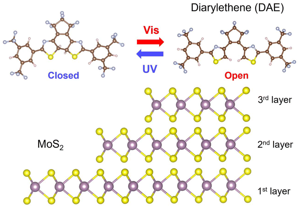 | ||
| Fig. 1 Schematic illustrating layer-number-dependent charge transfer interactions between MoS2 and DAE. UV and visible light trigger isomerization between the closed and the open form. UV irradiation results in a π-conjugated closed-form photoisomer, while visible light produces a cross-conjugated open-form. The photoisomerization changes the HOMO and LUMO levels of DAE. 1L, 2L, and 3L MoS2 can interact differently with DAE, leading to layer-number-dependent photoswitchability. | ||
 | ||
| Fig. 2 (a) Optical and (b) AFM images of 1L MoS2 indicated by dotted lines. (c) The AFM height profile shows that the thickness of the DAE layer is approximately 2 nm, while the monolayer MoS2 has a thickness of about 0.8 nm. (d)–(f) PL intensity of 1L, 2L, and 3L MoS2-DAE samples measured under alternating UV-visible irradiation. A 633 nm HeNe laser was used for excitation. (d) 1L MoS2 shows a drastic PL quenching after UV irradiation. However, the signal recovers fully under visible light. This photo-modulation is repeated three times. In contrast, no significant PL quenching is observed from the hybrids with (e) 2L and (f) 3L MoS2. | ||
We measured PL to probe interfacial charge transfer behaviors in the MoS2-DAE hybrids using a confocal Raman microscope. To explore wavelength-dependent photoswitchability, we initially exposed the samples to visible light (using a 530 nm long-pass filter) for 10 minutes to trigger DAE isomerization to the open isomeric form. After the exposure, we recorded the PL spectra using a 633 nm HeNe laser for excitation. Note that DAE molecules exhibit minimal absorbance at 633 nm.25 Subsequently, we irradiated the samples with UV light (∼312 nm) for 2 minutes to switch it to the closed form and compared the resulting PL intensities. The alternating UV-visible light exposure was performed three times, and the results are presented in Fig. 2d–f (also see Fig. S2†). The sharp Raman peak at ∼650 nm indicates the fingerprint of A1g band in MoS2, which is consistent with previous reports.33,34 Comparing the PL characteristics of 1L, 2L, and 3L MoS2, distinct patterns emerge. The 1L MoS2-DAE sample shows a distinct PL peak at approximately 660 nm, indicative of a direct bandgap. The PL peaks of 2L and 3L hybrids shift to about 670 and 680 nm, respectively. These layer-number-dependent PL emissions are in good agreement with the measurements in literature.35,36Fig. 2d shows a substantial PL quenching in 1L MoS2-DAE after UV irradiations. The emission signals are recovered after exposure to visible light. This behavior must be associated with DAE's isomeric forms since 1L MoS2 without a DAE layer does not show any significant differences between UV and visible irradiation (Fig. S3a†). It is attributed to photoinduced charge transfer at the hybrid interfaces that suppresses excitonic recombination of electron–hole pairs in MoS2. Three consecutive cycles of visible and UV exposure result in consistent PL quenching and recovery, in line with what is expected from robust photoswitching (no significant degradation in performance due to undesired formation of irreversible photo-products).37,38Fig. 2e and f displays no significant quenching effect in both 2L and 3L MoS2-DAE samples after each cycle. The experimental results suggest that the 1L MoS2-DAE hybrid experiences notable charge transfer interactions, while there are no such interactions between DAE molecules and 2L or 3L MoS2.
Next, bulk MoS2 crystals were mechanically exfoliated onto ITO glass to investigate the hybrids using C-AFM (Fig. S4†). The measurements were conducted by placing the samples between the ITO and Pt–Ir probe while applying a DC bias voltage of ±2 V. Fig. 3 and S5† present current vs. bias voltage plots of 1L–3L MoS2-DAE hybrids after light exposure. In Fig. 3a, 1L MoS2 with the closed-form DAE (after UV exposure) demonstrates significantly higher current than with the open-form isomers (after visible irradiation) at the same applied voltage. For example, approximately 7.12 nA was measured at 0.60 V after UV irradiation compared to ∼0.07 nA after exposure to visible light. It is thus evident that light conditions drastically influence the hybrid, and the conductivity of 1L MoS2 is greatly enhanced with closed-form DAE. It should be noted that the photo-modulation is not observed from MoS2 without DAE molecules (Fig. S3b†). The two different isomeric forms of DAE also change the threshold voltage significantly. It decreases from ∼0.50 V (open-form) to ∼0.14 V (closed-form) under positive potential and increases from ∼−0.60 V to ∼−0.30 V under negative potential. This could be due to either p- or n-doping effects. Either way, the number of majority carriers will increase, which will accordingly improve the conductivity and promote greater current flow under a given DC bias voltage.39
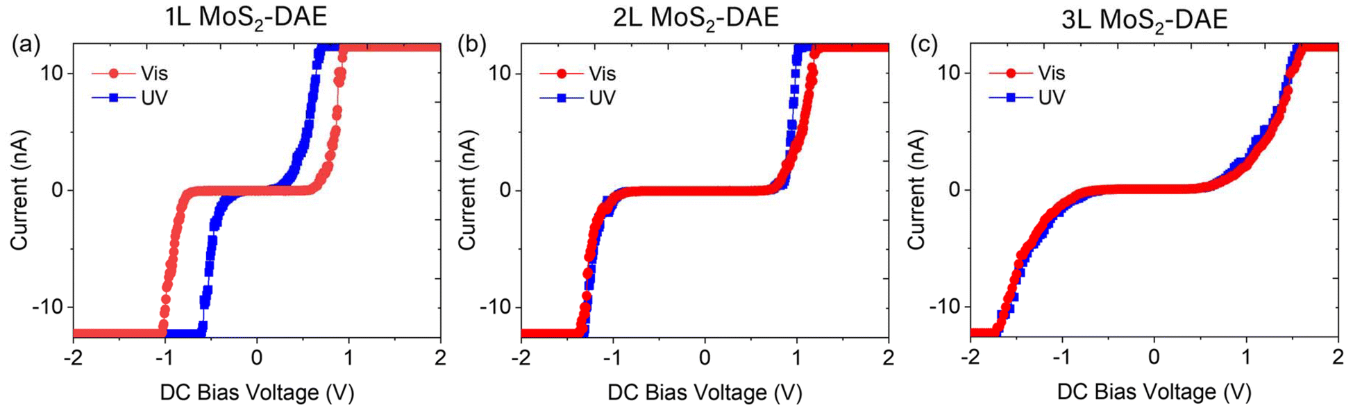 | ||
| Fig. 3 Conductive AFM measurements on photoswitched hybrid samples under UV and visible irradiation: (a) 1L MoS2-DAE, (b) 2L MoS2-DAE, and (c) 3L MoS2-DAE. Bias DC voltage was applied from −2 V to 2 V and currents were recorded within ±12 nA. UV light enhances the current significantly in 1L MoS2-DAE, whereas no significant changes are observed from the hybrids with 2L and 3L MoS2. | ||
In contrast, the C-AFM results of 2L and 3L MoS2-DAE samples in Fig. 3b and c show that there are no significant changes in current and conductivity after UV-induced isomerization from the DAE open-form to the closed-form. The small difference in current of 2L MoS2-DAE around 1 V DC bias voltage may be attributed to a local electric field effect, photothermal effect, or minor doping.1,40 Since only 1L hybrid demonstrated enhanced conductivity and current flow while 2L and 3L samples did not, we performed DFT calculations to elucidate potential doping mechanisms in 1L MoS2-DAE that account for the difference.
Densities of states (DOS) were obtained from DFT calculations for the 1L, 2L, and 3L MoS2-DAE hybrids as shown in Fig. 4 (also see Fig. S1†). The energy states of an isolated DAE photoisomer were calculated following the methodology from our previous work,25 setting the vacuum level to zero. DFT calculations have proven to be effective determining relative energy level alignments in 2D heterolayers.41,42 The structural transformation of DAE between its open and closed states leads to considerable shifts in the HOMO and LUMO levels. The closed-form DAE exhibits HOMO and LUMO energy levels of approximately −5.75 and −4.31 eV, respectively; around −6.32 and −3.80 eV are obtained with the open isomeric form. The gap between the HOMO and LUMO levels is ∼1.4 eV for closed-form isomer and ∼2.5 eV for open DAE, resulting in a gap change of around 1.1 eV. Thus, the energy level window becomes narrowed after UV irradiation.
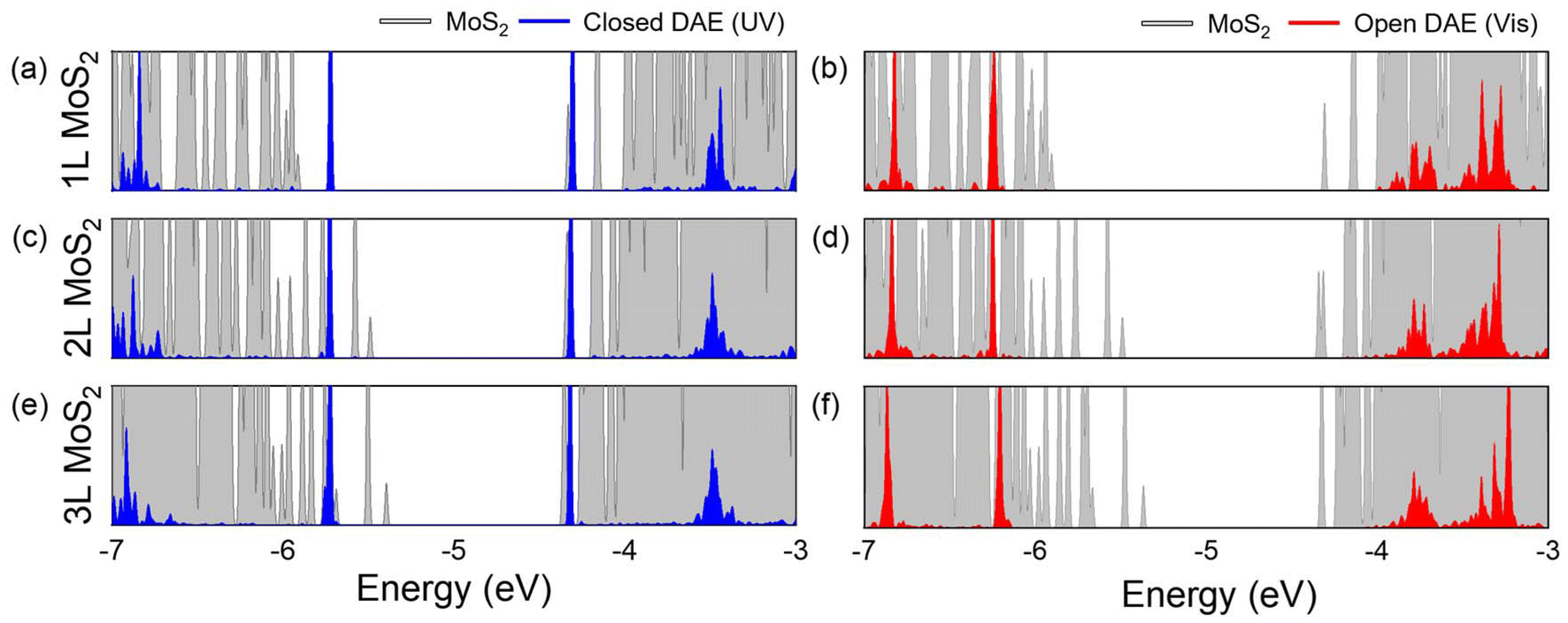 | ||
| Fig. 4 DFT-calculation of density of electronic states (DOS), showing the alignment of VBM and CBM energies of 1L–3L MoS2 with the HOMO and LUMO levels of closed- and open-form DAE under UV and visible light, respectively. The LUMO and HOMO levels of closed-form DAE are approximately −4.31 and −5.75 eV. In the open state, these values are around −3.80 and −6.32 eV, respectively. For closed-form DAE interacting with 1L MoS2 (a), its HOMO level is higher than the MoS2 VBM by approximately 0.16 eV. However, it is lower than the VBM levels of 2L and 3L MoS2 by about 0.26 eV (c) and 0.36 eV (e). From (b), (d), and (f), the LUMO level is slightly higher than the CBM energies of all 1L, 2L, 3L MoS2 by approximately 0.02–0.05 eV. In contrast, the HOMO level of open-form isomer is always lower than the MoS2 VBM energies, and the LUMO is significantly higher than the CBM of 1L, 2L, and 3L MoS2. | ||
It can be observed that the VBM level of MoS2 rises drastically as the layer number increases from 1L to 3L, while the CBM remains similar. The CBM of 1L, 2L, and 3L MoS2 are approximately −4.33, −4.34, and −4.36 eV, respectively; the VBM levels are about −5.91, −5.49, and −5.39 eV. Investigating the energy differences between LUMO and CBM and between HOMO and VBM is crucial for determining energetically favorable charge transfer mechanisms and identifying which carrier will be transferred between MoS2 and DAE. Electron transfer from MoS2 to DAE may occur if the DAE's LUMO is lower than the CBM of MoS2, and hole transfer will take place if the DAE's HOMO is higher than the VBM of MoS2.
For the hybrids with the closed-form DAE, the LUMO level is slightly higher than the CBM of 1L, 2L, and 3L MoS2 by approximately 0.02, 0.03, and 0.05 eV, respectively. Thus, there may not be a tendency of electron transfer from MoS2 to the closed DAE. The HOMO is higher than the VBM of 1L MoS2 by ∼0.16 eV, but it becomes lower than the VBMs of 2L and 3L MoS2 by 0.26 eV and 0.36 eV, respectively. This suggests the possible hole transfer to the closed DAE from 1L MoS2, but not from 2L or 3L MoS2. This hole transfer generates the doping effect in the 1L MoS2 flake.
In contrast, both the HOMO and LUMO levels of open-form DAE are outside the bandgap of all MoS2 layers as shown in Fig. 4b, d, and f. The HOMO level of the open-form isomer is always lower than the VBM of MoS2, while its LUMO is significantly higher than the CBM of 1L, 2L, and 3L MoS2 by about 0.53, 0.54, and 0.56 eV, respectively. Therefore, charge transfer from MoS2 layers to the open DAE isomers is unlikely.
The energy band diagram in Fig. 5 illustrates the fundamental mechanisms involved in MoS2-DAE hybrids based on DFT calculations. Since the LUMO levels of both the open and the closed isomeric forms of DAE are higher than the CBM levels of the MoS2 layers, electron transfer from MoS2 to DAE cannot take place. On the other hand, the HOMO level of closed-form DAE is higher than the VBM energy of 1L MoS2, which may facilitate the hole transfer from the 1L MoS2 to DAE. However, such transfer is unfavorable with 2L and 3L MoS2. Overall, the photoswitchable hole transfer is a dominant mechanism that quenches PL and enhances conductivity of 1L MoS2. Furthermore, there is a strong layer-number-dependence that alters the interactions between MoS2 and photochromic DAE molecules.
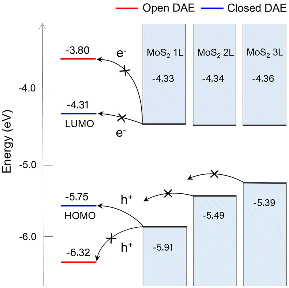 | ||
| Fig. 5 The energy diagrams of hybrid structures involving 1L to 3L MoS2 and DAE show the alignment of MoS2's CBM and VBM energies against the HOMO and LUMO levels of open- and closed-form DAE. In 1L MoS2, hole transfer from MoS2 to closed-form DAE is favorable since the HOMO is positioned higher than the CBM. In contrast, the CBM energies of 2L and 3L MoS2 are higher than the HOMO levels of both open and closed states, prohibiting hole transfer mechanisms. Photoinduced electron transfer is energetically not favored in all MoS2 configurations, because the CBM energies are lower than the LUMO of both open and closed DAE. | ||
This study is distinct and different from 1L MoSe2-DAE system in our previous report, where the interfacial interactions in the hybrid structure were dominated by electron transfer mechanisms.25 1L MoSe2 has a VBM that is higher than the HOMO of both open- and closed-form DAE by ∼0.97 eV and 0.40 eV, respectively. The CBM energy is approximately 0.05 eV lower than the LUMO level of open-form DAE while ∼0.46 eV higher than that of the corresponding closed isomer. This alignment facilitated electron transfer from the CBM of 1L MoSe2 to the LUMO of closed-ring DAE while suppressing any interaction with the open isomeric form. Another similar study was reported which studied electron transfer in few-layer WSe2 interfacing a different type of DAE.26 The report presented that the CBM of few-layer WSe2 (−3.5 eV) is higher than the LUMO of the closed form of DAE (−3.7 eV) but lower than that of the open form of DAE (−2.7 eV), resulting in electron charge transfer. In parallel, hole transfer has been observed in TMDs with organic layers. Huang and co-workers investigated interfacial charge transfer between 1L WS2 and a layer of tetracene molecules by using an ultrafast transient absorption method.43 When excited with a photon energy of ∼2.1 eV which is below tetracene's absorption edge, a hole transfer took place from the WS2 flake to tetracene. Building on these studies, our current work elucidates the layer-number-dependent photoswitchability in TMD-photochromic organic hybrid systems. We show that effective photo-modulated charge transfer in hybrid devices can be achieved by using DAE derivatives with energy levels specifically aligned to 2D semiconductors.
Conclusions
In this study, we demonstrated the effective photo-modulation of MoS2 flakes using DAE molecules. The interaction between DAE and MoS2 varies significantly with the number of MoS2 layers, as evidenced by PL and C-AFM measurements. Notably, monolayer MoS2-DAE displays significant PL quenching and increased conductivity after exposure to UV light (closed-ring isomers). DFT calculations support the observation showing that hole transfer is favorable in 1L MoS2 when interacting with the closed-form DAE. On the other hand, 2L and 3L MoS2 will not have any transfer interactions with DAE due to the energy level alignment.This work highlights the importance of precise layer control in developing optoelectronic devices and the potential of photoswitchable TMD devices. Our strategy may be extended to other 2D materials by utilizing other photochromic molecules (e.g., spiropyran and azobenzene) or a combination of multiple such molecules. A detailed understanding of interfacial interactions between TMDs and photochromic molecules will be required to design such systems. The photoswitchability and layer-number-dependence could open new possibilities for designing light-responsive nanoelectronics and optoelectronics. The advancements will usher in a new era of electronics, incorporating innovative functions within high-performing 2D materials toward light-driven technologies.
Materials and methods
Preparation of MoS2
Bulk MoS2 crystals (2D Semiconductors) were mechanically exfoliated onto cleaned p-doped SiO2/Si substrates and indium tin oxide glass (ITO, MTI KJ Group) using the Scotch tape method.44,45 They were subsequently heated on a hot plate at 50 °C for 10 or 30 minutes to enhance the adhesion of the exfoliated flakes. Before deposition, the SiO2/Si substrates were cleaned by ultrasonication in acetone, methanol, and deionized water (DI) for 15 minutes each to remove any contaminants or impurities from the surface. The residual fluids were blown off using compressed air, followed by soft baking on a hot plate at 110 °C for 5 minutes to ensure complete evaporation. The annealing process was conducted in a controlled Ar gas atmosphere at 250 °C for 1 hour to ensure optimal contact between the MoS2 flakes and the substrate, reduce surface contamination, enhance the quality of the interface, and improve the electronic properties.45–47Synthesis of DAE molecules
To synthesize the DAE compound, we followed a synthetic approach for the Negishi coupling reaction. This method was based on the Knochel modification48 and subsequent references,37 as recommended by previous reports.25,49 Briefly, we utilized 2,4-dibromo-5-methylthiazole and 3,5-bis(trifluoromethyl)-1-bromobenzene as reactants.25 This approach yielded 2-(3,5-bis(trifluoromethyl)phenyl)-4-bromo-5-methylthiophene as an intermediate product. The intermediate was converted in situ to the corresponding boronic pinacol ester, which was crucial for the Suzuki coupling reaction with 1,2-dichlorohexafluorocyclopent-1-ene, enabling the synthesis of the targeted DAE. The final DAE molecules were confirmed by nuclear magnetic resonance (NMR) measurement.25,50 They have zero absorption at 633 nm and do not exhibit fluorescent properties.25,51Functionalization of MoS2 with DAE
Both SiO2/Si substrates and ITO glass with MoS2 flakes were immersed in a DAE solution (0.02 mg mL−1 in chloroform) for 12 hours at 4 °C.26 After drying the DAE solution from the samples with compressed air, they underwent soft baking on a hot plate at 50 °C for 30 minutes. The photoswitching behaviors were studied by exposing the MoS2-DAE samples to UV light for 2 minutes, followed by exposure to visible light for 10 minutes. UV light was emitted by a Spectroline™ TE lamp at approximately 312 nm, while visible light was produced from a Xe-arc lamp with a 530 nm long-pass filter.Sample characterization
A Renishaw inVia Raman confocal microscope was used for MoS2 flake inspection and PL measurements with 10×, 20×, 50×, and 100× objective lenses. PL emissions were recorded using a 633 nm HeNe laser and a 100× objective lens. The layer numbers were first identified based on characteristic color contrasts caused by differences in transparency and interference effects33,47 and confirmed by AFM imaging. AFM and C-AFM were performed on both MoS2 and MoS2-DAE samples using the Bruker Dimension Icon AFM. Topological imaging to measure flake thickness utilized a SCANASYST-AIR probe, while an SCM-PIT-V2 probe was employed in C-AFM measurements. While measuring C-AFM, a current range of ±12 nA with a sensitivity of 1 nA V−1 was set, and bias voltage ranging from −2 V to 2 V was applied to avoid potential damage to both the probe tip and the samples.52DFT calculation
Vienna Ab initio Simulation Package (VASP) was used for DFT calculations with the projector augmented wave (PAW) method.53,54 To handle electron exchange and correlation, the Perdew–Burke–Ernzerhof (PBE) functional55 within the generalized gradient approximation was applied. The hybrid structures consisted of a DAE isomer placed on top of a (5 × 5) MoS2 slab as illustrated in Fig. S6.† A 14 Å vacuum layer was added. This setup resulted in an areal density of 4.5 × 10¹³ molecules per cm2. The MoS2 bi- and tri-layers were constructed with the AA′ type stacking order where the Mo(S) atom in one layer is aligned over the S(Mo) atom in the adjacent layer.56 To accurately model the van der Waals interactions between the MoS2 layers and the DAE, a dispersion correction was incorporated using the DFT-D2 method with Grimme.32 The electronic minimization was performed with a tolerance level of 10−5 eV. Ionic positions were relaxed until the Hellmann–Feynman forces were below 10 meV Å−1 with a 2 × 2 × 1 Γ-centered k-point mesh for the DAE-(5 × 5) MoS2 hybrid systems. After the ionic relaxation, a finer k-point mesh of 3 × 3 × 1 Γ-centered mesh was used for generating precise density of states.Data availability
The data supporting this article have been included as part of the ESI document.† Data are available upon request from the authors.Conflicts of interest
The authors declare no competing financial interest.Acknowledgements
This work was funded by the U.S. National Science Foundation under award no. 2151869 and 2151887.References
- Q. H. Wang, K. Kalantar-Zadeh, A. Kis, J. N. Coleman and M. S. Strano, Electronics and optoelectronics of two-dimensional transition metal dichalcogenides, Nat. Nanotechnol., 2012, 7, 699–712 CrossRef CAS PubMed.
- J. Yuan, S. Najmaei, Z. Zhang, J. Zhang, S. Lei, P. M. Ajayan, B. I. Yakobson and J. Lou, Photoluminescence quenching and charge transfer in artificial heterostacks of monolayer transition metal dichalcogenides and few-layer black phosphorus, ACS Nano, 2015, 9, 555–563 CrossRef CAS PubMed.
- D. Yang, S. J. Sandoval, W. Divigalpitiya, J. Irwin and R. Frindt, Structure of single-molecular-layer MoS 2, Phys. Rev. B: Condens. Matter Mater. Phys., 1991, 43, 12053 CrossRef CAS PubMed.
- V. Yadav, S. Roy, P. Singh, Z. Khan and A. Jaiswal, 2D MoS2−based nanomaterials for therapeutic, bioimaging, and biosensing applications, Small, 2019, 15, 1803706 CrossRef PubMed.
- X. Zhuang, Y. Mai, D. Wu, F. Zhang and X. Feng, Two–dimensional soft nanomaterials: a fascinating world of materials, Adv. Mater., 2015, 27, 403–427 CrossRef CAS PubMed.
- S. Balendhran, S. Walia, H. Nili, J. Z. Ou, S. Zhuiykov, R. B. Kaner, S. Sriram, M. Bhaskaran and K. Kalantar–zadeh, Two–dimensional molybdenum trioxide and dichalcogenides, Adv. Funct. Mater., 2013, 23, 3952–3970 CrossRef CAS.
- K. F. Mak, C. Lee, J. Hone, J. Shan and T. F. Heinz, Atomically thin MoS 2: a new direct-gap semiconductor, Phys. Rev. Lett., 2010, 105, 136805 CrossRef PubMed.
- D. Jariwala, V. K. Sangwan, L. J. Lauhon, T. J. Marks and M. C. Hersam, Emerging device applications for semiconducting two-dimensional transition metal dichalcogenides, ACS Nano, 2014, 8, 1102–1120 CrossRef CAS PubMed.
- M. Naqi, M. Kaniselvan, S. Choo, G. Han, S. Kang, J. Kim, Y. Yoon and S. Kim, Ultrasensitive multilayer MoS2−based photodetector with permanently grounded gate effect, Adv. Electron. Mater., 2020, 6, 1901256 CrossRef CAS.
- H. Kwon, P. J. Jeon, J. S. Kim, T.-Y. Kim, H. Yun, S. W. Lee, T. Lee and S. Im, Large scale MoS2 nanosheet logic circuits integrated by photolithography on glass, 2D Mater., 2016, 3, 044001 CrossRef.
- S. Barua, H. S. Dutta, S. Gogoi, R. Devi and R. Khan, Nanostructured MoS2-based advanced biosensors: a review, ACS Appl. Nano Mater., 2017, 1, 2–25 CrossRef.
- Z. Yu, Z. Y. Ong, S. Li, J. B. Xu, G. Zhang, Y. W. Zhang, Y. Shi and X. Wang, Analyzing the carrier mobility in transition–metal dichalcogenide MoS2 field–effect transistors, Adv. Funct. Mater., 2017, 27, 1604093 CrossRef.
- J. Lin, J. Zhong, S. Zhong, H. Li, H. Zhang and W. Chen, Modulating electronic transport properties of MoS2 field effect transistor by surface overlayers, Appl. Phys. Lett., 2013, 103, 063109 CrossRef.
- S. Aftab, Samiya, H. M. Ul Haq, S. Yousuf, M. U. Khan, Z. Ahmed, J. Aziz, M. W. Iqbal, A. ur Rehman and M. Z. Iqbal, van der Waals multi–heterostructures (PN, PIN, and NPN) for dynamic rectification in 2D materials, Adv. Mater. Interfaces, 2020, 7, 2001479 CrossRef CAS.
- K. S. Novoselov, A. Mishchenko, A. Carvalho and A. H. Castro Neto, 2D materials and van der Waals heterostructures, Science, 2016, 353, aac9439 CrossRef CAS PubMed.
- J. Ji and J. H. Choi, Layer–number–dependent electronic and optoelectronic properties of 2D WSe2–organic hybrid heterojunction, Adv. Mater. Interfaces, 2019, 6, 1900637 CrossRef.
- F. Pizzocchero, L. Gammelgaard, B. S. Jessen, J. M. Caridad, L. Wang, J. Hone, P. Bøggild and T. J. Booth, The hot pick-up technique for batch assembly of van der Waals heterostructures, Nat. Commun., 2016, 7, 11894 CrossRef CAS PubMed.
- X. Yang and M. Yan, Removing contaminants from transferred CVD graphene, Nano Res., 2020, 13, 599–610 CrossRef CAS.
- J. Ji and J. H. Choi, Recent progress in 2D hybrid heterostructures from transition metal dichalcogenides and organic layers: Properties and applications in energy and optoelectronics fields, Nanoscale, 2022, 14, 10648–10689 RSC.
- Y. L. Huang, Y. J. Zheng, Z. Song, D. Chi, A. T. Wee and S. Y. Quek, The organic–2D transition metal dichalcogenide heterointerface, Chem. Soc. Rev., 2018, 47, 3241–3264 RSC.
- M. Irie, T. Fukaminato, K. Matsuda and S. Kobatake, Photochromism of diarylethene molecules and crystals: memories, switches, and actuators, Chem. Rev., 2014, 114, 12174–12277 CrossRef CAS PubMed.
- F. A. Jerca, V. V. Jerca and R. Hoogenboom, Advances and opportunities in the exciting world of azobenzenes, Nat. Rev. Chem., 2022, 6, 51–69 CrossRef PubMed.
- R. Klajn, Spiropyran-based dynamic materials, Chem. Soc. Rev., 2014, 43, 148–184 RSC.
- C. L. Fleming, S. Li, M. Grøtli and J. Andréasson, Shining new light on the spiropyran photoswitch: a photocage decides between cis–trans or spiro-merocyanine isomerization, J. Am. Chem. Soc., 2018, 140, 14069–14072 CrossRef CAS PubMed.
- S. Park, J. Ji, C. Cunningham, S. Pillai, J. Rouillon, C. Benitez-Martin, M. Fang, E. H. Yang, J. Andreasson, J. H. You and J. H. Choi, Photoswitchable optoelectronic properties of 2D MoSe2/Diarylethene hybrid structures, Sci. Rep., 2024, 14, 7325 CrossRef CAS PubMed.
- H. Qiu, Y. Zhao, Z. Liu, M. Herder, S. Hecht and P. Samorì, Modulating the Charge Transport in 2D Semiconductors via Energy–Level Phototuning, Adv. Mater., 2019, 31, 1903402 CrossRef PubMed.
- M. Gobbi, S. Bonacchi, J. X. Lian, A. Vercouter, S. Bertolazzi, B. Zyska, M. Timpel, R. Tatti, Y. Olivier, S. Hecht, M. V. Nardi, D. Beljonne, E. Orgiu and P. Samorì, Collective molecular switching in hybrid superlattices for light-modulated two-dimensional electronics, Nat. Commun., 2018, 9, 2661 CrossRef PubMed.
- Y. Zhao, S. Ippolito and P. Samori, Functionalization of 2D Materials with Photosensitive Molecules: From Light–Responsive Hybrid Systems to Multifunctional Devices, Adv. Opt. Mater., 2019, 7, 1900286 CrossRef.
- C. Lee, H. Yan, L. E. Brus, T. F. Heinz, J. Hone and S. Ryu, Anomalous lattice vibrations of single-and few-layer MoS2, ACS Nano, 2010, 4, 2695–2700 CrossRef CAS PubMed.
- Y. Zhang, J. Ye, Y. Matsuhashi and Y. Iwasa, Ambipolar MoS2 thin flake transistors, Nano Lett., 2012, 12, 1136–1140 CrossRef CAS PubMed.
- T. Zheng, P. Valencia-Acuna, P. Zereshki, K. M. Beech, L. Deng, Z. Ni and H. Zhao, Thickness-dependent interlayer charge transfer in MoSe2/MoS2 heterostructures studied by femtosecond transient absorption measurements, ACS Appl. Mater. Interfaces, 2021, 13, 6489–6495 CrossRef CAS PubMed.
- S. Grimme, Semiempirical GGA–type density functional constructed with a long–range dispersion correction, J. Comput. Chem., 2006, 27, 1787–1799 CrossRef CAS PubMed.
- J. Ji, C. M. Delehey, D. N. Houpt, M. K. Heighway, T. Lee and J. H. Choi, Selective chemical modulation of interlayer excitons in atomically thin heterostructures, Nano Lett., 2020, 20, 2500–2506 CrossRef CAS PubMed.
- H. Li, Q. Zhang, C. C. R. Yap, B. K. Tay, T. H. T. Edwin, A. Olivier and D. Baillargeat, From bulk to monolayer MoS2: evolution of Raman scattering, Adv. Funct. Mater., 2012, 22, 1385–1390 CrossRef CAS.
- S. Mouri, Y. Miyauchi and K. Matsuda, Tunable photoluminescence of monolayer MoS2 via chemical doping, Nano Lett., 2013, 13, 5944–5948 CrossRef CAS PubMed.
- J. Shi, P. Yu, F. Liu, P. He, R. Wang, L. Qin, J. Zhou, X. Li, J. Zhou and X. Sui, 3R MoS2 with broken inversion symmetry: a promising ultrathin nonlinear optical device, Adv. Mater., 2017, 29, 1701486 CrossRef PubMed.
- M. Herder, B. M. Schmidt, L. Grubert, M. Pätzel, J. Schwarz and S. Hecht, Improving the fatigue resistance of diarylethene switches, J. Am. Chem. Soc., 2015, 137, 2738–2747 CrossRef CAS PubMed.
- L. Hou, R. Ringström, A. B. Maurer, M. Abrahamsson, J. Andréasson and B. Albinsson, Optically Switchable NIR Photoluminescence of PbS Semiconducting Nanocrystals using Diarylethene Photoswitches, J. Am. Chem. Soc., 2022, 144, 17758–17762 CrossRef CAS PubMed.
- S. Zhang, H. M. Hill, K. Moudgil, C. A. Richter, A. R. Hight Walker, S. Barlow, S. R. Marder, C. A. Hacker and S. J. Pookpanratana, Controllable, wide–ranging n–doping and p–doping of monolayer group 6 transition–metal disulfides and diselenides, Adv. Mater., 2018, 30, 1802991 CrossRef PubMed.
- W. Sakong, H. Z. Gul, B. Ahn, S. Oh, G. Kim, E. Sim, J. Bahng, H. Yi, M. Kim and M. Yun, Optical duality of molybdenum disulfide: metal and semiconductor, Nano Lett., 2022, 22, 5207–5213 CrossRef CAS PubMed.
- J. Kunstmann, F. Mooshammer, P. Nagler, A. Chaves, F. Stein, N. Paradiso, G. Plechinger, C. Strunk, C. Schüller and G. Seifert, Momentum-space indirect interlayer excitons in transition-metal dichalcogenide van der Waals heterostructures, Nat. Phys., 2018, 14, 801–805 Search PubMed.
- R. Besse, J. F. Silveira, Z. Jiang, D. West, S. Zhang and J. L. Da Silva, Beyond the Anderson rule: importance of interfacial dipole and hybridization in van der Waals heterostructures, 2D Mater., 2021, 8, 041002 Search PubMed.
- T. Zhu, L. Yuan, Y. Zhao, M. Zhou, Y. Wan, J. Mei and L. Huang, Highly mobile charge-transfer excitons in two-dimensional WS2/tetracene heterostructures, Sci. Adv., 2018, 4, eaao3104 Search PubMed.
- S. Park, J. Ha, M. F. Khan, C. Im, J. Y. Park, S. H. Yoo, M. A. Rehman, K. Kang, S. H. Lee and S. C. Jun, Pronounced Optoelectronic Effect in n–n ReS2 Homostructure, ACS Appl. Electron. Mater., 2022, 4, 4306–4315 Search PubMed.
- J. Ji and J. H. Choi, Understanding the Effects of Dielectric Property, Separation Distance, and Band Alignment on Interlayer Excitons in 2D Hybrid MoS2/WSe2 Heterostructures, ACS Appl. Electron. Mater., 2021, 3, 3052–3059 Search PubMed.
- J. Choi, H. Zhang, H. Du and J. H. Choi, Understanding solvent effects on the properties of two-dimensional transition metal dichalcogenides, ACS Appl. Mater. Interfaces, 2016, 8, 8864–8869 CrossRef CAS PubMed.
- H. Zhang, J. Ji, A. A. Gonzalez and J. H. Choi, Tailoring photoelectrochemical properties of semiconducting transition metal dichalcogenide nanolayers with porphyrin functionalization, J. Mater. Chem. C, 2017, 5, 11233–11238 RSC.
- S. Sase, M. Jaric, A. Metzger, V. Malakhov and P. Knochel, One-pot Negishi cross-coupling reactions of in situ generated zinc reagents with aryl chlorides, bromides, and triflates, J. Org. Chem., 2008, 73, 7380–7382 CrossRef CAS PubMed.
- G. Naren, W. Larsson, C. Benitez-Martin, S. Li, E. Pérez-Inestrosa, B. Albinsson and J. Andréasson, Rapid amplitude-modulation of a diarylethene photoswitch: en route to contrast-enhanced fluorescence imaging, Chem. Sci., 2021, 12, 7073–7078 RSC.
- C.-W. Hsu, C. Sauvée, H. Sundén and J. Andréasson, Writing and erasing multicolored information in diarylethene-based supramolecular gels, Chem. Sci., 2018, 9, 8019–8023 RSC.
- L. Hou, W. Larsson, S. Hecht, J. Andréasson and B. Albinsson, A general approach for all-visible-light switching of diarylethenes through triplet sensitization using semiconducting nanocrystals, J. Mater. Chem. C, 2022, 10, 15833–15842 RSC.
- J. Choi, H. Zhang and J. H. Choi, Modulating optoelectronic properties of two-dimensional transition metal dichalcogenide semiconductors by photoinduced charge transfer, ACS Nano, 2016, 10, 1671–1680 CrossRef CAS PubMed.
- G. Kresse and J. Furthmüller, Efficient iterative schemes for ab initio total-energy calculations using a plane-wave basis set, Phys. Rev. B: Condens. Matter Mater. Phys., 1996, 54, 11169 CrossRef CAS PubMed.
- G. Kresse and D. Joubert, From ultrasoft pseudopotentials to the projector augmented-wave method, Phys. Rev. B: Condens. Matter Mater. Phys., 1999, 59, 1758 CrossRef CAS.
- J. P. Perdew, K. Burke and M. Ernzerhof, Generalized gradient approximation made simple, Phys. Rev. Lett., 1996, 77, 3865 CrossRef CAS PubMed.
- J. He, K. Hummer and C. Franchini, Stacking effects on the electronic and optical properties of bilayer transition metal dichalcogenides MoS2, MoSe2, WS2, and WSe2, Phys. Rev. B: Condens. Matter Mater. Phys., 2014, 89, 075409 CrossRef.
Footnote |
| † Electronic supplementary information (ESI) available. See DOI: https://doi.org/10.1039/d4nr03631j |
| This journal is © The Royal Society of Chemistry 2025 |