
 Open Access Article
 This Open Access Article is licensed under a Creative Commons Attribution-Non Commercial 3.0 Unported Licence
Intrinsic setting of the exciton state in MoS2 monolayers via tailoring the Moiré correlation with a sapphire substrate†
Chun-Wen
Chan
a,
Fang-Mei
Chan
a,
Sheng-Kuei
Chiu
bc,
Lu-Chih
Chen
c,
Wun-Jhen
Yu
a,
Chia-Yun
Hsieh
a and
Chao-Yao
Yang
 *ad
*ad
aDepartment of Materials Science and Engineering, National Yang Ming Chiao Tung University, Hsinchu, 300093, Taiwan. E-mail: cyyang8611@nycu.edu.tw
bDepartment of Materials Science, National University of Tainan, Tainan 70005, Taiwan
cDepartment of Materials Science and Engineering, Feng Chia University, Taichung City, 407102, Taiwan
dCenter for Emergent Functional Matter Science, National Yang Ming Chiao Tung University, Hsinchu 300093, Taiwan
First published on 11th February 2025
Abstract
This study aims to elucidate the specific Moiré correlation and associated exciton properties within MoS2 monolayers grown randomly oriented on a c-cut single-crystalline sapphire (Al2O3) substrate, which facilitates a distinct Moiré correlation. Notably, the exciton state in MoS2 monolayers appeared periodically linked to the stacking geometry with the sapphire substrate. Specifically, the observed stacking configuration of MoS2[11![[2 with combining macron]](https://www.rsc.org/images/entities/char_0032_0304.gif) 0]/Al2O3[110] induced a redshifted exciton state, while a 30-degree-misaligned stacking, such as MoS2[110]/Al2O3[01
0]/Al2O3[110] induced a redshifted exciton state, while a 30-degree-misaligned stacking, such as MoS2[110]/Al2O3[01![[1 with combining macron]](https://www.rsc.org/images/entities/char_0031_0304.gif) 0], increased the exciton energy. The variation in the exciton state due to changes in the stacking geometry between MoS2 and sapphire thus exhibited a 6-fold periodicity, reflecting the combination of hexagonal MoS2 and the trigonal sapphire substrate. This transition in the exciton state of the MoS2 monolayer was attributed to stacking-induced strain: the MoS2[110]/Al2O3[110] stack resulted in a closely packed nature with induced tensile strain in the film plane, whereas the MoS2[110]/Al2O3[010] stack appeared lightly packed, thus rendering the MoS2 structurally relaxed. These findings regarding the stacking-induced strain issues are consistent with the results of Raman spectra. This work underscores the potential for manipulating the crystallographic stacking between single-crystalline MoS2 monolayers and sapphire substrates to serve as a versatile platform for investigating photonics in MoS2-based heterostructures.
0], increased the exciton energy. The variation in the exciton state due to changes in the stacking geometry between MoS2 and sapphire thus exhibited a 6-fold periodicity, reflecting the combination of hexagonal MoS2 and the trigonal sapphire substrate. This transition in the exciton state of the MoS2 monolayer was attributed to stacking-induced strain: the MoS2[110]/Al2O3[110] stack resulted in a closely packed nature with induced tensile strain in the film plane, whereas the MoS2[110]/Al2O3[010] stack appeared lightly packed, thus rendering the MoS2 structurally relaxed. These findings regarding the stacking-induced strain issues are consistent with the results of Raman spectra. This work underscores the potential for manipulating the crystallographic stacking between single-crystalline MoS2 monolayers and sapphire substrates to serve as a versatile platform for investigating photonics in MoS2-based heterostructures.
1. Introduction
Transition-metal dichalcogenides (TMDs) in the form of monolayers have sparked significant interest due to their unique physical properties.1–3 These properties include optics,4–6 electrical transport,2,7 piezoelectricity,8,9 and valley spintronics,10,11 driving advancements in two-dimensional (2D) semiconductor technologies. Photonics is a crucial area of studying TMD monolayers, given their direct bandgap,9 which expands the possibilities for semiconductor applications in visible-light (VL)-based photonics.12,13 Moreover, the sensitivity of TMD monolayers to VL makes them suitable for characterization using VL-based spectroscopic techniques such as Raman and photoluminescence (PL) spectroscopy using lasers of 633 nm or 532 nm. In the emerging field of twistronics, it has been demonstrated that combining two TMD monolayers with specific crystallographic geometry can produce diverse Moiré patterns based on bilayer stacking, leading to significant changes in the properties of TMDs.14–16 Twistronics explores how the packing of two TMD monolayers influences the formation of Moiré patterns, offering insights into ex situ treatments for enhancing or modifying TMD properties. It also provides a new dimension to tailor TMDs to fit various facets of application. However, an important yet overlooked aspect of twistronics is the growth of TMD monolayers on a single-crystalline substrate with specific stacking geometry. Understanding the pseudo-Moiré correlation in TMD monolayers on single-crystalline substrates is crucial for establishing a strong interaction between physical properties and stacking geometry, mirroring the current focus on twistronics but presenting an unresolved challenge.This study attempts to explore the effect of the stacking geometry, as well as the Moiré correlation, of an MoS2 monolayer grown on a c-cut single-crystalline sapphire (Al2O3) substrate using a chemical vapor deposition technique. Without the pre-treatments utilizing annealing for establishing atomic steps on the sapphire surface before deposition,17,18 the synthesized MoS2 monolayers appeared to be randomly orientated on the sapphire surface, providing a unique playground to study the variation of the photonics properties of MoS2 monolayers arising from the specific Moiré pattern via layer stacking. This work would give another insight into the current twistronics and may pave an avenue toward structurally tailorable 2D device technologies.
2. Experimental
MoS2 monolayers were grown by using a chemical vapor deposition (CVD) technique in a 3-temperature-zone furnace, in which the sulfur powders (Alfa Aesar, 99.5%) of 0.3 g were placed at the edge of zone 1, MoO3 powders (Alfa Aesar, 99.95%) of 2 mg were placed at zone 2, and the sapphire substrates with c-cut surface were positioned 7 cm downstream from the MoO3 source at zone 3. Before CVD, the furnace was purged using an Ar flow for three consecutive cycles to maintain a contamination-free environment in the beginning. After the Ar purging, the temperatures at zones 1, 2, and 3 were ramped up to 550, 750, and 850 °C, respectively, in 90 minutes. The sulfur powders were subsequently heated up to 200 °C to supply the sulfur vapors interacting with MoO3 vapors at zone 2. During the experiment, an Ar carrier gas of 100 sccm was applied throughout the process to carry the hybrid S/MoO3 atmosphere to zone 3 and then the deposition on the surface of sapphire substrates was carried on for 15 minutes. Finally, the samples were cooled down to room temperature in the furnace for approximately 2 hours. The morphology of MoS2 monolayers was pictured using an optical microscope to examine the domain orientations on a sapphire substrate as shown in Fig. 1(a). The Raman and photoluminescence spectra were acquired using a Raman spectroscopy system with an argon laser source of 533 nm at room temperature. The laser beam was focused onto the sample's surface and the spot size was approximately 1 μm. The continuous-wave (CW) laser power was 75 mW, and a 1200 line per mm grating was employed for an energy resolution of 2 meV. The integration time for collecting Raman and PL spectra was 30 and 5 seconds to yield distinguishable signals, respectively. All the PL and Raman spectra were acquired from the samples at 298 K under the atmosphere.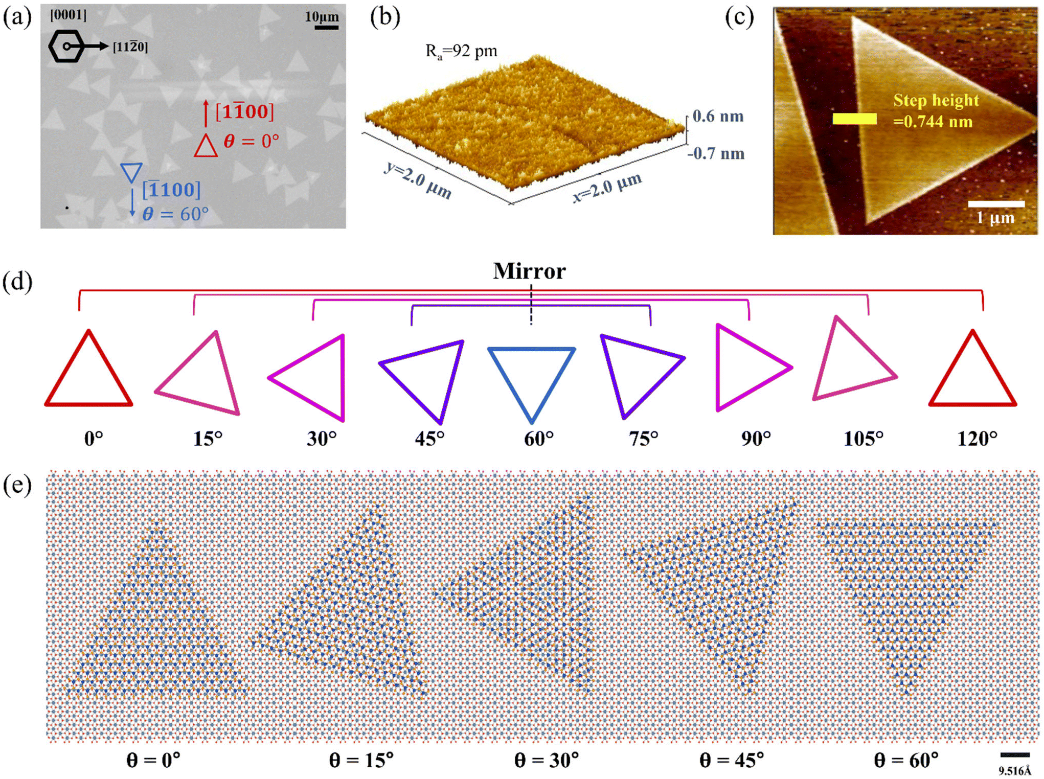 | ||
| Fig. 1 (a) Optical microscopy image of MoS2 monolayers distributed on the sapphire substrate with well-defined crystallographic orientations. (b) Atomic force microscopy image showing the surface roughness of the bare Al2O3 substrate employed in this study. The roughness (Ra) is approximately 92 pm as an atomically flat condition for studying the Moiré correlation in the MoS2/Al2O3 stack. (c) Atomic force microscopy image showing the MoS2/Al2O3 stack, in which the step height of MoS2 is 0.744 nm, corresponding to the thickness of the monolayer. (d) θ-Dependence and the periodicity of MoS2 monolayers defined via the distribution in (a), in which θ = 0° stands for aligning MoS2[100]/Al2O3[100]. θ = 15° and 45° are crystallographically identical to θ = 75° and 105°, respectively, due to their mirror stacking geometry in both hexagonal lattices. (e) The simulated Moiré patterns upon growing MoS2 monolayers on sapphire with various θ. The simulated patterns are obtained using Vesta software. | ||
3. Results
The MoS2 monolayers (space group: P![[6 with combining macron]](https://www.rsc.org/images/entities/char_0036_0304.gif) m2, a = b = 3.19214 Å and c = 13.37829 Å)19 grown on a c-cut single crystalline sapphire (Al2O3, space group: R
m2, a = b = 3.19214 Å and c = 13.37829 Å)19 grown on a c-cut single crystalline sapphire (Al2O3, space group: R![[3 with combining macron]](https://www.rsc.org/images/entities/char_0033_0304.gif) C, a = b = 4.75815 Å and c = 12.98970 Å)20 substrate investigated in this study are randomly orientated, as shown in Fig. 1(a). Fig. 1(a) also defines the crystallographic correlation between MoS2 monolayers and the sapphire substrate, in which we assign the stacking angle (θ) = 0° for the alignment through MoS2[100]/Al2O3[100], as labeled in Fig. 1(a). The sapphire substrate utilized in this work was atomically flat with a surface roughness of ∼92 pm as shown in Fig. 1(b). Fig. 1(c) shows the atomic force microscopy image of the sharp edge of the MoS2 domain, verifying the step height of the monolayer of ∼0.744 nm. In Fig. 1(a), the MoS2 monolayers with varying θ rotating clockwise can be observed on the atomically flat sapphire substrate, which may be due to the growth mechanisms lacking preferred nucleation sites during the chemical vapor deposition.21,22Fig. 1(d) demonstrates the correlation of the varying θ in reference to the crystallography of the sapphire substrate. It should be noted that the period of the varied θ shows a 6-fold symmetry based on the crystallographic correlation between MoS2 monolayers and the sapphire substrate. Therefore, the resulting stacking patterns are demonstrated in Fig. 1(e), in which the pattern appears to be in a 6-fold periodicity, providing a model system to use spectroscopy to resolve the effect of stacking geometry.
C, a = b = 4.75815 Å and c = 12.98970 Å)20 substrate investigated in this study are randomly orientated, as shown in Fig. 1(a). Fig. 1(a) also defines the crystallographic correlation between MoS2 monolayers and the sapphire substrate, in which we assign the stacking angle (θ) = 0° for the alignment through MoS2[100]/Al2O3[100], as labeled in Fig. 1(a). The sapphire substrate utilized in this work was atomically flat with a surface roughness of ∼92 pm as shown in Fig. 1(b). Fig. 1(c) shows the atomic force microscopy image of the sharp edge of the MoS2 domain, verifying the step height of the monolayer of ∼0.744 nm. In Fig. 1(a), the MoS2 monolayers with varying θ rotating clockwise can be observed on the atomically flat sapphire substrate, which may be due to the growth mechanisms lacking preferred nucleation sites during the chemical vapor deposition.21,22Fig. 1(d) demonstrates the correlation of the varying θ in reference to the crystallography of the sapphire substrate. It should be noted that the period of the varied θ shows a 6-fold symmetry based on the crystallographic correlation between MoS2 monolayers and the sapphire substrate. Therefore, the resulting stacking patterns are demonstrated in Fig. 1(e), in which the pattern appears to be in a 6-fold periodicity, providing a model system to use spectroscopy to resolve the effect of stacking geometry.
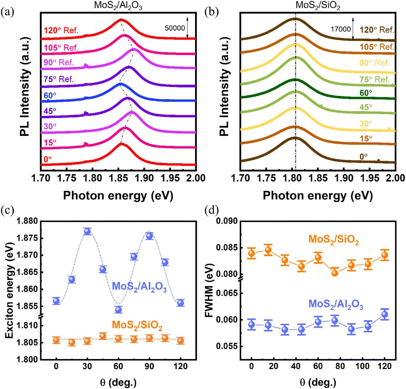
Fig. 2(a) and (b) display the θ-dependent PL spectra of MoS2 monolayers on the Al2O3 and SiO2 substrates, respectively. Note that the SiO2 utilized is an amorphous substrate and herein MoS2[100]/Si[100] is set as θ = 0° for a reference to verify the θ-dependence in the MoS2/Al2O3 stack. Consequently, both systems feature the exciton state in MoS2, which serves as a spectroscopic signature of the monolayer. However, the θ-dependent PL spectra acquired from the MoS2/Al2O3 stack show significant 6-fold periodicity as indicated by the dashed line as a guide to the eye. In contrast, this 6-fold periodicity does not appear in the MoS2/SiO2 heterostructure. Note that all the PL spectra were acquired at the center of MoS2 domains to eliminate the effects of structural imperfection in the vicinity of the edge (see ESI 1†). In order to clearly demonstrate the 6-fold periodicity in the MoS2/Al2O3 stack, Fig. 2(c) displays the plots of the exciton energy versus the change of θ for the MoS2/Al2O3 stack alongside the results taken from the MoS2/SiO2 stack, and their full width at half maximum (FWHM) is shown in Fig. 2(d). The former follows an ideal 6-fold periodicity as expected from the schematic diagram in Fig. 1(e) and the 6-fold periodicity vanishing in the latter case should be attributed to the amorphous nature of SiO2, giving rise to the absence of crystallographic correlation while stacking. It could be noticed that the FWHM is less sensitive to the θ dependence and is nearly constant for both cases; therefore, the observed PL shifting may be attributed to the band structural modification rather than the n-doping associated transition, i.e. exciton to trion.23,24 In addition to the vanished 6-fold periodicity, the redshifted exciton of MoS2 on SiO2 (to ∼1.805 eV) was observed, which might be attributed to the transition from exciton to trion as a result of the extra n-doping effect as observed in the CVD-grown MoS2 on the SiO2 substrate relative to sapphire.25,26 Besides, the broadening PL FWHM taken from the MoS2/SiO2 stack may also reveal the exciton to trion transition and superimposition accompanying the n-doping effect.25,26 Again, the data of θ > 60° were selected for arbitrary references because those are crystallographically repeated as conceptually demonstrated in Fig. 1(d) and (e).
 | ||
| Fig. 2
θ-Dependent PL spectra acquired from the (a) MoS2/Al2O3 and (b) MoS2/SiO2 stacks. Note: the spectra in (a) and (b) taken for θ = 75, 90, and 105 degrees are arbitrarily selected to extend the 6-fold correlation for a clear comparison, and signals at approximately 1.785 eV in (a) correspond to the Raman response of the Al2O3 substrate and are independent of varying θ. (c) Changes of exciton energy as a function of θ acquired from the MoS2/Al2O3 and MoS2/SiO2 stacks as the representatives for the well-defined crystallographic correlation and the absent structural correlation, respectively. Herein, the θ = 0° of the MoS2/SiO2 stack is defined by aligning MoS2[100]/Si[100]. (d) Full width at half maximum (FWHM) of PL spectra as a function of θ acquired from the MoS2/Al2O3 and MoS2/SiO2 stacks. The error bars in (c) and (d) were determined by the energy resolution of PL spectroscopy ∼2 meV. The PL spectra were acquired using a Raman spectroscopy system with an argon CW laser source of 533 nm of 75 mW at room temperature under the atmosphere. | ||
Based on the results in Fig. 2(a) and (b), it has been shown that the exciton state in MoS2 monolayers was highly correlated with θ in the MoS2/Al2O3 stack, namely the Moiré correlation between MoS2 monolayers and the Al2O3 substrate. While revisiting the θ-dependent Raman spectra of the MoS2/Al2O3 and MoS2/SiO2 stacks shown in Fig. 3(a) and (b), respectively, a similar 6-fold periodicity can be observed in MoS2/Al2O3 and is also absent in MoS2/SiO2. Fig. 3(c) and (d) present the plots of the A1g and E12g state of MoS2 for the cases of MoS2/Al2O3 and MoS2/SiO2, respectively, in which the wave number differences (Δk) between E12g and A1g are all approximately 20 cm−1, which stands for the fingerprint of the MoS2 monolayer.25,26 However, it can be seen that both the E12g and A1g states were stiffened while the θ deviates from the 0°/60° correlation in the MoS2/Al2O3 stack, and reach the maximum wave number value while θ reaches the 30°-associated counterparts, as shown in Fig. 3(c) and (d). According to the previous literature, the spontaneous Raman shifting on the A1g state is correlated with the n-doping effect led by charge-transfer from the substrates26,27 or the gating,28 which echoes the exciton to trion transition on the PL results in Fig. 2(c). On the counterpart, Raman softening on the E12g state may be attributed to the isotropic tensile stress of the MoS2 monolayers in the plane,29 which may structurally result from the preferred atomic population during the growth of MoS2 on the sapphire substrate, as reported in the epitaxially grown heterostructures, such as at the pyramid top sites on the substrate.30,31 The softened E12g state of MoS2 on SiO2 may be attributed to the isotropic tensile strain embedded during CVD growth, which is absent in the exfoliated MoS2 on SiO2 as demonstrated in the supporting information of A. Michail et al.'s study.26Fig. 4 series demonstrates the simulated MoS2/Al2O3 stack for examining the θ dependence, in which the 0°/60° correlation (Fig. 4(a)) can always promote the S atoms at the bottom surface of MoS2 to populate at the valley site among O atoms, suggesting the closely packed configuration at the MoS2/Al2O3 interface. Therefore, the closely packed nature may give rise to the isotropic tensile stress and reduce the van der Waals gap distance accordingly. In contrast, for the misaligned cases such as the θ = 15° (Fig. 4(b)) or θ = 30° correlation (Fig. 4(c)), it can be seen that the S atoms are partially superimposed with O atoms from the top-view images, especially for θ = 30°, as highlighted by the blue spots. The result suggests that partial S atoms may populate directly on top of O atoms, hence generally giving rise to the longer van der Waals gap distance and reducing the horizontal tensile strain, conceptually demonstrated in ESI 2.† Both results echo the Raman stiffening at the E12g and A1g states while the θ deviates from the 0°/60° correlation.
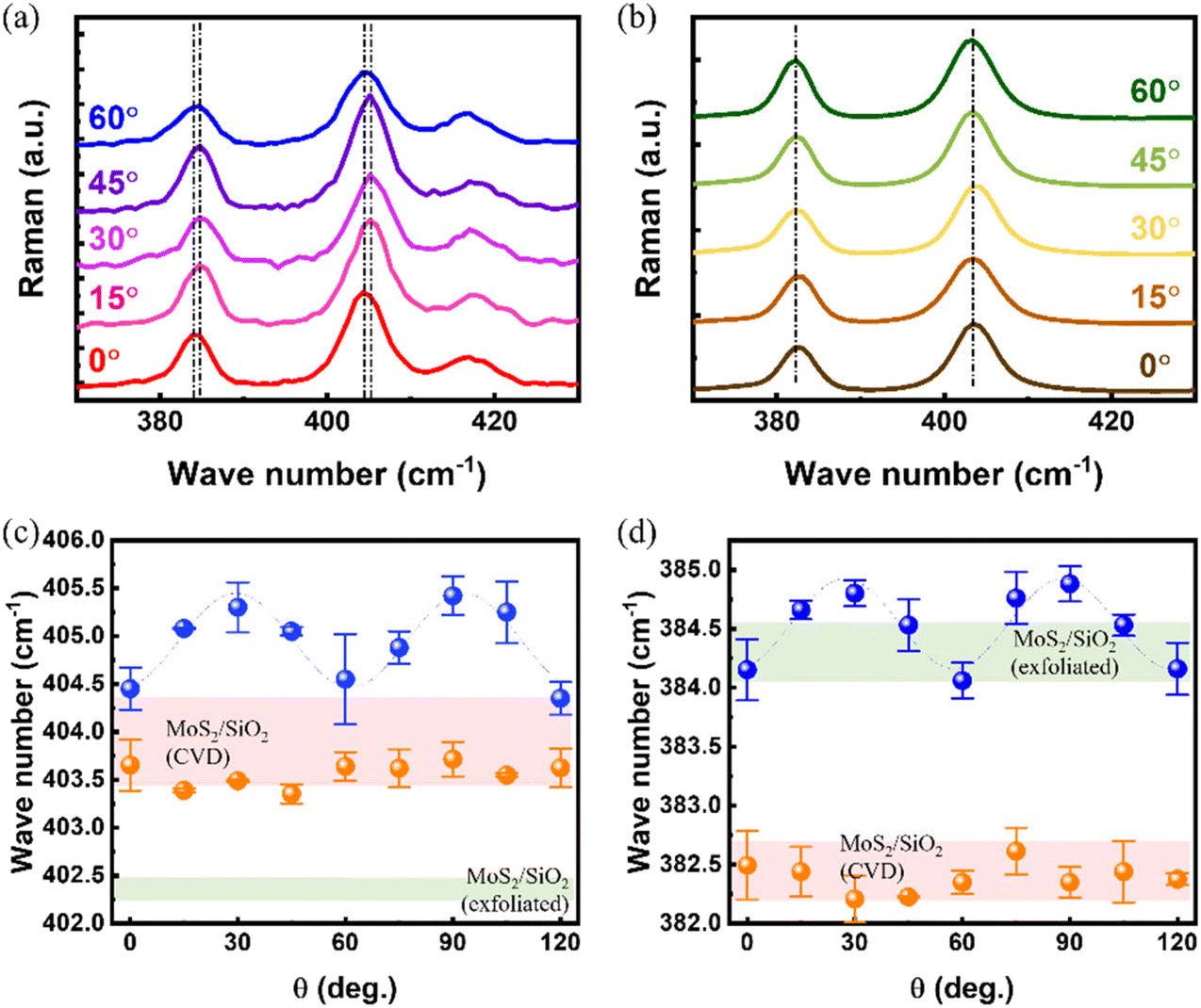 | ||
| Fig. 3 θ-Dependent Raman spectra acquired from the (a) MoS2/Al2O3 and (b) MoS2/SiO2 stacks. The wave number difference (Δk) between the E12g and A1g states is approximately 20 cm−1, suggesting the characteristics of MoS2 monolayers. Plots of the (c) A1g and (d) E12g states acquired from the MoS2/Al2O3 and MoS2/SiO2 stacks with the θ-dependence. The Raman spectra were acquired using a Raman spectroscopy system with an argon CW laser source of 533 nm of 75 mW at room temperature under the atmosphere. The green and pink shadows in (c) and (d) highlight the E12g and A1g states acquired from the MoS2/SiO2 stack fabricated using CVD and exfoliation methods for identifying the tensile strained/n-doped and strain-free/electrically neutral conditions of MoS2 monolayers, respectively ref. 26. Error bars were defined by the difference between the peak positions of the E12g and A1g states and the peaks fitted via the Gaussian–Lorentzian function. | ||
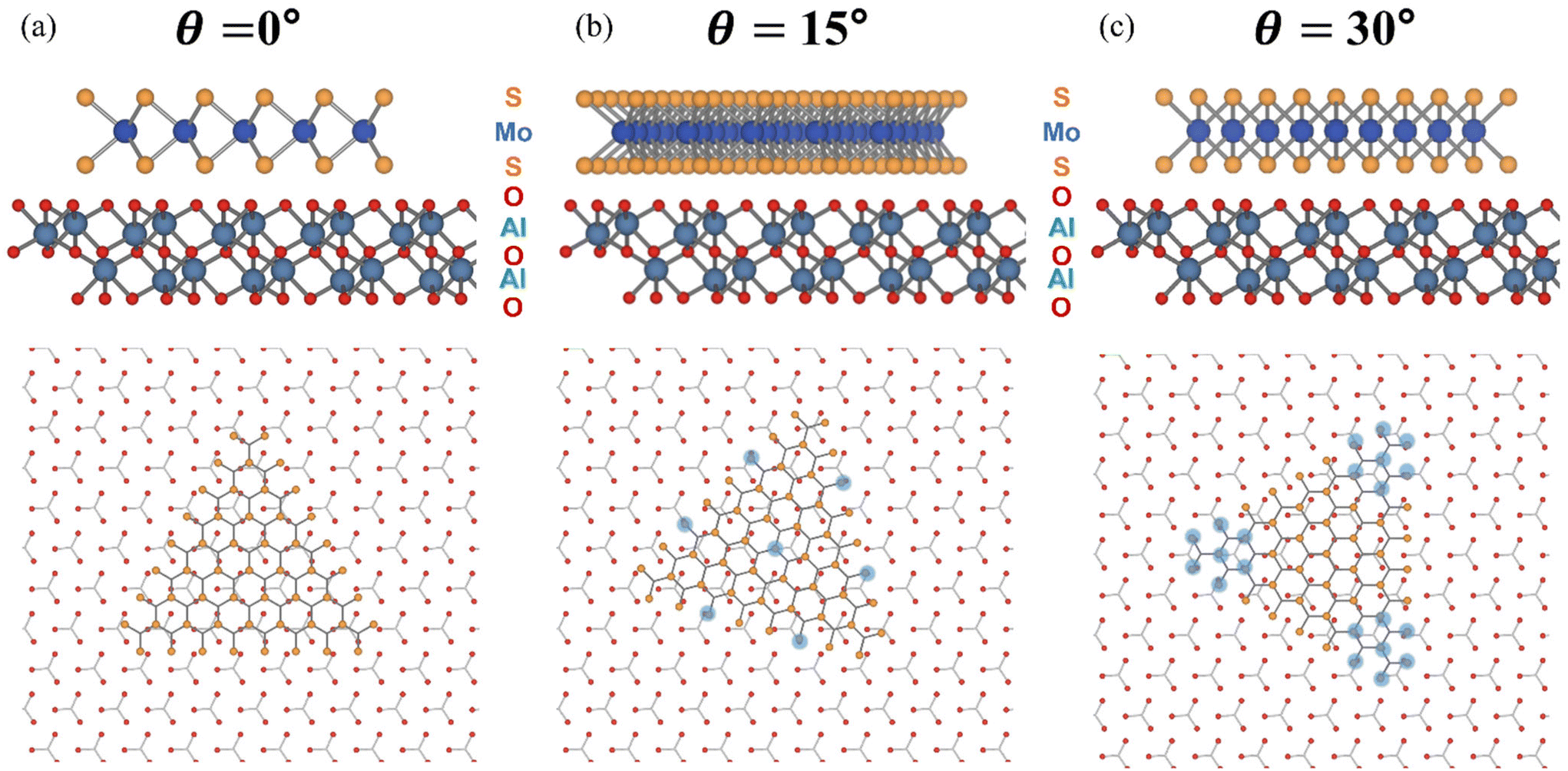 | ||
| Fig. 4 Simulated MoS2/Al2O3 stack images for (a) θ = 0, (b) θ = 15, and (c) θ = 30 degrees via side-viewing (top panel) and top-viewing (bottom panel). The orange, blue, red, and green atoms represent S, Mo, O, and Al, respectively. The blue spots in the top-view images of each bottom panel highlight the site where the S and O atoms are superimposed, namely, the S atoms populate directly or partially on top of the O atoms. Note: for the top-view image, only the S and O atoms are left to demonstrate the superimposition issue because the S and O atoms are in the first contact layer. | ||
4. Discussion
This study demonstrates a strong 6-fold correlation between the exciton state and the stacking geometry of MoS2 monolayers on a sapphire substrate. Based on the previous literature, the variation in exciton energy in the MoS2/Al2O2 stack may arise from three possibilities: (1) dielectric screening effects,32,33 (2) tensile strain-induced band structure modification,34,35 and (3) the doping effect.26 The former two can be revealed through changes in the E12g state, and the latter one can be revealed through the A1g state. Yuxuan Lin et al. reported that the dielectric screening effect can be tuned by varying the dielectric environment of the MoS2 monolayer. Their study observed a blueshift of ∼20 meV on PL upon increasing the solvent dielectric constant from 2 to ∼33.33 In our case, the energy shift in the exciton state is approximately 30 meV from θ = 0° to θ = 30°. Therefore, we can reasonably exclude the dielectric screening and doping effect as a striking factor in driving the exciton change, since the stacking geometry should only give rise to limited changes in the dielectric environment and the extra doping. Another scenario involves the issues of strain and stress. Zhiwei Li et al. reported that a tensile stress can be applied to the MoS2 monolayer using a flexible membrane, PVA.35 In this scenario, an energy redshift of ∼30 meV at the exciton state on PL together with an E12g shift of ∼1 cm−1 was observed when applying a tensile strain of ∼1.5%.35 These results are very close to our observations in the θ-dependent PL and Raman spectra of the MoS2/Al2O2 stack. It could be noticed that the exciton state of the strain-free MoS2 in the study is approximately at 1.88 eV,35 coinciding with the model as proposed in Fig. 4c for the case of θ = 30°. Besides, it has been reported that bandgap reduction36 and the S vacancy may be attributed to the tensile strain,37 which electronically serves as the n-doping source in the θ = 0°/60° stack, thus leading to the observation of A1g softening. Although the thermally induced strain might also be considerable for observing the transition of the exciton state of the MoS2 monolayer,38 that should be still limited in this study because all the MoS2 monolayers investigated were distributed on the same sapphire substrate with the nearly identical morphology. It should be noted that the effects of electron cloud redistribution due to changes in the van der Waals gap distance, which accompany variations in θ, cannot be entirely excluded. However, we still adopt a conservative stance on this matter due to the lack of direct evidence demonstrating the occurrence of electron cloud redistribution. Therefore, we believe, at this stage, that the strain/stress issue arising from the atomic stacking at the MoS2/Al2O3 interface should play a major role in mediating the exciton state of the MoS2 monolayer, which can be tailored through the Moiré correlation with the sapphire substrate.5. Conclusions
In summary, this study explores the intrinsic tuning of the exciton state in MoS2 monolayers grown on a c-cut single-crystalline sapphire substrate by manipulating different Moiré correlations, which has been overlooked in the past but may open another research branch in twistronics. By employing a chemical vapor deposition technique, the MoS2 monolayers were observed to exhibit random orientation on the sapphire substrate, resulting in a wide distribution of stacking morphology. This variability provided an adaptable platform to investigate how specific Moiré correlations influence the exciton state. Interestingly, the exciton state reflected in the photoluminescence spectra appeared to be sensitive to changes in θ, exhibiting a 6-fold correlation during θ-dependent probing. A blueshift transition in the exciton state was observed as the structural stacking between MoS2 monolayers and the sapphire substrate weakened, achievable by misaligning both [100] and sapphire [100]. The stacking geometry would give rise to various degrees of packing density, hence leading to the variable tensile stress in the MoS2 plane as a result of its lattice mismatch with Al2O3. Based on spectroscopic characterization, the intrinsic tuning of the exciton state seems to be adjustable based on specific Moiré correlations via altering the local contact configuration established in the sapphire/MoS2 heterostructure, providing a versatile platform to explore associated physical properties such as charge-density-wave or band structural engineering.
Author contributions
CWC and FMC co-conceived and conducted the experiments under the supervision of CYY. LCC assisted in MoS2 syntheses under the supervision of SKC and took care of the spectroscopic characterization. FMC aided in measurements of Raman and PL spectra. CWC performed the analyses and drafted the manuscript. CYY revised the manuscript and structured the logic of the study. All authors commented on the manuscript to improve the quality and readability.Data availability
The data that support the findings of this study are available from the corresponding author upon reasonable request.Conflicts of interest
No potential conflict of interest was reported by the authors.Acknowledgements
This work is supported by the National Science and Technology Council of Taiwan (NSTC) under grant NSTC-112-2112-M-A49-026/113-2124-M-A49-004/113-2112-M-A49-012 for CYY and 110-2112-M-035-001-MY3 for SKC, and was also supported by the Higher Education Sprout Project and Center for Emergent Functional Matter Science of National Yang Ming Chiao Tung University from The Featured Areas Research Center Program within the framework of the Higher Education Sprout Project by the Ministry of Education (MOE) in Taiwan.References
- A. Taffelli, S. Dirè, A. Quaranta and L. Pancheri, Sensors, 2021, 21, 2758 CrossRef CAS PubMed.
- G. Zhang, H. Liu, J. Qu and J. Li, Energy Environ. Sci., 2016, 9, 1190 RSC.
- A. Zafar, H. Nan, Z. Zafar, Z. Wu, J. Jiang, Y. You and Z. Ni, Nano Res., 2017, 10, 1608 CrossRef CAS.
- L. Huang, A. Krasnok, A. Alú, Y. Yu, D. Neshev and A. E. Miroshnichenko, Rep. Prog. Phys., 2022, 85, 046401 CrossRef CAS PubMed.
- L. Xu, L. Zhao, Y. Wang, M. Zou, Q. Zhang and A. Cao, Nano Res., 2019, 12, 1619 CrossRef CAS.
- A. Splendiani, L. Sun, Y. Zhang, T. Li, J. Kim, C.-Y. Chim, G. Galli and F. Wang, Nano Lett., 2010, 10, 1271 CrossRef CAS PubMed.
- X. Zhang, Z. Lai, C. Tan and H. Zhang, Angew. Chem., Int. Ed., 2016, 55, 8816 CrossRef CAS PubMed.
- A. Özden, F. Ay, C. Sevik and N. K. Perkgöz, Jpn. J. Appl. Phys., 2017, 56, 06GG05 CrossRef.
- S. Aftab and H. H. Hegazy, Small, 2023, 19, 2205778 CrossRef CAS PubMed.
- Y. Liu, Y. Gao, S. Zhang, J. He, J. Yu and Z. Liu, Nano Res., 2019, 12, 2695 CrossRef CAS.
- G. Kioseoglou, A. T. Hanbicki, M. Currie, A. L. Friedman, D. Gunlycke and B. T. Jonker, Appl. Phys. Lett., 2012, 101, 221907 CrossRef.
- A. Singh, Y. Li, B. Fodor, L. Makai, J. Zhou, H. Xu, A. Akey, J. Li and R. Jaramillo, Appl. Phys. Lett., 2019, 115, 161902 CrossRef.
- T. Mueller and E. Malic, npj 2D Mater. Appl., 2018, 2, 29 CrossRef.
- K. Liu, L. Zhang, T. Cao, C. Jin, D. Qiu, Q. Zhou, A. Zettl, P. Yang, S. G. Louie and F. Wang, Nat. Commun., 2014, 5, 4966 CrossRef CAS PubMed.
- S. Huang, X. Ling, L. Liang, J. Kong, H. Terrones, V. Meunier and M. S. Dresselhaus, Nano Lett., 2014, 14, 5500 CrossRef CAS PubMed.
- S. Zheng, L. Sun, X. Zhou, F. Liu, Z. Liu, Z. Shen and H. J. Fan, Adv. Opt. Mater., 2015, 3, 1600 CrossRef CAS.
- L. Kang, D. Tian, L. Meng, M. Du, W. Yan, Z. Meng and X.-a. Li, Surf. Sci., 2022, 720, 122046 CrossRef CAS.
- J. Lu, M. Zheng, J. Liu, Y. Zhang, X. Zhang and W. Cai, Nanomaterials, 2023, 13, 3056 CrossRef CAS PubMed.
- A. Jain, S. P. Ong, G. Hautier, W. Chen, W. D. Richards, S. Dacek, S. Cholia, D. Gunter, D. Skinner, G. Ceder and K. A. Persson, APL Mater., 2013, 1, 011002 CrossRef.
- J. Lewis, D. Schwarzenbach and H. D. Flack, Acta Crystallogr., Sect. A, 1982, 38, 733 CrossRef.
- D. Dumcenco, D. Ovchinnikov, K. Marinov, P. Lazić, M. Gibertini, N. Marzari, O. L. Sanchez, Y.-C. Kung, D. Krasnozhon, M.-W. Chen, S. Bertolazzi, P. Gillet, A. Fontcuberta i Morral, A. Radenovic and A. Kis, ACS Nano, 2015, 9, 4611 CrossRef CAS PubMed.
- L. Li, Q. Wang, F. Wu, Q. Xu, J. Tian, Z. Huang, Q. Wang, X. Zhao, Q. Zhang, Q. Fan, X. Li, Y. Peng, Y. Zhang, K. Ji, A. Zhi, H. Sun, M. Zhu, J. Zhu, N. Lu, Y. Lu, S. Wang, X. Bai, Y. Xu, W. Yang and G. Zhang, Nat. Commun., 2024, 15, 1825 CrossRef CAS PubMed.
- A. Rai, A. Valsaraj, H. C. P. Movva, A. Roy, R. Ghosh, S. Sonde, S. Kang, J. Chang, T. Trivedi, R. Dey, S. Guchhait, S. Larentis, L. F. Register, E. Tutuc and S. K. Banerjee, Nano Lett., 2015, 15, 4329 CrossRef CAS PubMed.
- N. Scheuschner1, O. Ochedowski, A.-M. Kaulitz, R. Gillen, M. Schleberger and J. Maultzsch, Phys. Rev. B:Condens. Matter Mater. Phys., 2014, 89, 125406 CrossRef.
- T. Han, H. Liu, S. Wang, S. Chen, W. Li, X. Yang, M. Cai and K. Yang, Nanomaterials, 2019, 9, 740 CrossRef CAS PubMed.
- A. Michail, N. Delikoukos, J. Parthenios, C. Galiotis and K. Papagelis, Appl. Phys. Lett., 2016, 108, 173102 CrossRef.
- N. Scheuschner, O. Ochedowski, A.-M. Kaulitz, R. Gillen, M. Schleberger and J. Maultzsch, Phys. Rev. B:Condens. Matter Mater. Phys., 2014, 89, 125406 CrossRef.
- Y. Liu, T. Shen, S. Linghu, R. Zhua and F. Gu, Nanoscale Adv., 2022, 4, 2484 RSC.
- F. Tumino, P. D'Agosta, V. Russo, A. L. Bassi and C. S. Casari, Crystals, 2023, 13, 1271 CrossRef CAS.
- C.-Y. Yang, L. Pan, A. J. Grutter, H. Wang, X. Che, Q. L. He, Y. Wu, D. A. Gilbert, P. Shafer, E. Arenholz, H. Wu, G. Yin, P. Deng, J. A. Borchers, W. Ratcliff II and K. L. Wang, Sci. Adv., 2020, 6, eaaz8463 CrossRef CAS PubMed.
- J. Zhang, J. Wang, P. Chen, Y. Sun, S. Wu, Z. Jia, X. Lu, H. Yu, W. Chen, J. Zhu, G. Xie, R. Yang, D. Shi, X. Xu, J. Xiang, K. Liu and G. Zhang, Adv. Mater., 2016, 28, 1950 CrossRef CAS PubMed.
- L. Liang and V. Meunier, Nanoscale, 2014, 6, 5394 RSC.
- Y. Lin, X. Ling, L. Yu, S. Huang, A. L. Hsu, Y.-H. Lee, J. Kong, M. S. Dresselhaus and T. Palacios, Nano Lett., 2014, 14, 5569 CrossRef CAS PubMed.
- T. Peña, S. A. Chowdhury, A. Azizimanesh, A. Sewaket, H. Askari and S. M. Wu, 2D Mater., 2021, 8, 045001 CrossRef.
- Z. Li, Y. Lv, L. Ren, J. Li, L. Kong, Y. Zeng, Q. Tao, R. Wu, H. Ma, B. Zhao, D. Wang, W. Dang, K. Chen, L. Liao, X. Duan, X. Duan and Y. Liu, Nat. Commun., 2020, 11, 1151 CrossRef CAS PubMed.
- A. Castellanos-Gomez, R. Roldán, E. Cappelluti, M. Buscema, F. Guinea, H. S. J. van der Zant and G. A. Steele, Nano Lett., 2013, 13, 3626 CrossRef PubMed.
- C.-Y. Yang, K.-C. Chiu, S.-J. Chang, X.-Q. Zhang, J.-Y. Liang, C.-S. Chung, H. Pan, J.-M. Wu, Y.-C. Tseng and Y.-H. Lee, Nanoscale, 2016, 8, 5627 RSC.
- L. Seravalli, F. Esposito, M. Bosi, L. Aversa, G. Trevisi, R. Verucchi, L. Lazzarini, F. Rossi and F. Fabbri, Nanoscale, 2023, 15, 14669 RSC.
Footnote |
| † Electronic supplementary information (ESI) available. See DOI: https://doi.org/10.1039/d4nr03935a |
| This journal is © The Royal Society of Chemistry 2025 |