
 Open Access Article
 This Open Access Article is licensed under a
 Creative Commons Attribution 3.0 Unported Licence
Hf0.5Zr0.5O2/HfO2/Hf0.5Zr0.5O2 laminated thin films and CF4 plasma passivation for improved memory and synaptic characteristics of ferroelectric field-effect transistors
Kyungsoo
Park
a,
Chulwon
Chung
b,
Boncheol
Ku
a,
Seunghyeon
Yun
a,
Junhyeok
Park
a and
Changhwan
Choi
 *a
*a
aDivision of Materials Science & Engineering, Hanyang University, Seoul, Korea
bDepartment of Energy Engineering, Hanyang University, Seoul, Korea. E-mail: cchoi@hanyang.ac.kr
First published on 31st January 2025
Abstract
In this study, we demonstrate significant advancements in hafnium oxide-based ferroelectric field-effect transistors (FeFET) by integrating two engineering methods: laminated ferroelectric (FE) thin films and CF4-based plasma treatment. Individually, these techniques exhibit specific trade-offs; however, their combined application effectively mitigates these drawbacks, maximizing their synergistic benefits. Compared to the pristine FeFET, our results demonstrate an improvement in endurance by more than one order of magnitude, while maintaining the same memory window (MW) at 1.2 V, through the application of the proposed engineering. Furthermore, the combined approach significantly enhances the synaptic properties of FeFETs, making them more suitable for analog synapse applications in neuromorphic computing. Specifically, the Gmax/Gmin ratio increased from 4 to 7, the asymmetry value decreased from 4.68 to 3.44, and the number of states rose from 75 to 100. Lastly, through MNIST dataset-based accuracy simulation, the proposed device achieved an inference accuracy of 80%, representing a 10% improvement over the pristine device. These findings suggest that the simultaneous utilization of FE lamination and plasma treatment can be a knob for developing high-performance FeFET-based analog synapses, advancing their potential in memory and neuromorphic computing technologies.
1. Introduction
With the advancement of social networking services (SNS), cloud computing, the Internet of Things (IoT), robotics, and artificial intelligence (AI), the volume of data generated has increased exponentially. These data are mostly unstructured, encompassing formats such as audio, video, and text. However, the current widely used computing architecture, the von Neumann architecture, is inefficient for handling substantial amounts of unstructured data. This inefficiency arises from the need for extensive hardware and interconnections for computing, leading to increased energy consumption and signal delays due to bus bottlenecks, which result from the separation of the processor and memory in this architecture.1–3In contrast, the human brain is an exemplary computing system, capable of superior performance at a mere 20 W power consumption. Inspired by the neural system of the human brain, neuromorphic computing architectures have been developed. These architectures employ parallel processing structures that integrate memory and information processing, enabling ultra-low power and high-speed artificial intelligence operations.4–6 However, to leverage the full potential of neuromorphic architectures, novel hardware structures tailored to these architectures are required.
A critical component of these new hardware structures is the synaptic device, which must meet low power consumption, high-speed operation, and stable synaptic behavior.7–10 Among various types of emerging non-volatile memory (eNVM) devices, hafnium-based FeFETs not only meet the aforementioned requirements but also offer excellent scalability and compatibility with CMOS technology, making them leading candidates for synaptic devices.11–13
Since the introduction of FeFETs, various methods have been explored to enhance their characteristics, including FE quenching,14,15 interfacial layering (IL),16 dopants,3 and metal engineering.17 Among these, FE lamination has been implemented, offering several benefits such as reduced leakage current in the gate stack, improved multi-level cell (MLC) storage, decreased variation, and more linear polarization.18–20 However, this engineering approach has the drawback of reducing remanent polarization (Pr). Another method is fluorine plasma treatment, which enhances the orthorhombic phase (o-phase) fraction and increases the coercive voltage (Vc) or coercive electric field (Ec) in the FE layer of FeFETs. However, a drawback is that gate leakage rises with an increase in oxygen vacancies (Vo), and the regrowth of the interfacial layer (IL) leads to undesirable endurance degradation.21,22
Research on the combined use of these two methods, specifically fluorine plasma treatment on laminated FeFETs, has been limited. In this work, the impact of fluorine plasma on the laminated structure of FeFETs is investigated. Through plasma treatment, the MW of pristine FeFETs increased, and the introduction of the laminated interlayer suppressed undesirable endurance degradation. The synaptic characteristics of FeFETs were also examined. We evaluated these synaptic characteristics of FeFETs with both FE lamination and plasma treatment methods and, furthermore, assessed inference accuracy using simulations based on the extracted synaptic properties.
Our study highlights the potential of combining FE lamination and fluorine plasma treatment to enhance FeFET-based synaptic devices, paving the way for more efficient and high-performance neuromorphic computing systems.
2. Experimental: fabrication and characterization methods
Fig. 1(a) illustrates the schematic of CF4 plasma treatment on a laminated FeFET, while Fig. 1(b) shows the process flow for fabricating metal–ferroelectric–metal (MFM) capacitors and FeFETs using FE lamination and plasma treatment. The FeFETs were fabricated on a p-type Si substrate with a 300 nm-thick SiO2 layer. Initially, photolithography was used to pattern the source/drain (S/D) regions, and SiO2 was etched using a buffered oxide etcher (BOE). Afterward, phosphorus (P+) ion implantation was performed to form n-type S/D regions on the p-Si substrate. Using a medium ion implanter, P+ ions were implanted with a dose of 1 × 10¹⁵, an energy of 40 keV, and an incident angle of 7°. Rapid thermal annealing (RTA) was performed at 950 °C for 10 seconds to activate the implanted ions. Subsequently, photolithography was used again to pattern the channel opening, which was then etched using BOE. | ||
| Fig. 1 (a) Schematic illustrations of the CF4 plasma-treatment process on a laminated FeFET and (b) fabrication flow diagrams of the MFM capacitor and the FeFET with lamination and plasma treatment. | ||
To form the IL of the metal–ferroelectric–insulator–semiconductor (MFIS) gate stack, the substrate was immersed in an ammonia–peroxide mixture (APM) solution (NH4OH![[thin space (1/6-em)]](https://www.rsc.org/images/entities/char_2009.gif) :H2O2:H2O = 1:1:5) at 85 °C for 5 minutes to grow a clean SiO2 layer. Next, a 10 nm-thick Hf0.5Zr0.5O2 (HZO) layer and laminated FE layers (HZO:HfO2:HZO = 5 nm/1 nm/5 nm) were deposited using thermal atomic layer deposition (ALD) at 280 °C. Depending on the splits, CF4 plasma treatment was applied to the FE film. The process pressure and flow rate of CF4 gas were set to 400 mTorr and 100 sccm, respectively, with an RF power of 30 W. The gate metal and S/D contact metals were then formed by sputtering a 35 nm-thick W layer. Finally, post-metal annealing (PMA) was conducted by rapid thermal annealing (RTA) at 600 °C for 30 seconds under ambient N2 to activate the dopants and form the o-phase in the FE layer.
:H2O2:H2O = 1:1:5) at 85 °C for 5 minutes to grow a clean SiO2 layer. Next, a 10 nm-thick Hf0.5Zr0.5O2 (HZO) layer and laminated FE layers (HZO:HfO2:HZO = 5 nm/1 nm/5 nm) were deposited using thermal atomic layer deposition (ALD) at 280 °C. Depending on the splits, CF4 plasma treatment was applied to the FE film. The process pressure and flow rate of CF4 gas were set to 400 mTorr and 100 sccm, respectively, with an RF power of 30 W. The gate metal and S/D contact metals were then formed by sputtering a 35 nm-thick W layer. Finally, post-metal annealing (PMA) was conducted by rapid thermal annealing (RTA) at 600 °C for 30 seconds under ambient N2 to activate the dopants and form the o-phase in the FE layer.
Cross-sectional high-resolution transmission electron microscopy (HR-TEM) and energy dispersive X-ray spectroscopy (EDS) analyses were performed with the FeFET gate stack with and without FE lamination. In addition, X-ray photoelectron spectroscopy (XPS) and grazing incident X-ray diffractometry (GI-XRD) analyses were performed for chemical determination of the four different FE films. The XPS analysis was conducted with an Al Kα X-ray source. The scan was conducted from 1350 eV to 0 eV and the energy step size of the XPS survey spectra was 1 eV.
Electrical properties of MFMs and FeFETs with four different gate stacks were measured with Keithley 4200A-SCS and Keysight B1500A devices, which are semiconductor characteristic measurement instruments. Four different types of gate stack are as follows: untreated HZO (pristine), plasma-treated HZO (pristine plasma), untreated laminated HZO (LAM), and plasma-treated laminated HZO (LAM plasma). Furthermore, all electrical measurements were conducted at room temperature under an ambient atmosphere. The polarization–voltage (P–V) graphs of the MFM structures were recorded using triangular pulses with both rise and fall times of 10 μs. Device-to-device variation in the MFM capacitors was determined by measuring identically sized capacitors fabricated simultaneously.
For all FeFETs, the MW was extracted from the transfer curves obtained by dual sweeping the gate voltage with a constant drain voltage. The low and high threshold voltages (LVT and HVT) were determined using the constant current method (10−7 W L−1 [A]), and the MW was calculated as the difference between these voltages. To evaluate the endurance characteristics of the FeFETs, a positive-up–negative-down (PUND) pulse sequence with a voltage amplitude of 4 V and a pulse width of 10 μs was used.
The long-term potentiation (LTP) and long-term depression (LTD) characteristics of the FeFETs were extracted using an incremental pulse scheme. For inference accuracy simulations, a two-layer multi-layer perceptron (MLP) neural network (NN) and the Modified National Institute of Standards and Technology Database (MNIST) handwritten digits dataset were employed.
3. Results and discussion
3.1. Effects of lamination and plasma treatment on the ferroelectric property
Fig. 2 presents HR-TEM images and EDS analysis of pristine and laminated gate stack structures. Fig. 2(a and b) demonstrates the well-crystallized structure of both the pristine and LAM HZO layers. Moreover, the fast Fourier transformation (FFT) pattern obtained from a selected region and the reverse FFT image created after filtering reveal an interplanar distance of 2.94 Å, confirming the formation of the ferroelectric o-phase in both the pristine and LAM structures. In Fig. 2(c and d), pristine HZO shows a similar ratio of Hf and Zr contents throughout the entire film, whereas in the LAM HZO, the Hf fraction is significantly higher than Zr in the middle of the film. This indicates that the LAM structure, with the HfO2 dielectric (DE) layer inserted in the middle, has been properly formed. The thicknesses of the single HZO FE layer and the LAM FE layer were intentionally set to 10 nm and 11 nm, respectively, to ensure that the HZO FE layer thickness remains consistent at 10 nm across both structures. This intentional design was aimed at enabling a clear and reliable evaluation of the impact of the inserted DE layer on the FE properties. If the total thickness was constrained to 10 nm by modifying the thickness of the HZO FE layer (e.g. configuring HZO/HfO2/HZO as 4.5 nm/1 nm/4.5 nm), the overall FE layer thickness would differ between the pristine and LAM structures. In such a case, it would become challenging to determine whether the observed changes in FE properties were due to the insertion of the DE layer or merely the reduction in the FE layer thickness. While it is acknowledged that variations in total thickness may also influence FE characteristics, fixing the HZO FE layer thickness at 10 nm is deemed a more practical and controlled approach to isolate and evaluate the effect of the inserted DE layer. This strategy minimizes potential confounding factors and ensures a more reliable interpretation of the experimental results. Additionally, the reason we chose HfO2 as the DE layer, among various options, is its relatively high dielectric constant (k) compared to that of other materials. While many studies have employed Al2O3 as the DE layer,19,20,23 HfO2 has a significantly higher k-value (kAl2O3 ∼ 9, kHfO2 ∼ 25). Using a DE material with a higher k-value induces a larger voltage drop across the HZO FE layer under the same applied voltage. This results in an increased Pr and a reduced Ec, making the structure suitable for low-power operation and facilitating the development of optimized thin films.24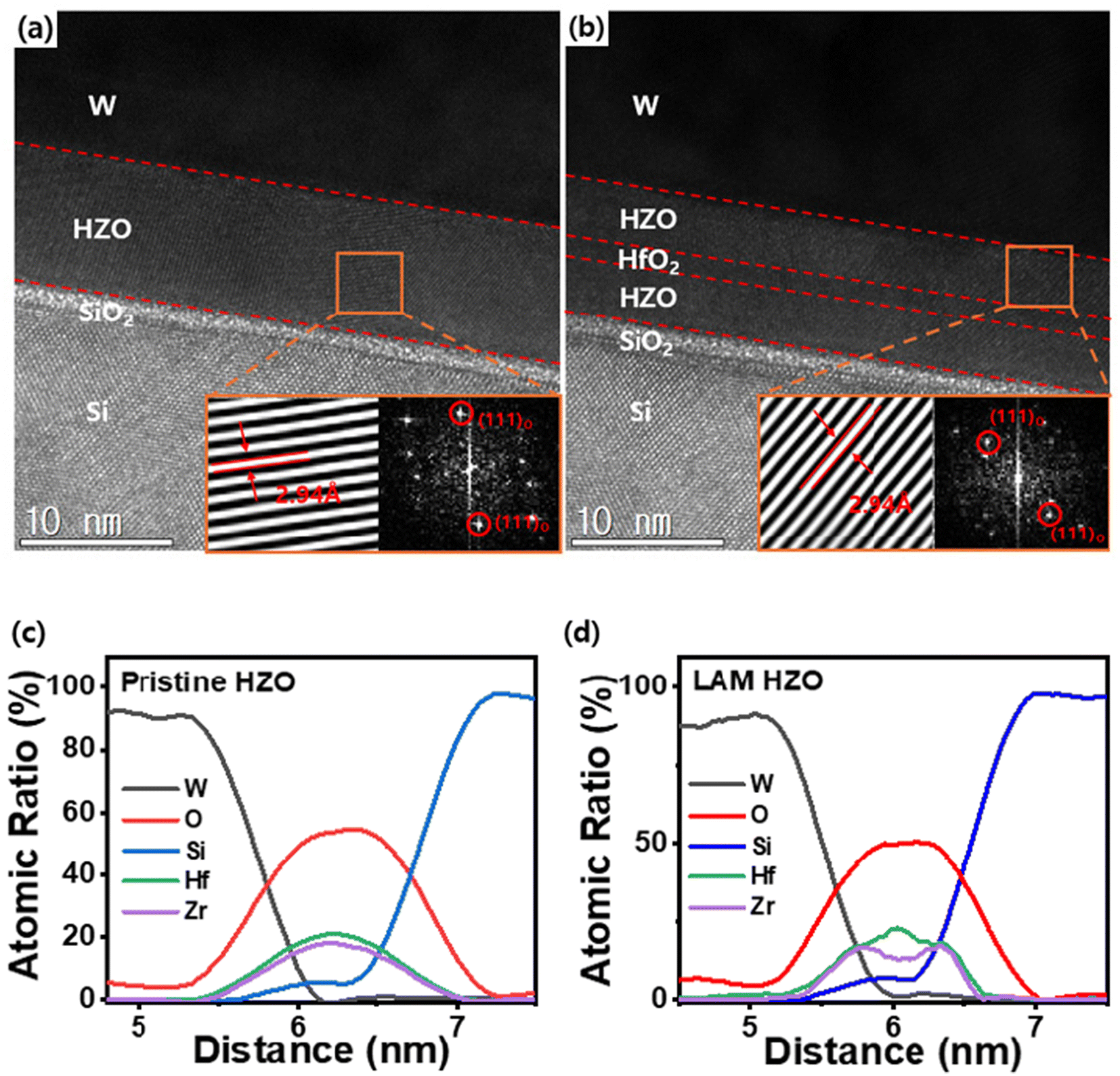 | ||
| Fig. 2 Cross-sectional HR-TEM images and EDS analysis graphs of (a and c) pristine HZO and (b and d) LAM HZO. For better visibility, the reverse FFT images were obtained from the FFT patterns. | ||
Fig. 3 illustrates P–V characteristics of the MFM structures (with a gate electrode size of 100 μm × 100 μm) measured using triangular pulses at a frequency of 25 kHz. These properties highlight the effects of the laminated structure and plasma treatment on the FE layer. It can be observed that plasma treatment increases both the Pr and Ec values compared to those of untreated films, regardless of the pristine or laminated structure. Additionally, applying the laminated structure results in a decrease in Pr compared to pristine. The difference in |−Ec| and |+Ec| observed across all samples can be attributed to the positive-direction imprint effect in the P–V loops. More specifically, this behavior is linked to a unique characteristic of hafnia-based FE known as fluid imprint.25 The imprint effect in the P–V loop refers to the phenomenon where an electrical bias causes the P–V curve to shift along the voltage axis. Unlike a conventional imprint, which develops gradually over time in polarized capacitors, the fluid imprint is highly dependent on measurement conditions and switching history, making it more dynamic and easier to alter. The positive-direction shift in the P–V curves for all samples is caused by the structure of the triangular pulses used during measurement. Specifically, the triangular pulse starts with a positive amplitude before transitioning to a negative amplitude. To properly measure the P–V curve, a setup pulse with an amplitude opposite to the initial triangular pulse amplitude is typically used to pre-align the FE dipoles. As mentioned, in our measurements, the triangular pulse rises to a positive amplitude and falls to a negative amplitude, requiring the setup pulse to have a negative amplitude. Using a negative amplitude setup pulse leads to electron trapping at the interface between the top electrode and the FE layer (conversely, a positive setup pulse would trap electrons at the interface between the bottom electrode and the FE layer). The trapped electrons on the top electrode generate an internal electric field within the film, which opposes the external electric field applied during the positive triangular pulse measurement. Consequently, the external field must compensate for the internal field to align the dipoles in the positive direction, resulting in an increase in +Ec. Conversely, the internal field assists dipole alignment in the negative direction, leading to a decrease in −Ec, thereby causing the observed imprint effect. This imprint effect is more pronounced in the LAM structure compared to the pristine structure due to the thicker overall film thickness in the LAM samples. As the film thickness increases, the overall capacitance of the film decreases, leading to a greater voltage drop across the film. This increased voltage drop promotes charge trapping, thereby amplifying the imprint effect. Furthermore, the ratios of (|+Ec|/|−Ec|) for the pristine, pristine plasma, LAM, and LAM plasma samples are 28%, 24%, 33%, and 30%, respectively. These ratios indicate that plasma-treated samples exhibit a reduced imprint effect across all structures. This reduction can be attributed to the surface defect passivation effect of plasma treatment. (The surface defect passivation mechanism of plasma treatment will be discussed further in a subsequent section.)
 | ||
| Fig. 3 Effects of plasma treatment on P–V characteristics of (a) pristine and (b) LAM-structured MFM capacitors. | ||
To understand the mechanism behind the increase in Pr and Ec due to plasma treatment, XPS and GI-XRD analyses were conducted. Fig. 4(a) shows the ratios of Hf–O bonds and Hf–F bonds for pristine, pristine plasma, LAM, and the LAM plasma structure. CF4 plasma treatment significantly increases the Hf–F bond ratio compared to untreated samples. Furthermore, as shown in Fig. 4(b), the sub-oxides ratio, which is consistent with the ratio of Vo, was higher in the plasma-treated films. This suggests that CF4 plasma treatment replaces Hf–O bonds with Hf–F bonds, increasing Vo. GI-XRD analysis revealed an increase in the o(111)/t(011) peak with plasma treatment (Fig. 4(c)). Deconvolution of this peak into the o-phase and t-phase indicated a significant increase in the o-phase fraction due to plasma treatment (Fig. 4(d)). Summarizing the XPS and GI-XRD analyses, plasma treatment increases Vo in the film, which induces tensile stress in the film during crystallization annealing, enhancing the o-phase fraction.26,27 Furthermore, appropriately pinning the FE domain, Vo also increases Vc of the FE layer. While plasma treatment has the advantage of increasing Pr and Ec, it also creates Vo that acts as defects within the film, deteriorating endurance properties. The decrease in Pr with the application of a laminated structure is due to the depolarization field caused by the DE layer inserted between the upper and lower FE layers.28 However, the inserted DE layer also improves the endurance of the film by reducing gate leakage current.19,23 Furthermore, it increases the number of decomposed FE domains, reducing polarization variation and enabling more linear polarization updates.18
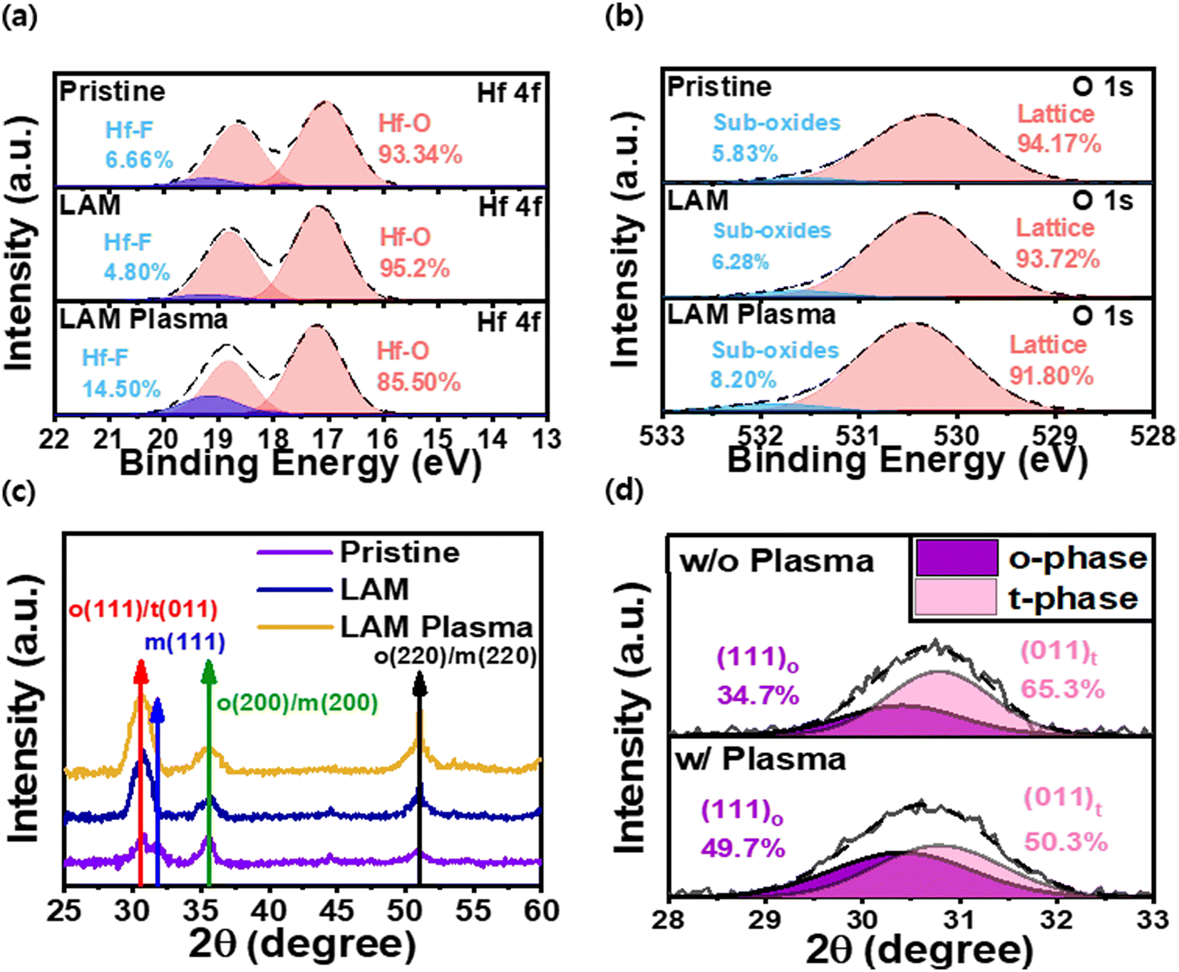 | ||
| Fig. 4 XPS and GI-XRD analysis of pristine, pristine plasma and LAM plasma HZO FE layers. (a) Ratio of Hf–F and Hf–O bonding through deconvolution of the binding energy peaks in the XPS spectra of Hf 4f. (b) Ratio of sub-oxide (Vo) to lattice oxide in the thin film through deconvolution of the binding energy peaks in the XPS spectra of O 1s. (c) Distribution of crystalline phases in the thin film determined through GI-XRD, and (d) fraction of o-phase and t-phase, depending on plasma treatment through the deconvolution of the o(111)/t(001) peaks. | ||
Fig. 5 presents the device-to-device variation and leakage current characteristics of four different MFM capacitors. In Fig. 5(a), it can be observed that applying the laminated structure reduces the device-to-device variation, and this reduced variation is maintained even after plasma treatment. Fig. 5(b) shows that the plasma treatment increases the Vo in the thin HZO film, leading to an increase in leakage current. However, applying a laminated structure decreases the leakage current. This indicates that FE lamination can reduce device-to-device variation and leakage current, thereby enhancing the reliability of the device.
 | ||
| Fig. 5 (a) 2Pr device-to-device variation of MFM capacitors and (b) leakage current density of different FE films: pristine HZO, plasma-treated pristine HZO, laminated HZO, and plasma-treated laminated HZO. | ||
3.2. Memory and endurance characteristics of the FeFET with two engineering methods
Fig. 6 shows the transfer curves and MW of the four different splits of FeFETs. The channel width and length of the fabricated FeFETs are 40 μm and 20 μm, respectively. The gate voltage (VG) sweep range is set from −4 V to 4 V, and the drain voltage (VD) is set at 0.1 V. The pristine FeFET and laminated FeFET subjected to plasma treatment show an increase in MW by 0.3 V and 0.2 V, respectively, compared to the untreated ones. This indicates that plasma treatment increases the Pr and Ec of the FE thin film, thereby enhancing MW, regardless of whether it is a pristine HZO structure or a laminated structure. Furthermore, FeFETs with a laminated structure exhibit a lower MW compared to pristine FeFETs. This is attributed to the depolarization field caused by the DE layer in the laminated structure, which reduces the Pr of the FE thin film. However, the FeFETs with a laminated structure show lower off-current values than pristine FeFETs, indicating that the DE layer inserted in the middle of the laminated structure mitigates the leakage current. It should also be noted that when fluorine plasma treatment is applied to a pristine FeFET structure, the overall transfer curve shifts to the positive direction. This is because the fluorine atoms introduced into the HZO thin film during the plasma treatment carry negative charges. These negatively charged ions cause the threshold voltage (Vt) to shift to the positive direction.29 However, in the case of the LAM FeFET structure, this Vt shift is minimal. This is likely due to the HfO2 DE layer inserted in the middle of the LAM structure, which acts as a diffusion barrier, preventing the diffusion of fluorine ions with negative charges into the thin film. | ||
| Fig. 6 Transfer curve and extracted MW of (a) the pristine structure and pristine plasma FeFET and (b) the LAM structure and LAM plasma FeFET. | ||
Although not shown in the figure, we further evaluated the effects of variations in channel length, width, and drain voltage on the Id − Vg transfer characteristics of FeFET devices, beyond the conditions of 40 μm and 20 μm channel dimensions and a drain voltage of 0.1 V. The results indicated that changes in channel length did not significantly affect the Id − Vg transfer characteristics of the FeFET. This finding can be attributed to the negligible influence of channel length variations on device performance at the micrometer scale. However, we anticipate that if the channel length is scaled down to the nanometer range, the FeFET, due to its structural resemblance to a MOSFET, would exhibit short channel effects. In contrast, variations in channel width had a significant impact on the Id − Vg transfer characteristics. Specifically, an increase in channel width led to improvements in both the MW and the on/off current ratio. The increase in MW is explained by the enhanced overlap between the gate metal and the S/D regions as the channel width expands. This increased overlap strengthens the electric field applied across the HZO layer, facilitating more efficient switching of FE dipoles and consequently widening the MW.30 Moreover, the increase in on/off current with greater channel width can be attributed to a reduction in channel resistance. The electron conduction path from the source to the drain can be modeled as a series connection of the source/drain resistance and channel resistance. Therefore, a decrease in channel resistance reduces the total resistance, enhancing the overall current flow. Finally, we investigated the impact of varying drain voltage on the transfer characteristics. Changes in drain voltage caused a shift in the transfer curve along the z-axis. Notably, when the drain voltage exceeded 0.5 V, both the MW and the on/off current ratio decreased. The reduction in MW is attributed to a decreased voltage difference between the gate and drain, which makes switching of the ferroelectric dipoles more difficult. Additionally, the reduction in the on/off ratio is explained by the saturation of the on-current, constrained by the maximum limit of electron mobility, while the off-current continues to increase.
Fig. 7 shows the PUND pulse scheme used for endurance measurement and the characteristics of the four different FeFETs. In Fig. 7(a), the amplitude and width of the PUND pulses for endurance measurement are set to 4 V and 10 μs, respectively, which fully switches the polarization of the FE layer. As shown in Fig. 7(b), all pristine FeFETs, regardless of plasma treatment, lose their MW after 105 cycles. However, FeFETs with the laminated structure maintained a robust MW even beyond 106 cycles, despite implementing plasma treatment. This improvement is attributed to the reduced gate leakage current due to the laminated structure. The reduction in leakage current observed with the LAM structure can be attributed to the DE layer inserted in the middle, which prevents the formation of grain boundaries within the HZO film.19,23 Grain boundaries are a primary cause of increased leakage current, as they provide continuous pathways for current flow. Consequently, the thin HfO2 DE layer suppresses the formation of grain boundaries, interrupting the leakage current paths.
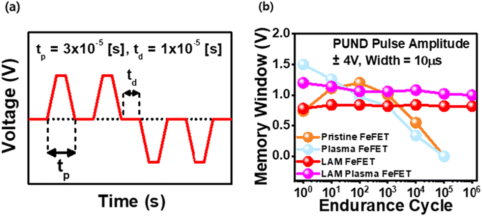 | ||
| Fig. 7 (a) PUND pulse scheme used for endurance measurements and (b) MW characteristics of four different FeFETs. | ||
Additionally, plasma-treated FeFETs, which are pristine plasma and LAM plasma FeFETs, exhibit wakeup-free characteristics. The wake-up effect, commonly observed in an HZO-based FE, arises from locally distributed Vo or surface defects at the HZO–metal interface, which redistribute throughout the film during wake-up cycles.31 In FeFETs treated with fluorine plasma, the wake-up-free behavior can be attributed to the distinct roles of plasma treatment on the surface and in the bulk of FE thin films. As discussed earlier and shown in Fig. 4, in the bulk, fluorine atoms with high electronegativity can break Hf–O and Zr–O bonds, replacing them with Hf–F and Zr–F bonds. This process generates new Vo, contributing to changes in the bulk properties.21 On the surface, however, the effect is different. Fluorine atoms passivate defects such as Vo and dangling bonds. The high electronegativity and reactivity of fluorine enable it to bond with these defects, stabilizing the surface. This phenomenon has been validated in various prior studies.22,32 As a result, fluorine plasma treatment effectively passivates surface defects, preventing their redistribution and significantly reducing the wake-up effect.
3.3. Synaptic characteristics and system-level inference accuracy simulation
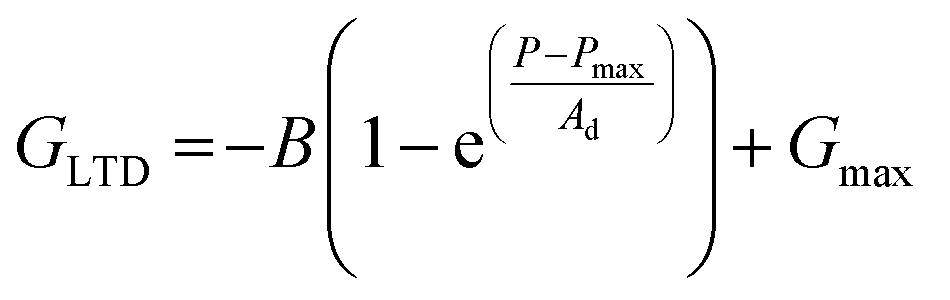
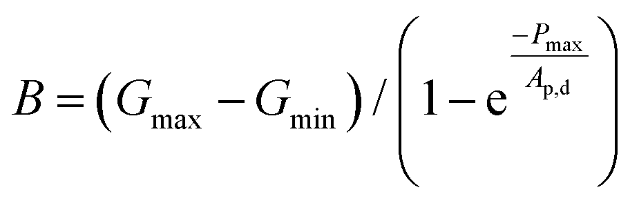
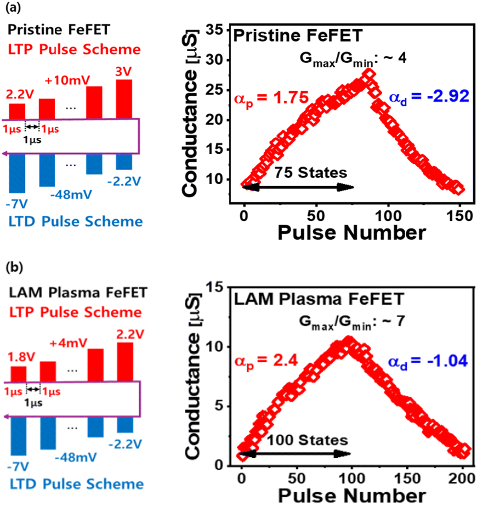
Fig. 8 illustrates the LTP/LTD characteristics of the pristine FeFET and laminated plasma FeFET. LTP and LTD characteristics are essential for synaptic devices to mimic the learning and long-term memory mechanisms of biological neural networks. Through these mechanisms, synaptic devices can achieve high performance in terms of information storage, learning efficiency, neural plasticity, and stability. Fig. 8(a) presents the pulse scheme used to evaluate the LTP/LTD characteristics of the pristine FeFET and LAM plasma FeFET. The pulse scheme is designed to exhibit the optimal LTP/LTD characteristics of each FeFET. The reason for the relatively lower amplitude of the pulse scheme for LTD compared to that for LTP is that electrons have a greater impact than holes in changing the polarization of the ferroelectric layer.33 Nonlinearity, asymmetry value, Gmax/Gmin ratio, and the number of states are key parameters used to evaluate how effectively a synaptic device can mimic LTP/LTD characteristics. The nonlinearity value was extracted from the measured FeFET channel conductance data using the fitting eqn (1)–(4) below and the asymmetry value was derived using (|αp − αd|):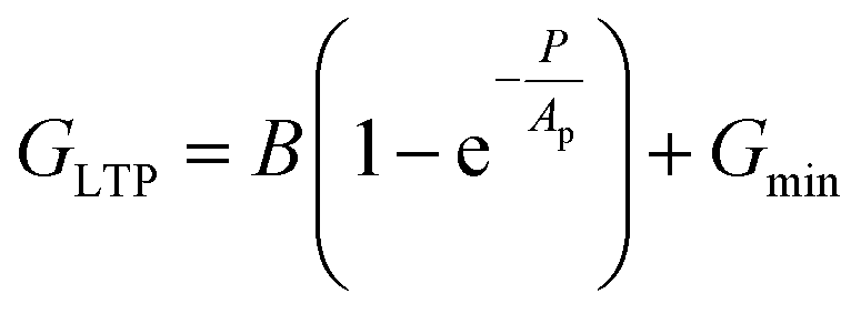 | (1) |
 | (2) |
 | (3) |
| αp,d = 1.726/(Ap,d + 0.162) | (4) |
 | ||
| Fig. 8 Schematic of the potentiation/depression pulse train waveform and LTP/LTD synaptic characteristics of (a) the pristine FeFET and (b) the plasma LAM FeFET. | ||
G LTP and GLTD represent the channel conductance for LTP and LTD, respectively. Furthermore, Gmax, Gmin, and P denote, respectively, the maximum and minimum channel conductance and the number of pulses from the experimental data. Ap,d and B are fitting parameters, and αp,d are the nonlinearity values for potentiation and depression. In Fig. 8(b), compared to the pristine FeFET, the laminated plasma FeFET demonstrates a 1.23 times lower asymmetry value, nearly double Gmax/Gmin ratio, and 25 times more states in both potentiation and depression. These results indicate that the LAM plasma FeFET exhibits more favorable characteristics for functioning as a synaptic device compared to the pristine FeFET. Additionally, it can be observed that the conductance range differs between pristine FeFET and LAM plasma FeFET. This phenomenon is due to the difference in their Vc values. Vc is the voltage required to switch the polarization of the FE layer. As shown in Fig. 3, the Vc of the LAM plasma FE is 40% higher than that of the pristine FE. As a result, when the same voltage is applied, the LAM plasma FeFET undergoes less dipole switching than the pristine FeFET, resulting in lower channel conductance.
To evaluate how the characteristics of the synaptic FeFET devices perform in system-level architecture, simulations were conducted using the NeuroSim system-level macro model based on the MNIST dataset.34 The neural network used for the simulation was a 2-layer MLP consisting of 400 input neurons, 100 hidden neurons, and 10 output neurons. The training process was conducted using a feedforward (FF) and backpropagation (BP) approach with stochastic gradient descent (SGD) as the learning method, while the classification process was performed using only the FF method (Fig. 9(a)). The simulation conducted over 40 training epochs demonstrated that the pristine FeFET achieved an inference accuracy of approximately 70%, while the laminated plasma FeFET exhibited a comparatively higher accuracy of around 80% (Fig. 9(b)). Additionally, inference accuracy fluctuation is observed to be higher in the pristine FeFET compared to the LAM plasma FeFET. This phenomenon is attributed to differences in cycle-to-cycle variation between the two devices. Cycle-to-cycle variation, also known as temporal variation, plays a critical role in determining the learning and inference accuracy of neuromorphic systems.35 This variation is closely linked to the endurance characteristics of FeFET devices. As synaptic devices undergo fatigue, their weight update properties deteriorate, resulting in greater variation over cycles. Thus, the larger fluctuation in system-level inference accuracy seen in pristine FeFETs compared to LAM plasma FeFETs can be explained by the inferior endurance characteristics of the pristine devices, as demonstrated in the simulations. Consequently, the simultaneous application of plasma treatment and laminated structure to FeFETs indicates a significant contribution to enhancing both the memory characteristics and synaptic properties of the FeFET as neuromorphic analog synaptic device.
 | ||
| Fig. 9 (a) The 2-layer MLP neural network and (b) inference accuracy of the pristine FeFET and FeFET with FE lamination and plasma treatment obtained through the NeuroSim simulation tool based on the MNIST dataset. | ||
4. Conclusion
We investigated the effects of FE lamination and fluorine plasma treatment on the performance and synaptic characteristics of HZO-based FeFETs. Our study indicates that when these techniques are applied simultaneously, they compensate for the Pr reduction and endurance degradation observed when used separately, leveraging their combined advantages. When comparing a pristine FeFET with an engineered LAM plasma FeFET, endurance characteristics improved by more than one order while maintaining the same MW at 1.2 V. Specifically, in terms of the LTP/LTD characteristics, the Gmax/Gmin ratio increased from 4 to 7, the asymmetry value decreased from 4.68 to 3.44, and the number of states increased from 75 to 100. Furthermore, simulations based on the MNIST dataset demonstrated a relatively higher inference accuracy of 80%. It was confirmed that employing both engineering techniques enhances the synaptic characteristics of FeFET-based analog synapses.Data availability
Our data in this paper are original, and can be accessed through permission from the authors.Conflicts of interest
The authors declare that they have no known competing financial interests or personal relationships that could have appeared to influence the work reported in this paper.Acknowledgements
This research was supported by the National Research Foundation of Korea (NRF) funded by the Ministry of Science, ICT & Future Planning (RS-2024-00407767, RS-2022-00154752, RS-2023-00260527). Also, this work was supported by the Technology Innovation Program (RS-2024-00509266) funded By the Ministry of Trade, Industry & Energy (MOTIE, Korea).References
- B. Sun, et al., Synaptic devices based neuromorphic computing applications in artificial intelligence, Mater. Today Phys., 2021, 18, 100393–100421 CrossRef CAS.
- W. Yue, et al., Optoelectronic Synaptic Devices for Neuromorphic Computing, Adv. Intell. Syst., 2021, 3, 1 Search PubMed.
- D. Kim, et al., Analog Synaptic Transistor with Al-Doped HfO2 Ferroelectric Thin Film, ACS Appl. Mater. Interfaces, 2021, 13(44), 52743–52753 CrossRef CAS PubMed.
- G. Indiveri and S. Liu, Memory and Information Processing in Neuromorphic Systems, Proc. IEEE, 2015, 103(8), 1379 CAS.
- O. Rhodes, Brain-inspired computing boosted by new concept of completeness, Nature, 2020, 586(7829), 364–366 CrossRef CAS PubMed.
- R. A. Nawrocki, R. M. Voyles and S. E. Shaheen, A Mini Review of Neuromorphic Architectures and Implementations, IEEE Trans. Electron Devices, 2016, 63(10), 3819–3829 CAS.
- W. Banerjee, Challenges and Applications of Emerging Nonvolatile Memory Devices, Electronics, 2020, 9(6), 1029–1052 CrossRef CAS.
- K. Huang and C. Qin, eNVM based In-memory Computing for Intelligent and Secure Computing Systems, in 2019 32nd IEEE International System-on-Chip Conference (SOCC), 2019, pp. 348–353.
- X. Sun and S. Yu, Impact of Non-Ideal Characteristics of Resistive Synaptic Devices on Implementing Convolutional Neural Networks, IEEE J. Emerg. Sel. Top. Circuits Syst., 2019, 9(3), 570–579 Search PubMed.
- P.-Y. Chen and S. Yu, Reliability perspective of resistive synaptic devices on the neuromorphic system performance, IEEE Int. Reliab. Phys. Symp. Proc., 2018, SC 4.1–SC 4.4 Search PubMed.
- M. Jerry, et al., Ferroelectric FET analog synapse for acceleration of deep neural network training, IEEE Int. Electron Devices Meet., 2017, 6.2.1–6.2.4 Search PubMed.
- M. Lederer, et al., Ferroelectric Field Effect Transistors as a Synapse for Neuromorphic Application, IEEE Trans. Electron Devices, 2021, 68(5), 2295–2300 CAS.
- H. Mulaosmanovic, et al., Novel ferroelectric FET based synapse for neuromorphic systems, Symp. VLSI Technol., 2017, T176–T177 Search PubMed.
- B. Ku, Y. Shin, Y. Lee, T. Kim and C. Choi, Improved ferroelectric characteristics of ALD lanthanum-doped hafnium oxide thin film by controlling post-cooling time, Appl. Surf. Sci., 2022, 599, 153905–153911 CrossRef CAS.
- B. Ku, Y.-R. Jeon, M. Choi, C. Chung and C. Choi, Effects of post cooling on the remnant polarization and coercive field characteristics of atomic layer deposited Al-doped HfO2 thin films, Appl. Surf. Sci., 2022, 601, 154039–154048 CrossRef CAS.
- H. K. Peng, C. Y. Chan, K. Y. Chen and Y. H. Wu, Enabling large memory window and high reliability for FeFET memory by integrating AlON interfacial layer, Appl. Phys. Lett., 2021, 118(10), 103503–103506 CrossRef CAS.
- Y.-R. Jeon, D. Kim, B. Ku, C. Chung and C. Choi, Synaptic Characteristics of Atomic Layer-Deposited Ferroelectric Lanthanum-Doped HfO2 (La:HfO2) and TaN-Based Artificial Synapses, ACS Appl. Mater. Interfaces, 2023, 15(49), 57359–57368 CAS.
- K. A. Aabrar, et al., BEOL-Compatible Superlattice FEFET Analog Synapse With Improved Linearity and Symmetry of Weight Update, IEEE Trans. Electron Devices, 2022, 69(4), 2094–2100 CAS.
- A. Tarek, et al., Impact of the Ferroelectric Stack Lamination in Si Doped Hafnium Oxide (HSO) and Hafnium Zirconium Oxide (HZO) Based FeFETs: Toward High-Density Multi-Level Cell and Synaptic Storage, Electron. Mater., 2021, 2(3), 344–369 CrossRef.
- T. Ali, et al., A Multilevel FeFET Memory Device based on Laminated HSO and HZO Ferroelectric Layers for High-Density Storage, IEEE Int. Electron Devices Meet., 2019, 28.7. 1–28.7. 4 Search PubMed.
- Y. Choi, H. Park, C. Han and C. Shin, Impact of CF4/O2 Plasma Passivation on Endurance Performance of Zr-Doped HfO2 Ferroelectric Film, IEEE Electron Device Lett., 2023, 44(5), 713–716 CAS.
- Y. Choi, H. Park, C. Han, J. Min and C. Shin, Improved remnant polarization of Zr-doped HfO2 ferroelectric film by CF4/O2 plasma passivation, Sci. Rep., 2022, 12(1), 1–7 CrossRef PubMed.
- S. Riedel, P. Polakowski and J. Müller, A thermally robust and thickness independent ferroelectric phase in laminated hafnium zirconium oxide, AIP Adv., 2016, 6, 9 Search PubMed.
- G. Park, et al., Tailoring of Ferroelectric Coercive Field and Polarization With Ferroelectric and Antiferroelectric HfxZr1−xO2 Bilayer Structure, IEEE Electron Device Lett., 2024, 45(10), 1997–2000 CAS.
- P. Buragohain, et al., Fluid Imprint and Inertial Switching in Ferroelectric La:HfO 2 Capacitors, ACS Appl. Mater. Interfaces, 2019, 11(38), 35115 CrossRef CAS PubMed.
- J. Chen, et al., Impact of Oxygen Vacancy on Ferroelectric Characteristics and Its Implication for Wake-Up and Fatigue of HfO2-Based Thin Films, IEEE Trans. Electron Devices, 2022, 69(9), 5297–5301 CAS.
- Y. Zhou, et al., The effects of oxygen vacancies on ferroelectric phase transition of HfO2-based thin film from first-principle, Comput. Mater. Sci., 2019, 167, 143–150 CrossRef CAS.
- X. Ke, et al., Switching Dynamics of HfO2−ZrO2 Nanolaminates With Different Laminate Thicknesses, IEEE Trans. Electron Devices, 2024, 71(6), 3651–3658 CAS.
- C. S. Lai, K. M. Fan, W. C. Wu, J. C. Wang and S. J. Lin, Effects of post CF4 plasma treatment on the HfO2 thin film, Jpn. J. Appl. Phys., Part 1, 2005, 44(4B), 2307 CrossRef CAS.
- C. Kim, D.-O. Kim and W. Y. Choi, Influence of gate-source/drain overlap on FeFETs, Solid-State Electron., 2024, 214, 108862–108865 CrossRef CAS.
- M. H. Park, et al., Study on the internal field and conduction mechanism of atomic layer deposited ferroelectric Hf0.5Zr0.5O2 thin films, J. Mater. Chem. C, 2015, 3(24), 6291 RSC.
- W.-C. Wu, et al., Fluorinated HfO2 gate dielectrics engineering for CMOS by pre- and post-CF4 plasma passivation, in 2008 IEEE International Electron Devices Meeting, Electron Devices Meeting, 2008, IEDM 2008. IEEE International, 2008, vol. 1 Search PubMed.
- S. Kuk, S. Han, B. H. Kim, S. Baek, J. Han and S. Kim, An Investigation of HZO-Based n/p-FeFET Operation Mechanism and Improved Device Performance by the Electron Detrapping Mode, IEEE Trans. Electron Devices, 2022, 69(4), 2080–2087 CAS.
- Y. Luo, X. Peng and S. Yu, MLP + NeuroSimV3.0: Improving On-chip Learning Performance with Device to Algorithm Optimizations, in Proceedings of the International Conference on Neuromorphic Systems, 2019, pp. 1–7.
- P. Y. Chen, et al., Mitigating effects of non-ideal synaptic device characteristics for on-chip learning, in 2015 IEEE/ACM International Conference on Computer-Aided Design (ICCAD), 2015, pp. 194–199.
| This journal is © The Royal Society of Chemistry 2025 |