
Determination of the carrier temperature in weakly confined semiconductor nanocrystals using time-resolved optical spectroscopy†
Ivo
Tanghe
 *abc,
Chao-Yang
Lin
defg,
Isabella
Wagner
de,
Margarita
Samoli
a,
Servet
Ataberk Cayan
ab,
Zeger
Hens
ab,
Justin
Hodgkiss
de,
Kai
Chen
defg and
Pieter
Geiregat
ab
*abc,
Chao-Yang
Lin
defg,
Isabella
Wagner
de,
Margarita
Samoli
a,
Servet
Ataberk Cayan
ab,
Zeger
Hens
ab,
Justin
Hodgkiss
de,
Kai
Chen
defg and
Pieter
Geiregat
ab
aPhysics and Chemistry of Nanostructures, Ghent University, 9000 Ghent, Belgium. E-mail: ivo.tanghe@ugent.be
bNoLIMITS Center for Non-Linear Microscopy and Spectroscopy, Ghent University, 9000 Ghent, Belgium
cPhotonics Research Group, Ghent University, 9000 Ghent, Belgium
dSchool of Chemical and Physical Sciences, Victoria University of Wellington, Wellington, New Zealand
eMacDiarmid Institute for Advanced Materials and Nanotechnology, Wellington, New Zealand
fThe Dodd-Walls Centre for Photonic and Quantum Technologies, University of Otago, Dunedin, New Zealand
gRobinson Research Institute, Victoria University of Wellington, Wellington, New Zealand
First published on 6th January 2025
Abstract
Many applications of nanocrystals rely on their use in light detection and emission. In recent years, nanocrystals with more relaxed carrier confinement, including so-called ‘bulk’ and 2D implementations, have made their stake. In such systems, the charge carriers generated after (photo-)excitation are spread over a semi-continuous density of states, behaviour controlled by the carrier temperature T. Current established methods to measure this dynamically changing temperature include transient absorption and luminescence spectroscopy, yet they very often fail to agree on the exact temperature leading to contradicting reports. Here, we show through a combined side-by-side experimental and theoretical study on state-of-art II–VI and perovskite nanocrystals under weak confinement that only transient PL can yield unambiguously the correct T. In particular, temperatures extracted from TA are heavily affected by the effective masses of the electron and hole bands involved leading to overestimations. Our results pave a way to a more robust extraction of carrier temperature and will help to consolidate ensuing structure–property relations derived from it.
1 Introduction
In recent years, several high quality direct gap semiconductors have been synthesized through low cost methods, such as colloidal synthesis or solution phase epitaxy. In particular weakly confined materials structured on the nanoscale, such as 2D and 3D perovskite films,1,2 but also weakly confined II–VI quantum dots, quantum shells and nano-platelets, have shown great potential for both solution processable lasers, light emitting diodes, displays and photovoltaics.3–8The distribution of charge carriers generated through photo-excitation over the semi-discrete, often even nearly continuous, energy spectrum of these materials is a key parameter to evaluate and optimize their performance in such devices. For example in the context of photovoltaics, the extraction of carriers with excess energy, so-called ‘hot carriers’, relative to the band gap is highly desired to boost the efficiency.9,10 In such cases, it is paramount to know the effect of composition and shape of the semiconductor on both the efficiency of generating hot charges and the timescales on which they cool down, i.e. redistribute to lower energy states. A case example explored extensively in the past years is that of halide-perovskite semiconductors. Several groups have shown that the A-site cation has a critical role in slowing down carrier relaxation, highlighting for example differences between MAPbBr3 and CsPbBr3.11–17 Other reports showed that also the B-site can be of importance, showing evidence of a remarkable cooling bottleneck in Sn-trihalide perovskites.18–20
For those applications involving net optical gain, such as super-luminescent diodes (SLEDS) or lasers, the balance between stimulated emission and absorption is also heavily affected by the distribution of charges over the energy spectrum. Indeed, a strongly diluted occupation of the band edge states leads to problems in sustaining the required population inversion and/or obtaining the maximum gain coefficients, a well-known issue in epitaxially grown semiconductor lasers.1,7 On the other hand, spreading out carriers over high energy states can be beneficial to obtain spectrally broadband lasing from a single material as indicated recently with weakly confined quantum dots, so-called ‘bulk nanocrystals’.21,22 Clearly, the detailed knowledge of the distribution n(E) of charges over an energy level spectrum of a semiconductor is highly desired. If the energy levels are closely spaced, said distribution is dictated by the temperature T of the electron (n) and/or hole (p) gas after photo-excitation, i.e. n(E,T), as shown in Fig. 1a for a continuous parabolic energy band for varying temperatures from 300 K to 4000 K. Close to room temperature, here taken as 300 K, charges tend to condense to the bottom of the energy band, highly desirable for optical gain, whereas at higher carrier temperatures the spread to higher energy is clearly noticeable, a more favorable situation for hot carrier extraction. We note that this temperature relates to the carrier temperature, not the lattice temperature of the material. As the cooling and thermalization dynamics often proceed on very fast timescales, the toolbox of interest to obtain the carrier temperature T is that of contact-free ultrafast optical spectroscopy methods, such as transient absorption (TA)13,17,23–27 and, somewhat less used in literature, femtosecond broadband photoluminescence (PL).16,28–30 Using these increasingly available techniques, researchers have attempted to extract T by measuring the transient occupation of the energy bands n(E,T). This occupation is evaluated by analyzing the tail of either the TA bleach signal or the PL intensity at high photon energies, i.e. above the optical band gap. To the high energy slope of such traces, a simple exponential decay is fitted, from which a temperature is extracted under the approximation that the measured signals are  . However, it remains rather unclear whether this ‘Boltzmann tail’ (BT) approach is correct and which of the commonly used methods, TA and/or PL, now yields a correct and consistent carrier temperature T, as extracted from such a fit. Moreover, it is also unclear under which circumstances these all-optical methods would agree on the exact temperature. Claims on carrier cooling bottlenecks and excessive overheating of the carrier gas, are therefore not always substantiated by solid theoretical background for both the experimental, and ensuing fitting, method used.13,24,25
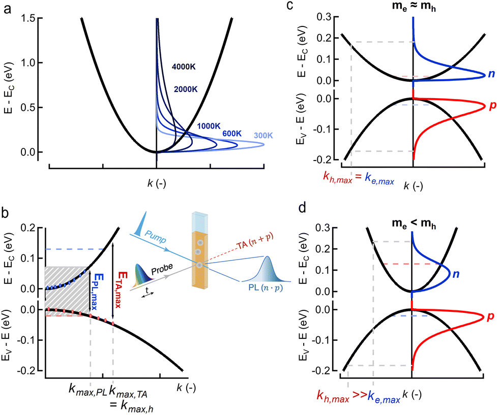 | ||
Fig. 1 (a) Carrier distribution functions n(E,T) (blue shades) for different carrier temperatures T from 300 K to 4000 K for a simple parabolic energy band (black). (b) Overview of ultrafast optical methodologies where a pump excites the colloidal dispersion and consequently a change in probe transmission (absorption) is measured in TA (red) and the emitted (spontaneous) photoluminescence (PL, blue). Graph shows the maximum energies probed by transient photo-luminescence (PL) and transient absorption (TA) between a valence band (bottom black) and conduction band (top black), and the associated maximum k-vectors, showing clearly that kmax,TA > kmax,PL and associated energies ETA,max > EPL,max. Note that for this band-asymmetric situation with a hole mass exceeding the electron mass (smaller curvature), the holes (red dots) extend much further in k-values than the electrons (blue dots). (c and d) Conduction and valence bands of a symmetric (c, 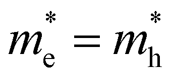 ) and asymmetric (d, ) and asymmetric (d, 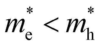 ) energy band situation, showing in parallel the electron (blue, n(E)) and hole (red, p(E)) distribution functions for the same carrier temperature T and total carrier density ) energy band situation, showing in parallel the electron (blue, n(E)) and hole (red, p(E)) distribution functions for the same carrier temperature T and total carrier density 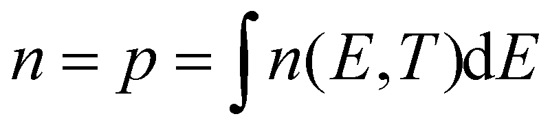 . Horizontal axis shows the maximum k vector of occupied electron (blue) and hole (red) states. . Horizontal axis shows the maximum k vector of occupied electron (blue) and hole (red) states. | ||
Here, we show by combining theoretical modeling with a joint ultrafast TA/PL study on the same state-of-art materials, i.e. green emitting CsPbBr3 perovskites and II–VI CdS bulk nanocrystals, under identical conditions (excess energy, carrier density, …) that TA consistently overestimates the temperature if a simple direct single exponential tail fit is used. Opposed to this, PL consistently produces correct a temperature within this formally most simple approach. Introducing a theoretically predicted correction factor based on the band curvatures (i.e. effective masses), we can however make both methods agree better. Applying this improved methodology to both band-symmetric (perovskite) and band-asymmetric (CdS) scenarios, we further identify that despite the now reasonably good agreement, TA is still much more sensitive to the higher energy band structure of the semiconductor, thereby complicating the analysis further. These observations make us conclude that time- and energy-resolved PL is the more reliable method to extract carrier temperatures in (weakly confined) semiconductor nanocrystals.
2 Carrier temperature
We first discuss what temperature imparts on a direct band gap semiconductor's properties and how it could be extracted from optical experiments. Fig. 1a already showed how the temperature T of charge carriers affects their distribution function n(E,T) over the energy level spectrum, here represented by a parabolic energy band with fixed effective mass m*. The spreading of charge carriers is controlled by the temperature T through the Fermi–Dirac distribution f(E,T,Ef,e), resulting for example for electrons (n,‘e’) and holes (p,‘h’) in: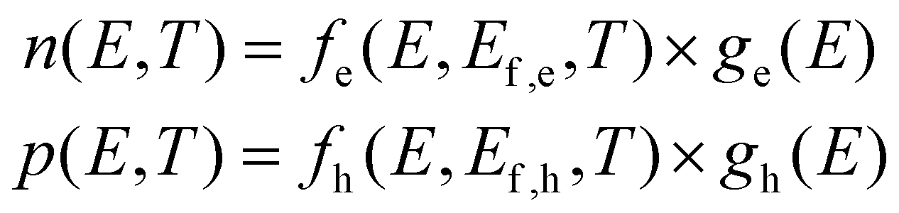 | (1) |
In line with this idea, spectrally resolved optical methods attempt to probe these carrier distributions (n,p)(E) but always do so simultaneously as optical excitation generates an equal total amount of electrons and holes right after photo-excitation, i.e.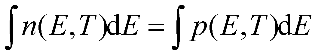 . This happens either as a sum n + p, in frequently used transient absorption (TA) experiments, or a product n × p, in photoluminescence (PL) experiments, see Fig. 1b. Indeed, in TA a bleach ΔA(E) < 0 of the probe absorption is observed as soon as carriers block an optical transition after photo-excitation. This means that both an electron or a hole can cause a signal, see Fig. 1b. Even if no electrons are present at high k-values, a probe beam can still detect the presence of the spread out holes at higher cut-off energies. In ultrafast PL experiments, the sample is excited with a short light pulse and the (spontaneously) emitted light after electron–hole pair recombination is detected. The latter is proportional to the product n × p, see Fig. 1b, as it requires the presence of both charges in a vertical, momentum-conserving, transition. This implies that a much narrower spread in k-values is sampled by PL compared to TA. This results in a narrower energy range probed in PL for a similar carrier density, ΔEPL,max < ΔETA,max as indicated in Fig. 1b by the blue and red vertical lines. Clearly, TA and PL measure the carrier distribution functions in different ways, thereby making the concept of a universal fitting method rather unlikely.
Breaking the formulas for n, p from above further down into their constituent elements, we can discuss the role of the Fermi–Dirac factors fe,h and the DOS separately and get a further impression of possible difficulties to reliably extract a temperature. First, the occupation factors fe,h underpinning n and p are a complex function of energy and temperature. To tackle this, one often uses a shortcut based on the assumption that the Fermi–Dirac distribution approximates a much simpler Boltzmann-type expression (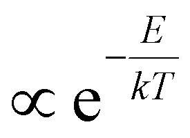 ) at high energy relative to the Fermi level Ef. Combined with the assumption of a flat density of states g(E) for those energies, one therefore typically approximates n(E,T) as a decaying single exponential function whose slope is proportional to 1/T. Based on this ‘Boltzmann Tail’ (BT) approximation, the rough extrapolation is then made that both TA and PL signals at high energy reveal the temperature by a simple exponential fit whose slope scales with 1/T, the methodology described in the introduction:
 | (2) |
Clearly, such a single exponential approximation is a shortcut as neither TA, nor PL, measures n or p separately, but rather as a sum (TA) or product (PL). As mentioned, it is not clear which method is able to come closer to the formal shape of the BT approximation and under which conditions this might hold.
Finally, taking a look at the DOS factor in the expressions above, we note that a good knowledge of this DOS boils down to the effective mass m* (or curvature) of the energy band involved, a number often well-known for electrons in popular III–V and II–VI semiconductors, but typically less so for holes. Moreover, as mass represents band curvature, the non-parabolic nature of energy bands at higher energies away from the fundamental gap might pose a second problem, which can be seen as an energy dependent effective mass m*(E). To better understand the impact of the band structure, Fig. 1c and d sketch a situation of carrier spreading for the same total carrier density and temperature, but where the mass of electrons is either comparable to, or smaller than, the hole mass respectively in Fig. 1c and d. The effective mass clearly has a large impact on the distribution of charges over energy as shown by the red (electrons) and blue (holes) curves. It remains unclear to date how this affects TA or PL experiments, and the eventual extraction of a consistent carrier temperature.
3 Experimental results
Already a first discussion of TA and PL methodology laid out above to extract T indicated possible pitfalls in comparing both methods. To this end, we first present results of TA and PL experiments carried out on the same samples under the same pumping conditions (wavelength, excess energy of pump, generated carrier density). Fig. 2 shows an overview of the optical properties of two bulk-like reference systems with direct and quite comparable band gaps, yet very different band symmetries: CdS bulk nanocrystals (12 nm diameter, band gap at 517 nm), used to showcase disruptive broadband lasing in earlier works,7 with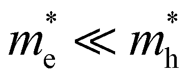 (top row, Fig. 2), and a typical halide perovskite system, CsPbBr3 bulk nanocrystals (10 nm diameter, band gap at 550 nm), with
 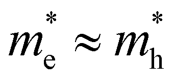 (bottom row, Fig. 2).31,32 In both cases the nanocrystals have sizes exceeding the Bohr diameter leading to a quasi-continuous density of states for electrons and holes.7,32–34 The synthesis description and basic optical characterization are given in ESI S1,† including the normalization procedure to represent the absorption as the intrinsic absorption coefficient μi,0. As a case example, the remaining tabs of Fig. 2 show the raw experimental 2D data-sets obtained for both samples in a joint TA (red, showing ΔA)/PL(blue, showing collected photons as counts) experiment after a common 400 nm excitation creating a carrier density around n ≈ 2.0 × 1019 cm−3.
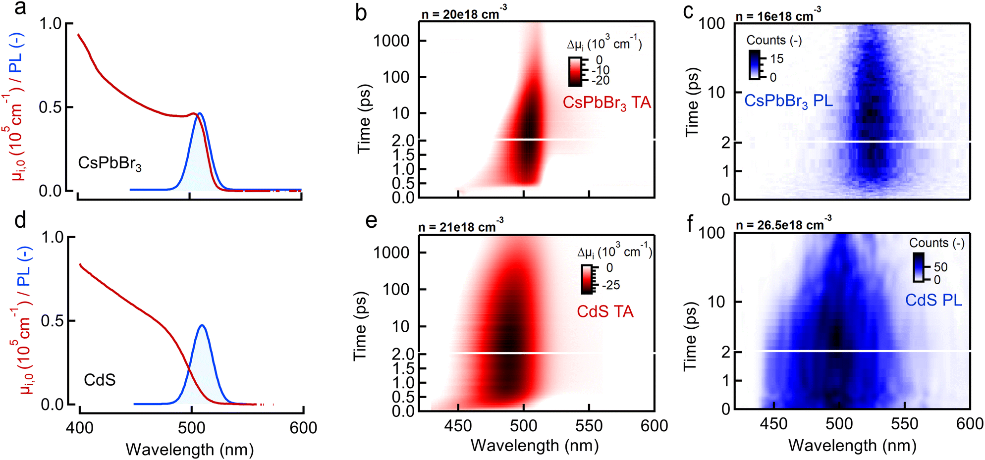 | ||
| Fig. 2 Sample and experimental data overview (a) linear absorption spectra (red) of CsPbBr3 (top) and (d) CdS (bottom) bulk nanocrystals and corresponding steady state photoluminescence (PL, blue) after 400 nm excitation. (b and e) Color maps show the resulting ΔA(λt) transient absorption (TA) (red) and (c and f) transient PL(λt) (blue) maps for approximately the same generated carrier density created after 400 nm excitation. Carrier densities are chosen relatively close together around a value of n = 2.0 × 1019 cm−3 at time zero. | ||
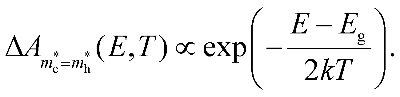
Starting from these data-sets, reported more extensively in ESI S2,† we proceeded to extract the TA/PL signal as function of probe/PL energy for various pump fluences based on the single exponential tail fit (or BT approximation) model used in literature, at different delay times after photo-excitation at time zero. As shown in the ESI,† fitting a single exponential decay to the high energy tail yields a set of temperatures T plotted in Fig. 3a, b (perovskite) and Fig. 3c, d (CdS) for both samples as function of time after photo-excitation. In both cases the discrepancy between TA (red) and PL (blue) becomes very clear when plotting the extracted temperature at 3 ps delay, as an example, in Fig. 3e and f. We choose 3 ps as a time where thermalization of the electron and hole gas allow to both define a temperature T and assume Te = Th. Despite both methods agreeing on an increasing temperature with carrier density, the TA approach (red) yields consistently higher temperatures and slower temperature relaxation dynamics, compared to PL (blue) for both samples. We also observe that the PL temperature naturally evolves back to the expected limit of room temperature (300 K) whereas the TA seems to level of at a higher value of ca. 600 K. The top graph in Fig. 3e and f shows the ratio of the TA temperature to the PL temperature. Clearly, the often used single exponential approximation fails to agree on the carrier temperature after photo-excitation resulting in an over-estimation of the temperature by a factor of 2 to 3 in TA depending on the sample. Moreover, the temperatures extracted from PL match better to the room temperature limits (ca. 300 K) at low density, whereas the TA analysis overshoots this expected limit by a factor of ca. 2.
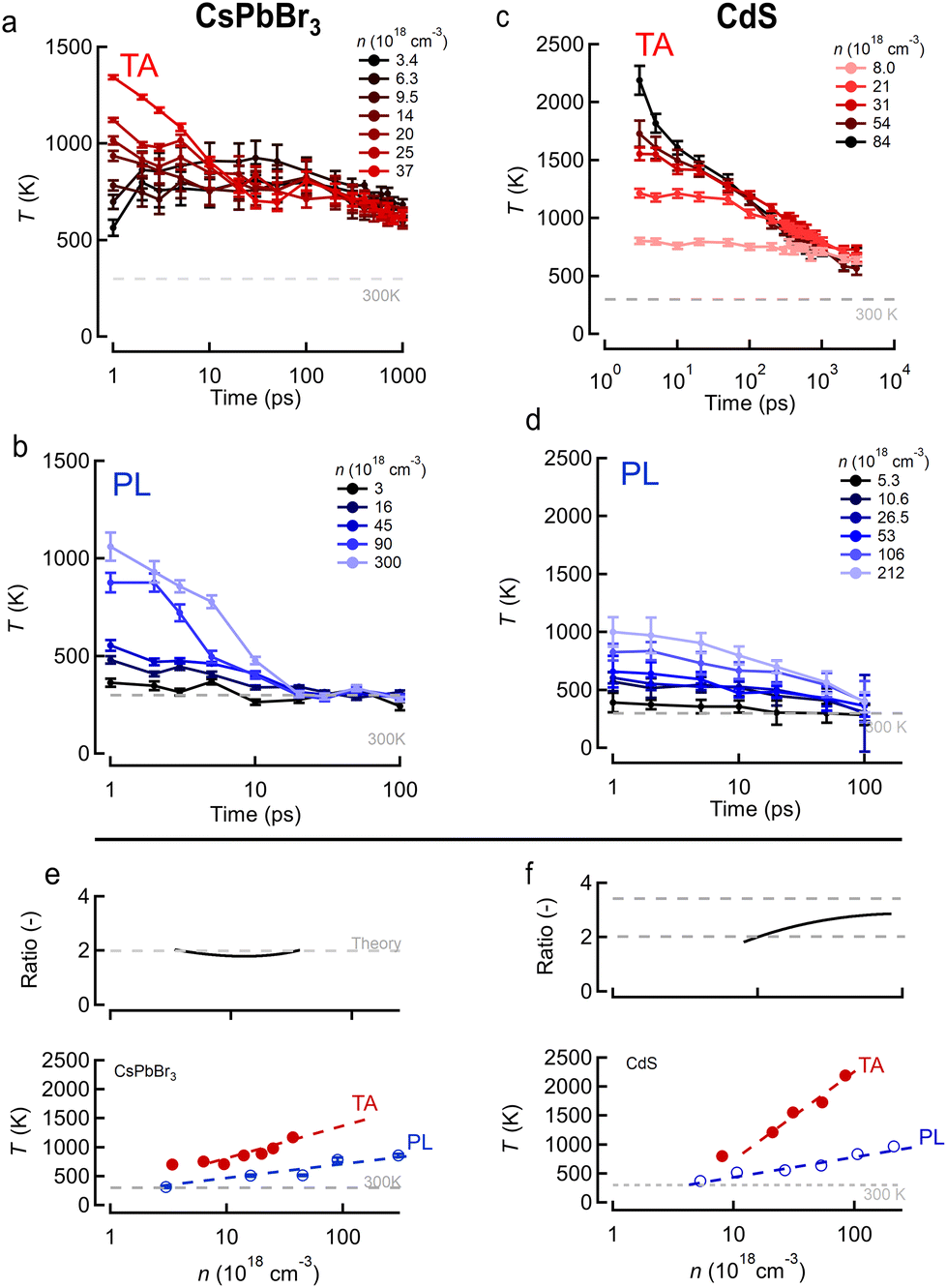 | ||
| Fig. 3 Joint transient absorption (TA, red) and transient PL (blue) experiments on perovskite (CsPbBr3, left column) and CdS nanocrystals (right column). (a and c) Extracted carrier temperature from TA experiments on (a) perovskite and (c) CdS after 400 nm excitation. (b and d) Extracted carrier temperature from transient PL experiments on (b) perovskite and (d) CdS for similar 400 nm excitation. (e and f) Temperature at 3 ps delay with pump from TA (red) and PL (blue) for increasing carrier densities n for the (e) perovskite and (f) CdS samples. Top graphs show the ratio of TA to PL temperatures, black curve, together with a theory prediction (see further) in grey dashed lines. | ||
4 Theoretical model and interesting limits
To understand the discrepancies observed experimentally with the single exponential (or BT) approximation applied universally to both TA and PL, we take one step back to write down a theoretical basis by looking at the formal expressions for the signals observed in the latter experiments. Doing so, we deduce in particular how temperature is incorporated without any assumptions a-priori. Starting out with the most common methodology of TA, we can write the measured ΔA at a given time delay t, which will be omitted for clarity further on, as:| ΔA(E,T) = A(E,T) − A0(E) = (fh(E,T) − fe(E,T) − 1)A0(E) | (3) |
 for a 3D semiconductor. For a detailed explanation, we refer to ESI S3.† In line with this, we can write the photoluminescence PL(E) as follows:
| PL(E,T) = C·fe(E,T)·(1 − fh(E,T))·ge,h(E). | (4) |
Using the approximation that the respective carrier energies probed are much higher than the associated quasi-Fermi levels, a situation we refer to as the high energy limit, we can also write these factors in a more compact form. ESI S3† and Fig. 4 discuss in detail how valid this high energy limit is, see also further in the Discussion section. As derived formally in the ESI,† the occupation factors in this high energy probe limit for the conduction (e) and valence bands (h) are given by:
 | (5) |
 | (6) |
 ,
,  the effective electron and hole masses, Eg the optical band gap and the reduced mass
  . The pre-factors Ce,h(T) are a function of temperature and related to the quasi-Fermi level positions. However, since they do not contain any energy dependence, we can treat these effectively as fit parameters when fitting traces on an energy scale. Continuing in the acceptable high energy limit, we find based on the expressions of eqn (3) and (4):
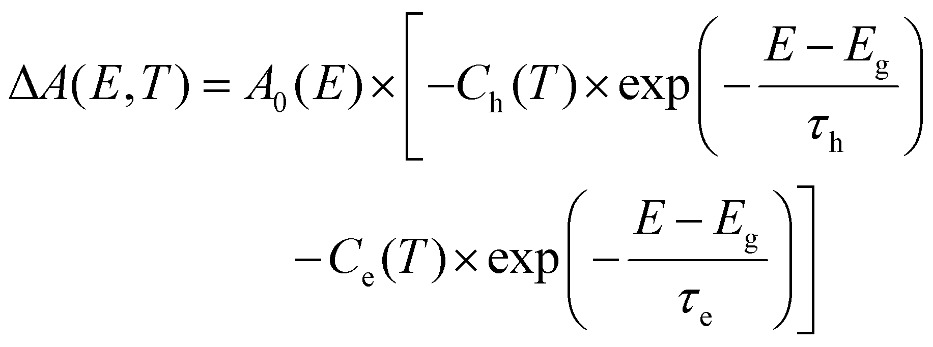 | (7) |
 | (8) |
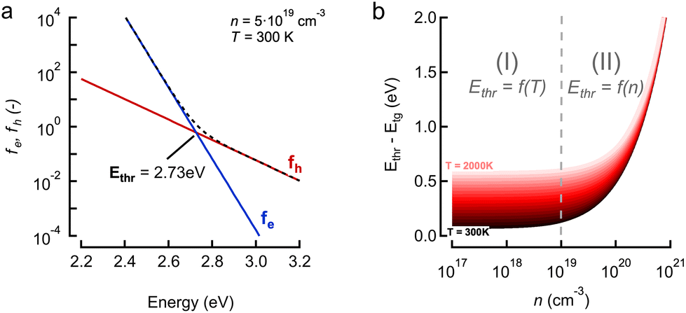 | ||
| Fig. 4 Discussion on the theory model and fitting range. (a) Role of electron (e, red) and hole (h, blue) occupation factors as function of energy. Note that for this combination of (n,T) = (5 × 1019 cm−3 300 K) the tipping point where the holes become dominant is labeled as Ethr = 2.73 eV. (b) Plot of Ethr relative to the band gap energy Eg, as Ethr − Eg, for increasing density n and temperature T (shaded reds). We can identify 2 regimes, regime (I) at low density, ca. <1019 cm−3, where the threshold varies linearly with temperature T and does not depend on n. At higher densities the curves for different T converge in a second regime (II) where the threshold only depends on density as Ethr ∝ n2/3. | ||
Here, 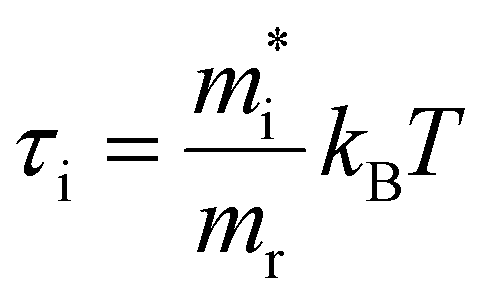 for i = e, h contains the temperature T but with a scaling parameter depending only on the masses of the carriers. Already a few crucial observations can be made at this point where only a high-energy limit is taken. For TA, a sum of two exponentials is obtained which deviates from the notion of a single exponential, the essence of the tail approximation often used, a point we will come back to further. Second, the slope of these curves is dictated by a mass ratio times the temperature, making the extraction of T dependent on the exact knowledge of the mass. Moreover, the weight factors of these two exponentials seem to be temperature dependent. As laid out in ESI S3.3,† a closer look at the TA eqn (7) shows that for carrier densities n < 1020 cm−3, a quite typical range for a photo-excited semiconductor, the pre-factors Ce and Ch can be simplified to yield an even more insightful expression of the TA signal:
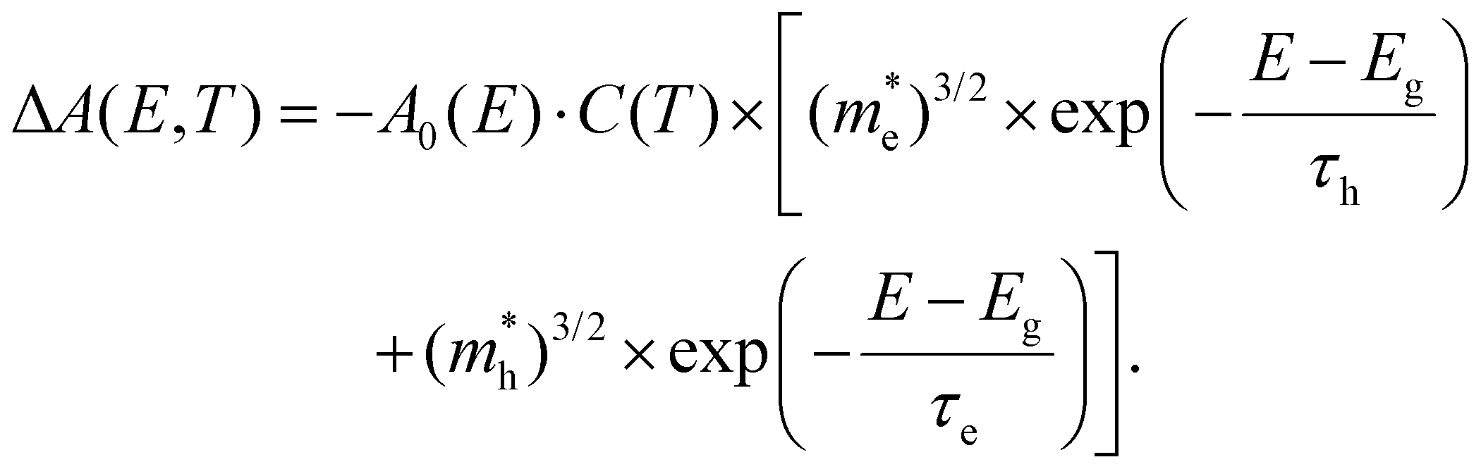 | (9) |
For the case that  , found e.g. in most II–VI and III–V systems including the CdS studied here experimentally, we can appreciate that the second, light-mass (electron) related, exponential will decay much quicker although it has a higher initial weight since τe ≪ τh, as is shown in Fig. 4a. As a result, the fits at high energy are dominated by holes, see also Fig. 4a:
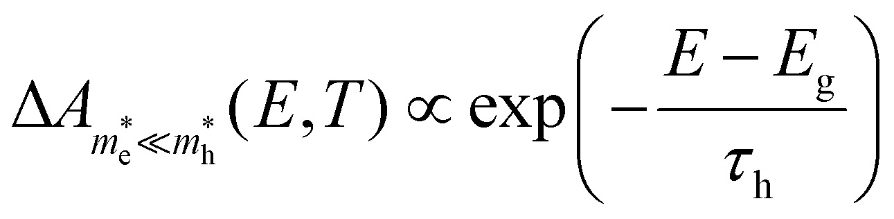 | (10) |
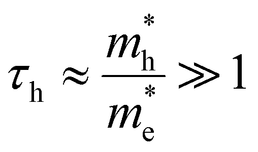 . Looking back at Fig. 1b, this is exactly what could be expected as the heavier holes spread out much more in momentum space, resulting in their sole contribution to the TA signal at high probe photon energies. Eqn (10) is exactly what the often used single exponential decay approximation would produce, yet the temperature is now scaled with a factor τh ≫ 1. Again, this is quite a general result as it holds for a wide range of photon energies and carrier densities n < 1020 cm−3, see further.
For the case where the masses of both electron and hole are more equal, e.g. for CsPbBr3 where  ,31eqn (9) simplifies since τh = τe = 2kBT and Ce = Ch, resulting in the quite simple expression:
 | (11) |
This expression again mimics the BT approximation of a single exponential decay, but the slope is now dictated by 2kBT, not kBT.
Summarizing the above, we can conclude that for TA formally a single exponential decay approximation at high photon energy could be correct, but that the interpretation of the slope towards T is very much subject to the details of the band structure and depends strongly on the effective masses (in a given energy range). The latter becomes even more problematic for non-parabolic scenarios often found at higher energies in the band structure. In contrast to TA, the expression for the PL(E,T) in eqn (8) is rather insensitive to these problems (i.e. double exponential behaviour, required knowledge of mass, sensitivity to non-parabolicity) and always yields a single exponential decay at high energy with a direct scaling of the slope to temperature T without correction factors. As such, no a priori knowledge of band structure (mass) is needed for PL analysis. Moreover, where TA signals are often a mix of counter-acting photo-induced absorption (ΔA > 0), typically originating from shifts or band gap renormalization,7,35 and bleach (ΔA < 0), PL should offer much more straightforward signals from the start.
5 Discussion
Building on the theoretical framework laid out above, we can now take a second look at the experimental results shown earlier in Fig. 3. We expect that the PL temperatures extracted with a single exponential fit are correct and that the TA temperatures need to be corrected based on an appropriate scaling factor. Fig. 3e and f show in the top graphs (black lines) the ratio between TA and PL temperature as extracted from single exponential fits assuming the slope is dictated by 1/T. We find a scaling factor of 2 ± 0.2 for CsPbBr3, perfectly in line with theory prediction for (or τ = 2kBT) from eqn (11). This shows that for band-symmetric materials, the TA gives an equally good descriptor of carrier temperature based on a single exponential decay fit, yet only if appropriate interpretation of the energy slope is used.
For CdS however, taking typically reported values 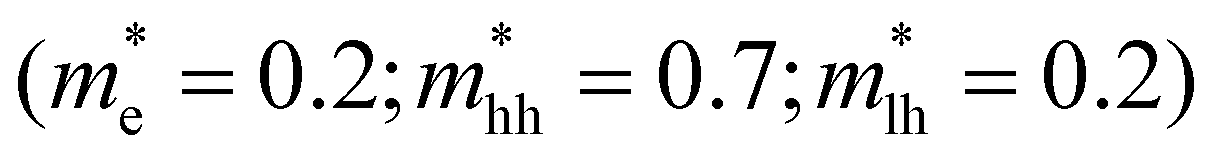 the scaling factor
 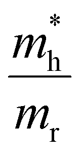 would amount to a range of 2.0 to 3.0, as indicated by the horizontal dashed lines Fig. 3f (top). However, we find experimentally that a factor of 2.0 to 2.5 is needed, see Fig. 3f (top) solid black line. Such a discrepancy can be assigned to the large uncertainty on hole masses, in particular at higher energies in the band structure of CdS. Such uncertainty is typical and arises from effective masses being reported from different approaches, beit experimentally determined through transport or optical experiments and/or theoretically calculated from semi-empirical and/or ab initio methods. This heavy reliance on a rather ill-defined parameter, again points to the situation that at high energies, or equivalently carrier temperatures, TA falls short to allow an easy determination of T.
We note that in our particular perovskite system, the carrier temperature falls back to room temperature after ca. 20 ps when evaluated properly through either PL, or rescaled TA, analysis – see e.g.Fig. 3b. This indicates that longer term overheating effects such as Auger heating36,37 or a phonon conversion bottleneck25 are not really observed for our samples. In contrast, CdS does show a lingering higher carrier temperature, see e.g.Fig. 3d.
Finally, we should comment on the ‘high energy’ limit approximation used throughout the paper. This limit relates to defining a range of energies where the conclusions made above hold, i.e. a mathematical approximation of a single exponential decay for both TA and PL, albeit with the need for a correct interpretation of the slope in both cases. More specifically, it relates to the need to define a starting energy Ethr for the tail fit where both TA and PL would give a single exponential decay. This point is exactly what is indicated on Fig. 4a as 2.73 eV for this specific combination of (n,T). As shown in ESI S3† and Fig. 4b, we can deduce this tipping point Ethr analytically as:
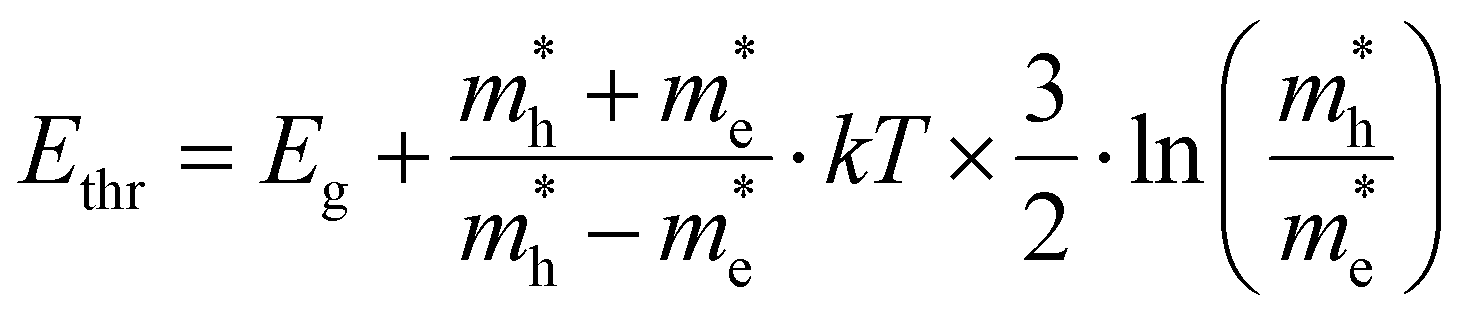 | (12) |
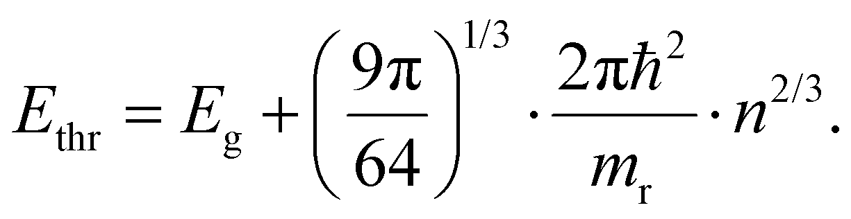 | (13) |
We note that in most experiments n remains in the range of 1017–1019 cm−3 with the lower bound found in photo-voltaic scenarios, and the higher limit found in research related to stimulated emission and band inversion scenarios.21,22 This regime is indicated by the vertical dash line in Fig. 4b, in which the threshold is a function of the temperature T itself. However, even for very high carrier temperatures up to 2000 K one can say that fitting 0.5 eV above the band gap energy is a very safe regime to keep the single exponential tail fit valid, beit again with the caveat of correctly interpreting the slope coefficient towards a temperature. In summary, we can confidently state that our conclusions are quite generally applicable to many scenarios if care is taken to adjust the energy fit range properly.
6. Conclusions
We conclude that despite the large window where a single exponential fit is applicable to TA and PL data, only PL yields the temperature of a carrier gas directly without any assumptions on band curvature. To obtain the correct temperature from a fit to TA spectra one has to explicitly take the band curvature (masses) of the charge carriers into account to avoid an overestimation of the temperature. Where the models developed here assume a continuous density of states (DOS) they can also be extended to include a 2D density of states, or even fully discrete energy levels in 0D systems, which changes little to the conclusions above. Indeed, the approximations are made at the level of the distribution functions and their energy dependence, not the DOS. As a case example, Tanghe et al. included a temperature in the description of optical gain characteristics in weakly confined CdSe/CdS quantum dots showing that coming a discrete DOS with a Fermi–Dirac occupation is a workable hypothesis.21 Our results provide a clear basis to analyze carrier temperatures and their dynamics in increasingly prevalent weakly confined, yet still nano-structured, materials, and indicate clearly that transient PL is the better option to obtain consistent results.Author contributions
I. T. and S. A. C. carried out the transient absorption experiments. C-Y. L. carried out the femtosecond PL experiments with support of K. C. and I. W. M. S. synthesized the nanocrystals. J. H. and Z. H. aided in conceptualization, reviewed the manuscript and secured funding acquisition. I. T. took charge of the theoretical methodology, the writing and the visualization. P. G. provided funding, support for the methodology development and wrote the manuscript.Data availability
The data supporting this article have been included as part of the ESI.†Conflicts of interest
There are no conflicts to declare.Acknowledgements
P. G., Z. H. and S. A. C. acknowledge support from FWO Vlaanderen through grant no. G037221N, G0B2921N and no. S0002019N. I. T. acknowledges support from the IOF through a STAR-TT project QDLASER. C. Y. Lin and K. C. acknowledge support from the Marsden Fund by the Royal Society of New Zealand through contract 23-VUW-144. P. G. acknowledges further support from H2020-ERC STG “NOMISS” Grant agreement no. 101077526 and the Core Facility program at UGent.References
- B. R. Sutherland and E. H. Sargent, Perovskite Photonic Sources, Nature Publishing Group, 2016, vol. 10, pp. 295–302 Search PubMed.
- Q. A. Akkerman, G. Rainò, M. V. Kovalenko and L. Manna, Nat. Mater., 2018, 17, 394–405 CrossRef CAS PubMed.
- D. Harankahage, J. Cassidy, J. Beavon, J. Huang, N. Brown, D. B. Berkinsky, A. Marder, B. Kayira, M. Montemurri, P. Anzenbacher, R. D. Schaller, L. Sun, M. G. Bawendi, A. V. Malko, B. T. Diroll and M. Zamkov, J. Am. Chem. Soc., 2023, 145, 13326–13334 CrossRef CAS PubMed.
- B. Guzelturk, M. Pelton, M. Olutas and H. V. Demir, Nano Lett., 2018, 19, 277–282 CrossRef PubMed.
- Y. Altintas, K. Gungor, Y. Gao, M. Sak, U. Quliyeva, G. Bappi, E. Mutlugun, E. H. Sargent and H. V. Demir, ACS Nano, 2019, 13, 10662–10670 CrossRef CAS PubMed.
- Y.-S. Park, J. Roh, B. T. Diroll, R. D. Schaller and V. I. Klimov, Nat. Rev. Mater., 2021, 6, 382–401 CrossRef CAS.
- I. Tanghe, M. Samoli, I. Wagner, S. Cayan, A. H. Khan, K. Chen, J. Hodgkiss, I. Moreels, D. Van Thourhout, Z. Hens and P. Geiregat, Nat. Nanotechnol., 2023, 18, 1423–1429 CrossRef CAS PubMed.
- I. Tanghe, K. Molkens, T. Vandekerckhove, D. Respekta, A. Waters, J. Huang, J. Beavon, D. Harankahage, C. Y. Lin, K. Chen, D. Van Thourhout, M. Zamkov and P. Geiregat, ACS Nano, 2024, 18, 14661–14671 CrossRef CAS PubMed.
- D. K. Ferry, S. M. Goodnick, V. R. Whiteside and I. R. Sellers, J. Appl. Phys., 2020, 128, 220903 CrossRef CAS.
- M. Li, J. Fu, Q. Xu and T. C. Sum, Adv. Mater., 2019, 31, 1802486 CrossRef CAS PubMed.
- S. C. Boehme, S. Brinck, J. Maes, N. Yazdani, F. Zapata, K. Chen, V. Wood, J. M. Hodgkiss, Z. Hens, P. Geiregat and I. Infante, Nano Lett., 2020, 20, 1819–1829 CrossRef CAS PubMed.
- P. P. Joshi, S. F. Maehrlein and X. Zhu, Adv. Mater., 2019, 1803054, 1–10 Search PubMed.
- M. Price, J. Butkus, T. Jellicoe, A. Sadhanala, A. Briane, J. Halpert, K. Broch, J. Hodgkiss, R. Friend and F. Deschler, Nat. Commun., 2015, 6, 1–8 Search PubMed.
- S. A. Bretschneider, I. Ivanov, H. I. Wang, K. Miyata, X.-Y. Zhu and M. Bonn, Adv. Mater., 2018, 30, 1707312 CrossRef PubMed.
- P. Papagiorgis, A. Manoli, S. Michael, M. I. Bodnarchuk, M. V. Kovalenko, A. Othonos and G. Itskos, ACS Nano, 2019, 13(5), 5799–5809 CrossRef CAS PubMed.
- J. W. M. Lim, Y. Wang, J. Fu, Q. Zhang and T. C. Sum, ACS Energy Lett., 2022, 7, 749–756 CrossRef CAS.
- T. R. Hopper, A. Gorodetsky, J. M. Frost, C. Müller, R. Lovrincic and A. A. Bakulin, ACS Energy Lett., 2018, 3, 2199–2205 CrossRef CAS PubMed.
- S. D. Verma, Q. Gu, A. Sadhanala, V. Venugopalan and A. Rao, ACS Energy Lett., 2019, 4, 736–740 CrossRef CAS.
- L. Dai, Z. Deng, F. Auras, H. Goodwin, Z. Zhang, J. C. Walmsley, P. D. Bristowe, F. Deschler and N. C. Greenham, Nat. Photonics, 2021, 15, 696–702 CrossRef CAS.
- L. J. M. van de Ven, E. K. Tekelenburg, M. Pitaro, J. Pinna and M. A. Loi, ACS Energy Lett., 2024, 9, 992–999 CrossRef CAS PubMed.
- I. Tanghe, J. Llusar, J. I. Climente, A. Barker, G. Paternò, F. Scotognella, A. Polovitsyn, A. H. Khan, Z. Hens, D. Van Thourhout, P. Geiregat and I. Moreels, Adv. Opt. Mater., 2022, 10, 2201378 CrossRef CAS.
- S. A. Cayan, M. Samoli, I. Tanghe, C.-Y. Lin, D. Respekta, J. M. Hodgkiss, K. Chen, Z. Hens and P. Geiregat, J. Phys. Chem. Lett., 2024, 15, 9836–9843 Search PubMed.
- J. Chen, M. E. Messing, K. Zheng and T. Pullerits, J. Am. Chem. Soc., 2019, 141, 3532–3540 CrossRef CAS PubMed.
- M. Li, S. Bhaumik, T. W. Goh, M. S. Kumar, N. Yantara, M. Gratzel, S. Mhaisalkar, N. Mathews and T. C. Sum, Nat. Commun., 2017, 8, 14350–14350 CrossRef CAS PubMed.
- J. Yang, X. Wen, H. Xia, R. Sheng, Q. Ma, J. Kim, P. Tapping, T. Harada, T. W. Kee, F. Huang, Y.-B. Cheng, M. Green, A. Ho-Baillie, S. Huang, S. Shrestha, R. Patterson and G. Conibeer, Nat. Commun., 2017, 8, 14120 CrossRef CAS PubMed.
- P. Papagiorgis, L. Protesescu, M. V. Kovalenko, A. Othonos and G. Itskos, J. Phys. Chem. C, 2017, 121, 12434–12440 CrossRef CAS.
- J. Fu, Q. Xu, G. Han, B. Wu, C. H. A. Huan, M. L. Leek and T. C. Sum, Nat. Commun., 2017, 8(1), 1–8 CrossRef CAS PubMed.
- H. Zhu, K. Miyata, Y. Fu, J. Wang, P. P. Joshi, D. Niesner, K. W. Williams, S. Jin and X. Y. Zhu, Science, 2016, 353, 1409–1413 CrossRef CAS PubMed.
- J. W. M. Lim, Y. Wang, J. Fu, Q. Zhang and T. C. Sum, ACS Energy Lett., 2022, 7, 749–756 CrossRef CAS.
- K. Chen, J. K. Gallaher, A. J. Barker and J. M. Hodgkiss, J. Phys. Chem. Lett., 2014, 5, 1732–1737 CrossRef CAS PubMed.
- L. Protesescu, S. Yakunin, M. I. Bodnarchuk, F. Krieg, R. Caputo, C. H. Hendon, R. X. Yang, A. Walsh and M. V. Kovalenko, Nano Lett., 2015, 15, 3692–3696 CrossRef CAS PubMed.
- P. Geiregat, J. Maes, K. Chen, E. Drijvers, J. De Roo, J. M. Hodgkiss and Z. Hens, ACS Nano, 2018, 12(10), 10178–10188 CrossRef CAS PubMed.
- T. Aubert, A. A. Golovatenko, M. Samoli, L. Lermusiaux, T. Zinn, B. Abécassis, A. V. Rodina and Z. Hens, Nano Lett., 2022, 22, 1778–1785 CrossRef CAS PubMed.
- P. Geiregat, O. Erdem, M. Samoli, K. Chen, J. M. Hodgkiss and Z. Hens, ACS Nano, 2024, 18, 17794–17805 CrossRef CAS PubMed.
- P. Geiregat, A. Houtepen, Y. Justo, F. C. Grozema, D. Van Thourhout and Z. Hens, J. Phys. Chem. C, 2014, 118, 22284–22290 CrossRef CAS.
- J. W. M. Lim, D. Giovanni, M. Righetto, M. Feng, S. G. Mhaisalkar, N. Mathews and T. C. Sum, J. Phys. Chem. Lett., 2020, 11, 2743–2750 CrossRef CAS PubMed.
- B. T. Diroll and R. D. Schaller, Adv. Funct. Mater., 2019, 29(37), 1901725 CrossRef.
Footnote |
| † Electronic supplementary information (ESI) available: Provides an overview of the methods (nanocrystal synthesis, optical spectroscopy tools, …), as well as a more detailed discussion on the theory framework laid out. See DOI: https://doi.org/10.1039/d4nr04208e |
| This journal is © The Royal Society of Chemistry 2025 |