
Defect passivation engineering of chalcogenide quantum dots via in situ fluorination treatment†
Zhe
Sun‡
a,
Jiahua
Kong‡
a,
Qinggang
Hou
a,
Yixiao
Huang
a,
Keke
Wang
a,
Shengyun
Huang
b,
Jiuxing
Wang
 a,
Jianguo
Tang
a and
Zhonglin
Du
*a
a,
Jianguo
Tang
a and
Zhonglin
Du
*a
aInstitute of Hybrid Materials, National Center of International Joint Research for Hybrid Materials Technology, National Base of International Sci. & Tech. Cooperation on Hybrid Materials, College of Materials Science and Engineering, Qingdao University, 308 Ningxia Road, Qingdao 266071, P. R. China. E-mail: duzhonglin@qdu.edu.cn
bGanjiang Innovation Academy, Chinese Academy of Sciences, Ganzhou 341000, P. R. China
First published on 22nd January 2025
Abstract
Efficient carrier transport through reducing the traps in chalcogenide quantum dots (QDs) is crucial for their application in optoelectronic devices. This study introduces an innovative in situ fluorination treatment to remove the whole-body traps of metal chalcogenide QDs, further accelerating the carrier transport process. The selected benzene carbonyl fluoride (BF) molecular additive can efficiently peel off the caused oxide traps and dangling bonds of chalcogenide QDs in real-time through the continuous release of the HF gas of BF decomposition. Experimental results revealed that the obtained chalcogenide QDs with in situ fluorination treatment can accelerate the charge extraction and hinder the charge recombination. Finally, two types of photo-electrical conversion devices, consisting of photodetectors and sensitized solar cells, are fabricated to reveal the advantages of in situ fluorination treatment of QDs. Our findings highlight in situ fluorination treatment towards chalcogenide QDs as a viable approach to reduce the traps of QDs and improve the performance in optoelectronic technologies, offering hope for the practical application of this technology in the near future.
 Zhonglin Du | Zhonglin Du received his PhD degree from the East China University of Science and Technology (ECUST). He was awarded the International Postdoctoral Exchange Fellowship Program of the China Postdoctoral Council at the Institut National de la Recherche Scientifique (INRS) of Canada. Currently, he is an associate professor at the National Center of International Joint Research for Hybrid Materials Technology of Qingdao University. His main research interests include semiconductor quantum dot synthesis and their optoelectronic device applications, such as solar cells and photodetectors. |
Introduction
Colloidal quantum dots (QDs) have emerged as promising candidates for optoelectronic devices, such as photodetectors, owing to their unique optoelectronic properties, low-temperature solution processing, easy device integration, etc.1 Among various types of QDs, alloyed chalcogenide QDs have garnered significant attention due to their exceptional performance characteristics, including broad spectral tunability, low defect state density, smooth charge transfer channels, and excellent photostability.2,3 However, it is challenging to obtain multi-element chalcogenide alloyed QDs that have significant amounts of traps during the growth periods due to the chemical reactivity difference, easy oxidation of elements, etc.4,5 The localized arrangement of traps tends to form charge combination centers hindering the charge transfer process, which deteriorate the optical properties of QDs and resultant photo-electrical conversion applications.6,7 Therefore, focusing on the removal of trap states and surface passivation towards chalcogenide QDs is crucial to improving the carrier dynamics transport for constructing high-performance optoelectronic devices.5,8Owing to the high surface-to-volume ratio, individual QDs can present a relatively large number of defects that trap optical or electrically injected carriers and adsorb water and oxygen molecules, resulting in lowered optical properties and stability.9,10 In particular, for the alloyed chalcogenide QDs, the highly reactive Te atoms are usually unstable and easily oxidized in the whole-body crystals in the nucleation and growth process. Although many efforts have been made to devise surface chemistry approaches to eliminating defects (oxides and dangling bonds) on the surface of QDs, it is commonly impossible to remove the inner body defects caused during the nucleation and growth periods, such as that caused by the precursor oxide, yet this should not be ignored.11,12 Therefore, paying attention to the whole-body defects of QDs is crucial to enhancing the charge transport and improving the performance of optoelectronic devices.13 Fluorination treatment strategies have been widely used to improve optoelectronic device efficiency and stability from surface trap removal and passivation of various nanocrystals.12,14–16 The fluorine anion (F−) is well recognized as one of the most efficient oxygen defect quenchers owing to its unique ionic characteristics, notably its high electronegativity value of 3.98. Meanwhile, the remarkable similarity in ionic radii between fluorine and oxygen, at 1.36 and 1.40, respectively, combined with their electrically passive behavior as a heavy dopant, suggests that fluorine could be easily integrated into the whole-body nanocrystal to modify its structural and optical properties, as well as its surface morphology.12,14–17 However, in previous studies, most fluorination treatments were usually used for the photoluminescence enhancement of nanocrystals, such as perovskite and InP QDs, for light-emitting applications. This simple fluorination treatment for photo-to-electrical conversion applications of QDs, such as photodetectors and solar cells, is rare. Moreover, most fluorination treatments are post-processed after synthesizing the QDs, which is relatively restricted to modulating the defect states of the whole nanocrystals. Therefore, developing a simple and efficient fluorination treatment strategy for chalcogenide QDs from the whole-body defect passivation and revealing the charge transport process for photo-electrical conversion devices are still crucial.
Here, we present a feasible and efficient in situ fluorination treatment approach for peeling off the whole-body traps and enhancing the charge transport of chalcogenide QDs. By the in situ use of a benzene carbonyl fluoride (BF) molecule additive in the one-pot synthesis of CdSeTe QDs, the oxide defects and dangling bonds caused during the growth process can be efficiently peeled off in real-time through the continuous release of the HF gas from BF decomposition. Experimental results revealed that the obtained chalcogenide QDs with in situ fluorination treatment facilitate effective surface defect passivation and significantly enhance charge carrier mobility. Furthermore, fabricating the photodetectors and sensitized solar cells needs evaluation of the photo-electrical conversion performance of the target CdSeTe QDs with in situ fluorination treatment. As a result, the self-powered photodetector devices exhibited a responsivity and specific detectivity up to 280 mA W−1 and 108 Jones under the broad spectral range to near-infrared region illumination, respectively. Meanwhile, the current density of the target QD-based photodetectors with in situ fluorination treatment was two orders of magnitude higher than that of the control ones. In addition, the target QD-based sensitized solar cells have improved the photovoltaic parameters. Our results underscore the potential of in situ fluorination treatment as a promising strategy for unlocking the full potential of chalcogenide QDs in optoelectronic technologies.
Results and discussion
Generally, CdSeTe chalcogenide QDs are synthesized through the one-pot non-injection method according to our previous literature.11,18 The reaction mixture composed of oleate-Cd, TOP-Se, and TOP-Te in paraffin media is directly nucleated and grows at high temperatures (the detailed synthetic procedures are described in the ESI†). High-angle annular dark-field scanning transmission electron microscopy (HAADF-STEM) images of the control and target CdSeTe QDs without and with in situ fluorination treatment were obtained, as shown in Fig. 1a–d. As depicted in Fig. 1a and c, the size of the target CdSeTe QDs with in situ fluorination treatment is a little smaller than that of the control one, indicating the surface etching of the F− ions. The STEM energy dispersive X-ray spectroscopy (EDS) mapping result exhibited the Se and Te element distribution of CdSeTe QDs, which are shown in Fig. 1b and d. Both the target and control QDs exhibited similar Se/Te element distribution with the Te-rich core and Se-rich shell of a graded alloy structure. The structure and morphology of QDs remained unchanged by the in situ fluorination treatment method. Meanwhile, the graded alloy structure with low interface lattice strain and defects is required for efficient charge transport for photo-electrical conversion applications, especially photodetectors and solar cells.19 To determine the elemental composition of the as-prepared QDs, inductively coupled plasma atomic emission spectrometry (ICP-AES) was performed and the results are shown in Fig. 1e. Three separate ICP-AES analyses were performed for each sample. Compared to the control one, the ratio of three elements in the target QDs is slightly changed, further indicating that introducing the BF molecule slightly influences the nucleation and growth process of CdSeTe QDs.20 The contents of the Cd and Se elements of the target QDs are slightly higher, while that of the Te element is lower than those of the control. This result is mainly because the BF molecules mixed with the precursors can influence the nucleation and growth rate of CdSeTe QDs via the random collision probabilities between ions to form the Cd–Te and Cd–Se bonds. | ||
| Fig. 1 (a and c) HAADF-STEM image, (b and d) STEM-EDS mapping of the target and control CdSeTe QDs with and without in situ fluorination treatment, respectively. The scale bar is 10 nm. (e) ICP element analysis, (f) XRD, and (g) Te 3d XPS results of the target and control CdSeTe QDs. (h) The possible reaction mechanism of the target CdSeTe QDs with in situ fluorination treatment. | ||
The crystalline structure of the as-obtained CdSeTe QDs was measured via X-ray diffraction (XRD) (Fig. 1f). The XRD patterns of the CdSeTe QDs matched well with each other, indicating that the crystal structure of the target QDs remained unchanged. Both samples exhibit three diffraction peaks corresponding to the (111), (200), and (311) planes of the zinc blende (ZB) structure (JCPDS 00-041-1324). The sharpness of each peak in the target QDs showed that the introduction of the BF molecule additive can improve the crystallinity of CdSeTe QDs. X-ray photoelectron spectroscopy (XPS) measurement was carried out, and the results are shown in Fig. 1g and Fig. S1.† High-resolution Te 3d XPS spectra show that the clear peaks at 569.3 eV and 579.6 eV can be detected from the TeO2 species in the control QDs. However, these peaks corresponding to TeO2 were removed in the target QDs. This result confirms that BF molecules can effectively etch the surface metal oxides. As for the Cd and Se ions, the peak position did not change after the BF additive, which revealed that the Cd and Se ions are much more stable than Te.11 Finally, the possible in situ fluorination mechanism towards CdSeTe QDs is demonstrated in Fig. 1h. The BF molecule is expected to react with the oleic acid solvent and safely form the F-related intermediates and activated oxygen-negative ions. The F-related intermediates can release HF gas and remove the surface defects of QDs during the nucleation and growth periods. To validate the proposed reaction mechanism with the introduction of the BF additive, 19F nuclear magnetic resonance (NMR) measurements were performed, and the results are shown in Fig. S2.† When mixed with Cd(Ac)2 oleic acid solution, the BF molecule was quickly transformed into three 19F resonances at room temperature at 18, −171, and −185 ppm, respectively. The 19F resonance at 18 ppm was similar to that of the BF molecule mixed with oleic acid, consistent with the ketal intermediate formation.17 Upon heating the mixture to 320 °C, the 19F resonance located at 18 ppm disappeared, indicating that the balance of the intermediate state was disturbed, accompanied by the generation of HF gas from BF molecular decomposition.17
To investigate the nucleation and growth process of the target and control CdSeTe QDs with and without in situ fluorination treatment, UV-Vis absorption and photoluminescence (PL) emission characterization is carried out at an interval of one minute as a function of reaction time.21,22 The time-resolved absorption spectra of the control and target CdSeTe QDs are depicted in Fig. S3.† Compared to the control one, an absorption feature at the target CdSeTe QDs appeared at the beginning due to the formation of CdSe clusters. With the reaction of Te ions, the absorption feature of the target CdSeTe QDs gradually disappeared and redshifted to the NIR region.21 During the whole reaction process of the control CdSeTe QDs, the absorption spectra were always featureless, which indicated the initial Te reaction with Cd ions to form the CdTe clusters.21 The evolutionary trends of UV-vis absorption and PL spectra of the control and target CdSeTe QDs also revealed the formation of CdSeTe nanocrystals. The UV-vis absorption and PL spectra of the control and target QDs are shown in Fig. 2a. The absorption edge of CdSeTe QDs extended to the NIR region at about ∼850 nm. After introducing BF additives, the absorption behavior is much higher in the whole area, and the PL emission peak position is slightly red-shifted from 792 nm to 820 nm.23 Besides, the much narrower full width at half-maximum (FWHM) further reveals that the alloyed QDs do not contain a heterogeneous population of amorphous clusters but are highly crystalline in structure and monodisperse in size.11 In Fig. 2b, it can be observed that the target CdSeTe QD films exhibit slightly higher absorption coefficient α values in the whole photon energy range compared to the control film, indicating the higher sunlight capture ability with the removal and passivation of the whole-body crystal traps. In addition, the plot of ln![[thin space (1/6-em)]](https://www.rsc.org/images/entities/char_2009.gif) α vs. energy was used to extract the Urbach energy (Eu) of the target and control CdSeTe QD films (Fig. 2c). The Eu value represents dislocations, strain, and divergence from ideal stoichiometry, as well as dynamic phonon disorder and static structural disorder caused by crystal lattice point defects.24 Typically, an exponential component known as the Urbach tail appears along the absorption coefficient curve and at the optical band edge.25 The Eu value also represents the tail of localized states in the band gap. The Eu value of the control film was 0.16 eV, whereas it decreased to 0.14 eV with the target film with in situ fluorination treatment derived from the lower band edge disorder and trap density.23 Transient absorption (TA) spectroscopy was further utilized to study the influence of in situ fluorination treatment of CdSeTe QDs. The measured carrier dynamic curves of the target and control CdSeTe QDs are shown in Fig. 2d and e. Photoexcited QD materials exhibit transient absorption spectra with two negative absorption bands peaking at about 500 and 620 nm and a large positive absorption band in the 650–680 nm area. Both bleach peaks arise at 500 and 620 nm, identical to the excitonic peaks in CdSeTe QD steady-state absorption. The TA kinetic traces of the control and target CdSeTe QDs with global analysis are shown in Fig. 2f. The double exponential fitting results of the TA kinetics were analyzed. The excited state lifetime of the CdSeTe QDs subjected to in situ fluorination is longer than that of the samples due to trap removal and passivation.
α vs. energy was used to extract the Urbach energy (Eu) of the target and control CdSeTe QD films (Fig. 2c). The Eu value represents dislocations, strain, and divergence from ideal stoichiometry, as well as dynamic phonon disorder and static structural disorder caused by crystal lattice point defects.24 Typically, an exponential component known as the Urbach tail appears along the absorption coefficient curve and at the optical band edge.25 The Eu value also represents the tail of localized states in the band gap. The Eu value of the control film was 0.16 eV, whereas it decreased to 0.14 eV with the target film with in situ fluorination treatment derived from the lower band edge disorder and trap density.23 Transient absorption (TA) spectroscopy was further utilized to study the influence of in situ fluorination treatment of CdSeTe QDs. The measured carrier dynamic curves of the target and control CdSeTe QDs are shown in Fig. 2d and e. Photoexcited QD materials exhibit transient absorption spectra with two negative absorption bands peaking at about 500 and 620 nm and a large positive absorption band in the 650–680 nm area. Both bleach peaks arise at 500 and 620 nm, identical to the excitonic peaks in CdSeTe QD steady-state absorption. The TA kinetic traces of the control and target CdSeTe QDs with global analysis are shown in Fig. 2f. The double exponential fitting results of the TA kinetics were analyzed. The excited state lifetime of the CdSeTe QDs subjected to in situ fluorination is longer than that of the samples due to trap removal and passivation.
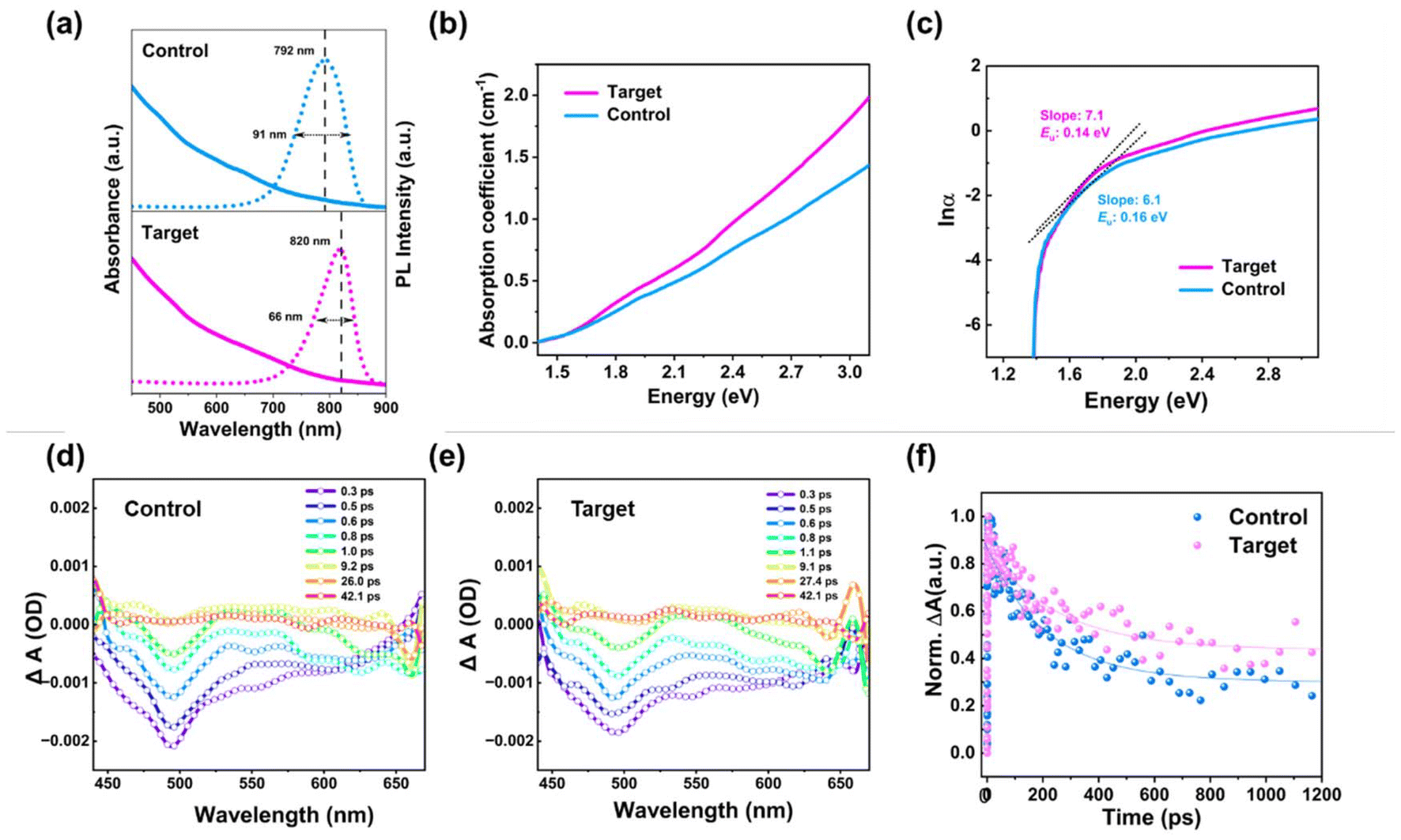 | ||
| Fig. 2 (a) The extracted UV-vis and PL emission of the final control and target CdSeTe QDs. (b) Absorption coefficient (α) and (c) plot of lnα vs. energy used to extract the Urbach energy of the target and control CdSeTe QD films. Ultrafast time-resolved TA spectra of (d) the target and (e) control CdSeTe QDs in toluene. (f) Transient absorption kinetics of the target and control CdSeTe QDs under identical conditions. | ||
The corresponding Eg values of the control and target QDs were estimated by extrapolating the linear portion of the plot of (ahν)2vs. hν with the results shown in Fig. 3a, in which the x-axis intercept of an extrapolated line from the linear regime of the curve represented the Eg value. It is clear that the Eg value slightly reduced from 1.84 eV to 1.78 eV after introducing the BF additive. Ultraviolet photoelectron spectroscopy (UPS) characterization was used to reveal the conduction band (CB) and valence band (VB) edge positions of typical control and target CdSeTe QDs with results shown in Fig. 3b and Table S1.† The ionization potentials (equivalent to the VB energy level) of control and target CdSeTe QDs were calculated to be −5.29 and −5.41 eV, respectively, by subtracting the excitation energy (21.22 eV) from the width of UPS images. The CB energy level is thus estimated to be at −3.45 and −3.63 eV. The higher CB level of the target CdSeTe QDs is due to the composition change of the elemental ratio, as discussed above. The schematic diagrams of the corresponding energy level distribution are presented in Fig. 3c. The suitable CB level of TiO2 of the control QDs promotes the driving force for electron injection from QDs into TiO2, consequently improving the electron injection rate and photovoltaic performance. A series of transient measurements were performed to investigate further the influence of fluorination treatment on the photogenerated carrier dynamics of QDs. The transient PL decay curves for the control and target QDs are displayed in Fig. 3d, revealing a reduced average PL lifetime from 12.68 to 9.89 ns. Both the PL quenching and shortened PL lifetime of the QD films with in situ fluorination treatment demonstrate the photoexcited electron transfer from QDs to the TiO2 electron transparent layer. The time of flight (TOF) method was also used to measure carrier mobility.26,27 A pulse laser of 375 nm was irradiated on the device, and the transit times under different biases were measured with an oscilloscope (Fig. 3e and f). The estimated transit time is proportional to the reciprocal of the applied bias, and the carrier mobility can be calculated from the slope divided by the thickness square. The carrier mobility of the target CdSeTe QDs is much higher than that of the control one.28 Therefore, as shown in Fig. 3g and h, in situ fluorination treatment effectively removes the oxide and dangling bond defects of CdSeTe QDs, further hinders the charge recombination, and accelerates the charge transport process.
 | ||
| Fig. 3 (a) Tauc plots of (αhν)2 as a function of the photon energy (hν), (b) high and low binding energy cut-off, (c) the resulting energy level of the target and control CdSeTe QDs with and without in situ fluorination treatment, (d) Tr-PL spectra of the control and target CdSeTe QD deposition on the TiO2 electrodes, (e and f) time-of-flight measurements of TiO2/QDs/Ag devices. (g and h) Schematic illustration of the trap state distribution and carrier localization for the control and target QD films and the corresponding charge transfer process diagram. | ||
To investigate the influence of the in situ fluorination treatment of CdSeTe QDs towards the carrier extraction and transfer process, we continued to construct self-powered photodetectors with a device configuration of ITO/TiO2/CdSeTe QDs/PF2/Ag (Fig. 4a). The detailed fabrication of the self-powered photodetectors are demonstrated in the ESI.† The cross-sectional scanning electron microscopy (SEM) image of the QD-based photodetector device is shown in Fig. S4a;† the thickness of the TiO2/QD active layer is approximately 0.4 nm. Here, the polymer 2-(4-[(3S,5S)-5-[(3,3-difluoropyrrolidin-1-yl)carbonyl]pyrrolidin-3-yl]piperazin-1-yl)pyrimidine (PF2) was first selected as the hole transport material. The energy level of the PF2 polymer is well-matchable with CdSeTe QDs. Meanwhile, as previously reported, the PF2 can form a much more uniform and smooth film than other hole-transport materials, reducing the interface charge recombination and accelerating the charge transfer.29Fig. 4b shows the corresponding band energy level diagram of the photodetector and proposed charge transfer pathways. Under illumination conditions, the excitons generated from the CdSeTe QD absorbers then diffuse to the interface between the donor and acceptor, where they can dissociate into free charge carriers, followed by the charge carriers diffusing to appropriate electrodes through the charge transfer layers under the built-in electric field.30 Therefore, the photodetector device can effectively operate without an external bias and realizes the self-powered operation mode. The molecular structure of PF2 is also shown in Fig. 4b. The current–voltage (I–V) measurements of the as-fabricated control and target CdSeTe QD devices under standard sunlight irradiation were performed and the results are shown in Fig. 4c. It is found that a certain photocurrent can be generated at an applied bias of 0 V, suggesting the unique self-powered capability of these photodetectors.31 The target CdSeTe QD photodetectors exhibited higher photocurrent densities and lower dark-current densities than the control device at 0 V bias. These results can be attributed to the higher concentration of photogenerated carriers and lower trap density, thus resulting in more efficient charge transport in the target CdSeTe QDs. This further reinforces the conclusion that the in situ fluorination treatment of the target QDs is a more effective photoinduced charge dynamic process than the control one, benefiting from the removal of the whole-body defects. The time-dependent photocurrent of the photodetectors was measured at a 0 V bias under standard sunlight illumination (Fig. 4d). The target CdSeTe QD-based photodetector exhibited two orders of magnitude higher photocurrent density compared with the control devices (0.21 mA cm−2vs. 0.11 mA cm−2). The on–off responsibility of the target photodetectors at 0 V bias was three orders higher than that of the control one. Moreover, as depicted in Fig. 4e, the external quantum efficiency (EQE) spectra of the target CdSeTe QD-based photodetectors are nearly twice those of the control device. The photodetectors exhibited a broad visible spectral photoresponse range, consistent with the wide absorption spectra of CdSeTe QDs. The photocurrent responsivities (R) and detectivity (D*) of the control and target photodetectors under different wavelengths are demonstrated in Fig. 4f. Since R is proportional to the EQE value, the target photodetector displayed a higher R value with a peak value of 280 mA W−1 at 510 nm. The specific D* value can also be calculated according to the equation  , where q is the electron charge, and Idark is the dark current, which is considered as the major noise in the detector.32S is the effective area of the detector, and R is the photoresponsivity at the corresponding wavelength. The D* of the target photodetector is remarkably higher than that of the control device. Table S2† presents a comparative analysis of the photoelectrical response performance of Cd-based photodetectors as reported in the literature. In addition, the time-dependent photocurrent of the photodetectors with the target and control CdSeTe QDs at 0 V bias was studied under single wavelength 606 nm laser illumination with three different light intensities (Fig. 4g and h). As the laser light intensity increased from 24.6 to 60.8 mW cm−2, the photocurrent of the control and target CdSeTe QD-based photodetectors significantly increased. However, the on–off responsibility ratio of the target QD-based photodetectors was much higher than that of the control one under all three light intensities. The high sensitivity under a negative bias indicates the increase of photoexcited carriers, which leads to the monotonic increase in the photocurrent at higher light intensity. We continued to measure the stability of the photodetector during continuous operation under standard sunlight illumination. As shown in Fig. S5a,† the change trends of Jsc in the CdSeTe QD-based photodetector with in situ fluorination treatment exhibit a relatively sluggish behavior, in contrast to that of the control device, which demonstrates a comparably quick degradation. This disparity is attributed to the CdSeTe QDs under in situ fluorination treatment to expedite charge extraction and mitigate charge recombination, ultimately enhancing the stability of the device. These results highlight the promising potential of the target QDs with enhanced charge transfer rates for optoelectronic applications. This high response ability at single visible wavelengths gives the photodetectors good potential for further optical communication and other optoelectronic applications.33
 | ||
| Fig. 4 (a) Schematic structure of the self-powered broadband photodetector, (b) energy band diagram and the selected polymer hole transport materials of the photodetector. The molecular structure of the PF2 hole-transport materials. (c) Current–voltage (I–V) curves of the control and target CdSeTe QD-based photodetectors in the dark and under standard sunlight (1 sun, 100 mW cm−2) illumination conditions. (d) Time-dependent photocurrent curves (I–t) of photodetectors of the control and target CdSeTe QD photodetectors under the standard sunlight at 0 V bias. (e) EQE spectra of CdSeTe QD photodetectors. (f) Responsivity (R) and specific detectivity (D*) spectra of the control and target CdSeTe QD photodetectors as a function of the incident light wavelength. Time-dependent photocurrent curves of the control (g) and the target (h) CdSeTe QD photodetectors under a 606 nm laser with different illumination power densities at 0 V bias. | ||
In addition, we continued to fabricate the CdSeTe QD-sensitized solar cells to validate the influence of in situ fluorination treatment further. The device structure of the high-efficiency QD-sensitized solar cell is shown in Fig. 5a. The immobilizing MPA-capped water-soluble CdSeTe QDs were obtained via the ligand-exchange process and then deposited on TiO2 film electrodes via the capping ligand-induced self-assembly approach.11,34,35 The cross-section SEM images of the QD-sensitized TiO2 photoanode utilized in solar cells, presented in Fig. S4b,† demonstrate a thickness of 10.3 μm. The J–V characteristics of the solar cells are plotted in Fig. 5b. The control CdSeTe QD-based devices produce a power conversion efficiency (PCE) of 11.12%, with photovoltaic parameters of a Voc of 0.794 V, a Jsc of 20.53 mA cm−2, and a fill factor (FF) of 0.682. Encouragingly, the target CdSeTe QD-based devices obtained a PCE of 12.79%, which resulted from the simultaneously enhanced PV parameters with a Voc of 0.869 V, a Jsc of 20.97 mA cm−2, and an FF of 0.702. Table S3† presents a comparative analysis of the photovoltaic performance of CdSeTe QD-sensitized solar cells as reported in recent literature. The results indicate that our device exhibits a higher Voc and PCE than those reported before. The enhanced photovoltaic parameters, especially Voc, of the target QD-based devices are ascribed to the suppressed charge recombination, which results from the improved charge extraction and increased charge recombination of the QDs with in situ fluorination treatment. The external quantum efficiency (EQE) spectra and integrated Jsc presented in Fig. 5c confirm the creation of a more significant photocurrent in the target QD devices. The integrated Jsc value of the champion solar cell with the target QDs is 19.54 mA cm−2, while that of the control QD-based device is 17.68 mA cm−2, similar to that obtained from the J–V curves. Electrochemical impedance spectroscopy (EIS) measurements were performed to explore the recombination kinetics behavior of solar cells and understand the increase in performance better.36 The value of charge recombination resistance (Rrec) is directly connected to the charge recombination process, and a bigger Rrec signifies a slower charge recombination rate. As demonstrated in Fig. 5d, the Rrec value of the samples with the target QDs is much higher than that of the control sample under different voltage biases. It can be shown that the recombination impedance of the device with the target CdSeTe QDs is substantially greater than that of the control CdSeTe QD-based devices, indicating that in situ fluorination treatment may effectively suppress charge recombination and accelerate charge extraction.37 The Nyquist charts for several passivation procedures at a forward bias of −0.80 V are shown in Fig. 5e, and the fitting parameters are presented in Table S4.† It can be found that the extracted Rrec value of the target QD-based solar cells (6.9 Ω cm2) is higher than that of the control QD-based cells (5.1 Ω cm2). The notably higher Rrec implies that the charge recombination rate of the target QD-based device is significantly suppressed. The suppressed recombination will enhance photovoltaic performance, especially for Voc. Furthermore, to explore the influence of different passivation processes on the dynamics of photo-generated electrons, the open-circuit voltage decay (OCVD) was measured.36 The Voc transient attenuation of the solar cell was recorded after the light was turned off. Fig. 5f shows the decay curves of the solar cells. The devices with the target CdSeTe QDs show a much slower Voc decay rate compared with the sample with the control CdSeTe QDs.37 Fig. S5b† displays the time-dependent PCE curve for a CdSeTe-based solar cell. Upon exposure to continuous standard sunlight for 200 min, the CdSeTe QD-based solar cells subjected to in situ fluorination retain 80% of their initial PCE. In contrast, the control device demonstrates a significant deterioration, maintaining only 68% of its initial intensity; therefore, the stability of solar cells retained with BF passivated CdSeTe QDs improved apparently. These results prove that the in situ fluorination treatment would harden the charge transport process by removing and passing whole-body defects toward chalcogenide QDs.
 | ||
| Fig. 5 (a) Schematic illustration of the QD-based solar cell. (b) J–V curves, (c) corresponding EQE spectra, and integrated Jsc of the champion solar cells with control and target CdSeTe QD-based solar cells under the standard conditions (AM 1.5 G, 100 mW cm−2). The corresponding (d) recombination resistance (Rrec) on the applied bias and (e) Nyquist curves under a bias voltage of 0.80 V recovered from the EIS measurement of solar cells under dark conditions. (f) The open-circuit voltage decay curves of the control and target CdSeTe QD-based solar cells. | ||
Conclusion
In summary, we have developed a simple and efficient in situ fluorination treatment to passivate the surface defects and thus enhance the charge transport process of the alloyed chalcogenide QDs. The BF molecule additive can decompose and release the F− ions to remove oxide traps and dangling bonds of the whole-body nanocrystals and improve the stability of QDs. As a result, the fabricated self-powered photodetector devices demonstrated high photocurrent density, two orders of magnitude higher than those of the control ones. The responsivity and specific detectivity of the target self-powered photodetectors reached up to 280 mA W−1 and 108 Jones under illumination with a broad spectral range to near-infrared region, respectively. Furthermore, the target QD-based sensitized solar cells have improved PCE with three simultaneously enhanced photovoltaic parameters. This study provided a facile method to achieve the removal and passivation of defects under the in situ and real-time states to promote the charge transport process for QD-related optoelectronic technologies.Data availability
All data required to understand the conclusions in the paper are presented in the main text and ESI.† Additional data related to this paper are available from the corresponding author upon request.Conflicts of interest
The authors declare that they have no conflict of interest.Acknowledgements
Z. Du is grateful for the financial support from the National Natural Science Foundation of China (Grant 51802169), the Natural Science Foundation of Shandong Province (Grant ZR2022MB068), the China Postdoctoral Science Foundation Funded Project (Grant 2018M632614), and the Applied Research Project for Postdoctoral Researchers in Qingdao. S. Huang is supported by the Jiangxi Province Critically Needed Overseas Talent Program (20232BCJ25039). J. Tang is supported by the State Key Project of International Cooperation Research (2017YFE0108300), the Program for Introducing Talents of Discipline to Universities (“111” Plan), and the Double Hundred Foreign Expert Project of Shandong Province.References
- F. P. García de Arquer, D. V. Talapin, V. I. Klimov, Y. Arakawa, M. Bayer and E. H. Sargent, Semiconductor quantum dots: Technological progress and future challenges, Science, 2021, 373(6555), eaaz8541 CrossRef PubMed.
- N. Zhou, H. Zhao, X. Li, P. Li, Y. You, M. Cai, L. Xia, H. Zhi, A. I. Channa, Z. M. Wang and X. Tong, Activating Earth-Abundant Element-Based Colloidal Copper Chalcogenide Quantum Dots for Photodetector and Optoelectronic Synapse Applications, ACS Mater. Lett., 2023, 5(4), 1209–1218 CrossRef CAS.
- Z. Li, J. Wei, F. Wang, Y. Tang, A. Li, Y. Guo, P. Huang, S. Brovelli, H. Shen and H. Li, Carrier Dynamics in Alloyed Chalcogenide Quantum Dots and Their Light–Emitting Devices, Adv. Energy Mater., 2021, 11(40), 2101693 CrossRef CAS.
- A.-Y. Zhu, R.-X. Ding, H.-T. Xu, C.-J. Tong and K. P. McKenna, Cu–Zn Cation Disorder in Kesterite Cu2ZnSn(SxSe1−x)4 Solar Cells, ACS Energy Lett., 2024, 9(2), 497–503 CrossRef CAS.
- M. Righetto, Y. Wang, K. A. Elmestekawy, C. Q. Xia, M. B. Johnston, G. Konstantatos and L. M. Herz, Cation-Disorder Engineering Promotes Efficient Charge-Carrier Transport in AgBiS(2) Nanocrystal Films, Adv. Mater., 2023, 35(48), e2305009 CrossRef PubMed.
- T. A. M. Fiducia, B. G. Mendis, K. Li, C. R. M. Grovenor, A. H. Munshi, K. Barth, W. S. Sampath, L. D. Wright, A. Abbas, J. W. Bowers and J. M. Walls, Understanding the role of selenium in defect passivation for highly efficient selenium-alloyed cadmium telluride solar cells, Nat. Energy, 2019, 4(6), 504–511 CrossRef CAS.
- J. D. Poplawsky, W. Guo, N. Paudel, A. Ng, K. More, D. Leonard and Y. Yan, Structural and compositional dependence of the CdTexSe1-x alloy layer photoactivity in CdTe-based solar cells, Nat. Commun., 2016, 7, 12537 CrossRef CAS PubMed.
- J. Xue, X. Yang, X. Bao, L. Fu, S. Li, M. Huang, J. Wang, H. Song, S. Chen, C. Chen, K. Li and J. Tang, Improved Carrier Lifetimes of CdSe Thin Film via Te Doping for Photovoltaic Application, ACS Appl. Mater. Interfaces, 2023, 15(14), 17858–17866 CrossRef CAS PubMed.
- S. Lal, M. Righetto, B. W. J. Putland, H. C. Sansom, S. G. Motti, H. Jin, M. B. Johnston, H. J. Snaith and L. M. Herz, The Role of Chemical Composition in Determining the Charge–Carrier Dynamics in (AgI)x(BiI3)y Rudorffites, Adv. Funct. Mater., 2024, 2315942 CrossRef CAS.
- H. Su, P. Lu, C. Zhu, W. Qiu, X. Qiu, K. Zhao, X. Lu, Y. Wei, X. Shi, L. Chen and F. Xu, Compositionally tailored order-disorder of cation-anion sublattices in Cu2Te1-S solid solution thermoelectric materials, Acta Mater., 2023, 248, 118764 CrossRef CAS.
- Z. Sun, Q. Hou, R. Zhang, J. Cheng, J. Kong, K. Wang, F. Liu, Z. Du and J. Tang, Facile surface pseudohalide pretreatment of quantum dots for efficient photovoltaics, Chem. Eng. J., 2023, 474, 145657 CrossRef CAS.
- Q. Zhang, M. He, Q. Wan, W. Zheng, M. Liu, C. Zhang, X. Liao, W. Zhan, L. Kong, X. Guo and L. Li, Suppressing thermal quenching of lead halide perovskite nanocrystals by constructing a wide-bandgap surface layer for achieving thermally stable white light-emitting diodes, Chem. Sci., 2022, 13(13), 3719–3727 RSC.
- Z. Wang, Y. Wei, Y. Chen, H. Zhang, D. Wang, J. Ke, Y. Liu and M. Hong, “Whole-Body” Fluorination for Highly Efficient and Ultra-Stable All-Inorganic Halide Perovskite Quantum Dots, Angew. Chem., Int. Ed., 2024, 63(8), e202315841 CrossRef CAS PubMed.
- M. Liu, Q. Wan, H. Wang, F. Carulli, X. Sun, W. Zheng, L. Kong, Q. Zhang, C. Zhang, Q. Zhang, S. Brovelli and L. Li, Suppression of temperature quenching in perovskite nanocrystals for efficient and thermally stable light-emitting diodes, Nat. Photonics, 2021, 15(5), 379–385 CrossRef CAS.
- Z. Sun, Q. Hou, J. Kong, K. Wang, R. Zhang, F. Liu, J. Ning, J. Tang and Z. Du, Surface Passivation toward Multiple Inherent Dangling Bonds in Indium Phosphide Quantum Dots, Inorg. Chem., 2024, 63(14), 6396–6407 CrossRef CAS PubMed.
- Q. Hou, Z. Du, Z. Sun, J. Kong, Y. Huang, K. Wang, J. Ning and J. Tang, Pseudohalogen Ammonium Salt-Assisted Syntheses of Large-Sized Indium Phosphide Quantum Dots with Near-Infrared Photoluminescence, J. Phys. Chem. Lett., 2024, 15(12), 3285–3293 CrossRef CAS PubMed.
- M. Imran, W. Paritmongkol, H. A. Mills, Y. Hassan, T. Zhu, Y.-K. Wang, Y. Liu, H. Wan, S. M. Park, E. Jung, J. Tam, Q. Lyu, G. F. Cotella, P. Ijaz, P. Chun and S. Hoogland, Molecular-Additive-Assisted Tellurium Homogenization in ZnSeTe Quantum Dots, Adv. Mater., 2023, 35(45), 2303528 CrossRef CAS PubMed.
- F. Yin, X. Zou, M. Chen, Z. Sun, X. Bao, Z. Du and J. Tang, Promoting the efficiency of quantum dots-based solar cells via the Cu:ZnSeS intermediate passivation layer, J. Mater. Res. Technol., 2022, 21, 1974–1983 CrossRef CAS.
- Y.-T. Huang, M. Schleuning, H. Hempel, Y. Zhang, M. Rusu, T. Unold, A. Musiienko, O. Karalis, N. Jung, S. J. Zelewski, A. J. Britton, N. Ngoh, W. Song, L. C. Hirst, H. Sirringhaus, S. D. Stranks, A. Rao, I. Levine and R. L. Z. Hoye, Elucidating the Role of Ligand Engineering on Local and Macroscopic Charge-Carrier Transport in NaBiS2 Nanocrystal Thin Films, Adv. Funct. Mater., 2024, 34(29), 2310283 CrossRef CAS.
- A. S. Portniagin, A. A. Sergeev, K. A. Sergeeva, S. Wang, Z. Li, J. Ning, C. C. S. Chan, S. V. Kershaw, X. Zhong, K. S. Wong and A. L. Rogach, Removing Cadmium Impurities from Cation-Exchange-Derived CuInSe2/CuInS2 Nanorods for Enhanced Infrared Emission and Photodetection, Adv. Funct. Mater., 2024, 2400942 CrossRef CAS.
- R. Tenne, S. Pedetti, M. Kazes, S. Ithurria, L. Houben, B. Nadal, D. Oron and B. Dubertret, From dilute isovalent substitution to alloying in CdSeTe nanoplatelets, Phys. Chem. Chem. Phys., 2016, 18(22), 15295–15303 RSC.
- J. Park, A. Jayaraman, A. W. Schrader, G. W. Hwang and H.-S. Han, Controllable modulation of precursor reactivity using chemical additives for systematic synthesis of high-quality quantum dots, Nat. Commun., 2020, 11(1), 5748 CrossRef CAS PubMed.
- J. Xue, X. Yang, X. Bao, L. Fu, S. Li, M. Huang, J. Wang, H. Song, S. Chen, C. Chen, K. Li and J. Tang, Improved Carrier Lifetimes of CdSe Thin Film via Te Doping for Photovoltaic Application, ACS Appl. Mater. Interfaces, 2023, 15(14), 17858–17866 CrossRef CAS PubMed.
- N. K. Tailor and S. Satapathi, Structural Disorder and Spin Dynamics Study in Millimeter-Sized All-Inorganic Lead-Free Cesium Bismuth Halide Perovskite Single Crystals, ACS Appl. Energy Mater., 2020, 3(12), 11732–11740 CrossRef CAS.
- Q. Xiao, Y. Zhao, Z. Huang, Y. Liu, P. Chen, S. Wang, S. Zhang, Y. Zhang and Y. Song, Benzoyl Sulfonyl Molecules for Bilateral Passivation and Crystalline Regulation at Buried Interfaces toward High-Performance Perovskite Solar Cells, Adv. Funct. Mater., 2024, 34(22), 2314472 CrossRef CAS.
- C. Liu, S. Wu, Y. Gao, Y. Feng, X. Wang, Y. Xie, J. Zheng, H. Zhu, Z. Li, R. E. I. Schropp, K. Shen and Y. Mai, Band Gap and Defect Engineering for High-Performance Cadmium-free Sb2(S,Se)3 Solar Cells and Modules, Adv. Funct. Mater., 2022, 32(49), 2209601 CrossRef CAS.
- Y. Liu, X. Zheng, Y. Fang, Y. Zhou, Z. Ni, X. Xiao, S. Chen and J. Huang, Ligand assisted growth of perovskite single crystals with low defect density, Nat. Commun., 2021, 12(1), 1686 CrossRef CAS PubMed.
- W.-G. Li, X.-D. Wang, Y.-H. Huang and D.-B. Kuang, Ultrasound-Assisted Crystallization Enables Large-Area Perovskite Quasi-Monocrystalline Film for High-Sensitive X-ray Detection and Imaging, Adv. Mater., 2023, 35(31), 2210878 CrossRef CAS PubMed.
- X. Ma, Q. An, O. A. Ibraikulov, P. Lévêque, T. Heiser, N. Leclerc, X. Zhang and F. Zhang, Efficient ternary organic photovoltaics with two polymer donors by minimizing energy loss, J. Mater. Chem. A, 2020, 8(3), 1265–1272 RSC.
- S. Li, J. H. Jang, W. Chung, H. Seung, S. I. Park, H. Ma, W. J. Pyo, C. Choi, D. S. Chung, D.-H. Kim, M. K. Choi and J. Yang, Ultrathin Self-Powered Heavy-Metal-Free Cu–In–Se Quantum Dot Photodetectors for Wearable Health Monitoring, ACS Nano, 2023, 17(20), 20013–20023 CrossRef CAS PubMed.
- T. Shen, B. Li, K. Zheng, T. Pullerits, G. Cao and J. Tian, Surface Engineering of Quantum Dots for Remarkably High Detectivity Photodetectors, J. Phys. Chem. Lett., 2018, 9(12), 3285–3294 CrossRef CAS PubMed.
- M. Peng, Y. Tao, D. Bao, K. Wang and X. Sun, Rational synthesis of core/shell heterostructured quantum dots for improved self-powered photodetection performance enabled by energy band engineering, Nano Energy, 2024, 129, 110033 CrossRef CAS.
- B. Chen, J. Xu, S. Shi, L. Kong, X. Zhang and L. Li, UV–Vis–NIR Broadband Self-Powered CuInS2/SnO2 Photodetectors and the Application in Encrypted Optical Communication, ACS Appl. Mater. Interfaces, 2024, 16(22), 28917–28927 CrossRef CAS PubMed.
- J. Du, Z. Du, J.-S. Hu, Z. Pan, Q. Shen, J. Sun, D. Long, H. Dong, L. Sun, X. Zhong and L.-J. Wan, Zn–Cu–In–Se Quantum Dot Solar Cells with a Certified Power Conversion Efficiency of 11.6%, J. Am. Chem. Soc., 2016, 138(12), 4201–4209 CrossRef CAS PubMed.
- Z. Du, Z. Pan, F. Fabregat-Santiago, K. Zhao, D. Long, H. Zhang, Y. Zhao, X. Zhong, J.-S. Yu and J. Bisquert, Carbon Counter-Electrode-Based Quantum-Dot-Sensitized Solar Cells with Certified Efficiency Exceeding 11%, J. Phys. Chem. Lett., 2016, 7(16), 3103–3111 CrossRef CAS PubMed.
- Z. Zhang, H. Song, W. Wang, H. Rao, Y. Fang, Z. Pan and X. Zhong, Dual Ligand Capped Quantum Dots Improving Loading Amount for High-Efficiency Quantum Dot-Sensitized Solar Cells, ACS Energy Lett., 2023, 8(1), 647–656 CrossRef CAS.
- H. Song, Y. Lin, Z. Zhang, H. Rao, W. Wang, Y. Fang, Z. Pan and X. Zhong, Improving the Efficiency of Quantum Dot Sensitized Solar Cells beyond 15% via Secondary Deposition, J. Am. Chem. Soc., 2021, 143(12), 4790–4800 CrossRef CAS PubMed.
Footnotes |
| † Electronic supplementary information (ESI) available: Experimental section, SEM, UV-Vis spectra, XPS spectra, device stability, and band edge level. See DOI: https://doi.org/10.1039/d4nr04410j |
| ‡ These authors contributed equally. |
| This journal is © The Royal Society of Chemistry 2025 |