DOI:
10.1039/D4NR04894F
(Paper)
Nanoscale, 2025,
17, 4732-4739
A linearly polarized AC-driven perovskite light emitting device with nanoscale metal contact†
Received
21st November 2024
, Accepted 14th January 2025
First published on 15th January 2025
Abstract
Electroluminescent (EL) devices consisting of a single metal–semiconductor contact and a gate effect structure have garnered significant attention in the field of perovskite light-emitting devices. This interest is largely due to the thermal stability of the active layer and the simplicity of the device structure. However, the application of these devices in large-area light-emitting applications is hindered by the inherently low carrier mobility in perovskite materials. In our study, we addressed this limitation by optimizing the nanostructure within the electrodes, which resulted in enhanced electroluminescence and linear polarization. To confirm the luminescence mechanism and the observed enhancement, we conducted comprehensive electrical and optical characterization studies. These characterization studies demonstrated the effectiveness of our approach in improving the performance of perovskite-based EL devices, paving the way for their broader application in large-area light-emitting technologies.
Introduction
Perovskite materials have attracted substantial interest in light-emitting devices1,2 and display applications3 due to their exceptional tunability, long carrier lifetime, extended carrier diffusion length, and high photoluminescence quantum yield (PLQY).4,5 Their ease of synthesis and thin-film processing techniques further bolster their appeal in the field of optoelectronics, alongside their low cost, which enhances their commercial viability. However, despite their remarkable optical properties, perovskite materials face significant challenges in commercialization. These challenges include low carrier injection efficiency and poor thermal stability. The low carrier injection efficiency necessitates precise band alignment within devices.6–8 Additionally, even after addressing injection issues, the devices tend to degrade rapidly due to thermal effects resulting from carrier interactions, requiring a careful balance between these factors.
For materials with low environmental stability, alternating current (AC) light-emitting devices present a viable solution. The use of AC significantly reduces thermal damage as it prevents substantial charge accumulation within the material.9–13 Additionally, the simple structure of AC light-emitting devices allows for the deposition of the light-emitting active layer on top after completing the device structure, minimizing the risk of process-induced material damage. Furthermore, the light-emission mechanism in AC devices is less dependent on the Schottky barrier at the metal–material interface, effectively mitigating the issue of insufficient carrier injection. Previous studies have demonstrated the potential of AC transient light-emitting devices with these materials. Lien et al. achieved stable large-area emission,14–16 while Klein et al. utilized a field-effect transistor structure and a multi-electrode configuration to fabricate perovskite transient light-emitting devices. By integrating FIB-patterned perovskites, they achieved highly directional polarized light emission, with the effect being highly adjustable based on the grating period.17–19 However, the low carrier mobility of perovskites necessitates operation at low temperatures and high voltages to achieve optimal performance. This requirement poses a challenge for scalability and limits the development of these devices for the consumer electronics market.
Inspired by these studies, we have fabricated a unipolar-controlled perovskite transient light-emitting device. In the design of this device, we integrated nanoscale metal electrodes with the transient light-emitting structure, leveraging the advanced nanofabrication techniques available for metal structures. These techniques are known for their effectiveness in enhancing optical gain and regulating the electric field;20–23 this integration resulted in stable large-area perovskite emission at room temperature and low voltage. Furthermore, since the perovskite thin film is deposited after the completion of device fabrication, it avoids any damage to the material from post-processing steps. This approach underscores the significant potential of patterned electrode designs in developing perovskite light-emitting devices.
Results and discussion
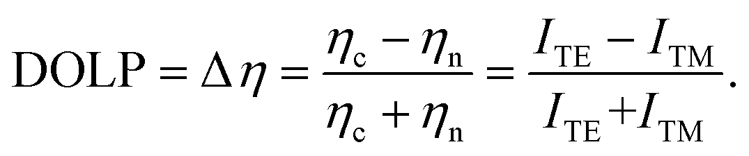
Fig. 1(a) and (b) illustrate the schematic diagram and structural parameters of the transient perovskite light-emitting device, respectively. Beneath the perovskite film, a hollow silver square electrode with a line width of 100 μm was fabricated to serve as the electrode. A 5 nm Al2O3 protective layer was then deposited on the electrodes before completing the preparation of the MAPbI3 film on the device sample. Fig. 1(c) and (d) present the extinction, photoluminescence (PL), and X-ray diffraction (XRD) spectra of the MAPbI3 film. The PL and extinction spectra were obtained using a 355 nm pulsed laser and white light, respectively. The extinction peak is located at 751 nm, while the PL peak is at 767 nm. The XRD spectrum exhibits sharp diffraction peaks at 14.11°, 28.39°, and 31.83°, corresponding to the (110), (220), and (222) crystal planes, respectively, which are consistent with previously reported MAPbI3 structures.24 In the absence of nanostructures within the electrodes, polarized PL measurements, shown in Fig. 1(e), confirmed that MAPbI3 did not exhibit significant polarization tendencies at various polarization angles.
 |
| | Fig. 1 (a) Schematic 3D structure for the transient perovskite light-emitting device. (b) Cross-sectional view of the device. (c) Extinction and PL spectra for MAPbI3. (d) X-ray diffraction spectrum for MAPbI3. (e) PL intensity for MAPbI3 at different polarization degrees. | |
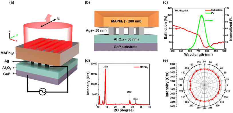
The measurements taken after device illumination are depicted in Fig. 2. It should be noted that the device here does not contain silver nanogratings, but only hollow silver electrodes. Fig. 2(a) shows the configuration of the illuminated perovskite device observed under an optical microscope and a near-infrared electron-multiplying charged-coupled device (NIR-EMCCD). It was confirmed that the perovskite emits light along the interface with the electrode as seen through the EMCCD. To investigate the influence of electrode shape and size on emission, electrodes of various shapes and hollow sizes were designed (ESI Fig. S1†). In the case of circular electrodes, light emission persisted along the interface between the perovskite and the hollow part of the electrode, consistent with the results shown in Fig. 2(a). However, the changes in the size and shape of the electrodes did not influence the emission a lot; MAPbI3 only emits light along the inner edges of the electrodes, with the emission area being approximately 1.5–1.7 μm in length. This phenomenon is related to the mechanism of the device. First, the AC-driven emission mechanism primarily relies on the oscillation of the electric field, where charges mainly oscillate between the silver electrode and the substrate, resulting in recombination luminescence. In other words, the strength of the electric field determines the probability of recombination luminescence. Consequently, the interface between the electrode and the substrate has a higher recombination probability because this region has the strongest electric field. In contrast, the central region of the hollow electrode is the farthest from the electrode and thus emits almost no light, as shown in Fig. S1(a),† where the yellow line represents the electric field, and the red and blue spheres represent opposite charges. Fig. S1(b)† shows an actual EMCCD image, where d denotes the inner diameter of the hollow electrode. In the normalized spectra shown in Fig. 2(b), a comparison between PL and electroluminescence (EL) data reveals a redshift in the EL peak relative to the PL peak. This redshift indicates a higher probability of recombination near the gate and electrode during electrical excitation. Consequently, the EL signal primarily originates from the contact–perovskite interface and undergoes radiative recombination after traversing the surface film. Additionally, apart from the influence of the material's high refractive index, photon recycling during propagation within the film also contributes to the observed redshift in the peak.17,25
 |
| | Fig. 2 (a) Optical image of the device and the emission image taken using an NIR-EMCCD. (b) PL and EL spectra of the perovskite light-emitting device showing a redshift of the EL peak. (c) Frequency dependent EL intensity of the device as a function of applied voltage. (d) Thermionic emission EL characteristics. (e) Tunneling recombination EL characteristics. (f) Schematic of the working mechanism of the AC-driven perovskite EL device. | |
Subsequently, we analyzed the frequency dependence of the EL signal as a function of applied voltage, as depicted in Fig. 2(c). It should be noted that the voltage in this article's data is defined as the voltage difference between two peaks (Vpp). The EL signal exhibits a significant enhancement at voltages exceeding 12 V. Under varying frequency conditions, it was observed that the EL signal markedly increases when the frequency surpasses 200 kHz. This phenomenon occurs because, at lower frequencies, carrier activity in the perovskite is limited, necessitating a higher oscillation frequency to enhance the probability of radiative recombination. When the frequency is sufficiently high (>200 kHz), the intercept of the region with the highest slope on the voltage axis, defined as the turn-on voltage, is approximately 12 V. To confirm the light-emission mechanism of the device, we employed the model of EL intensity versus voltage, as proposed in recent studies on AC light-emitting devices. The relationship is described by the following equation:26,27
where
α is a constant related to excitons in semiconductor materials and
κ represents the injection concentration of carriers. This characteristic is evident in the data at 500 kHz and 800 kHz in
Fig. 2(c), in the high-voltage region, consistent with the proposed model. According to previous studies, AC semiconductor light-emitting devices are primarily governed by two mechanisms: thermionic emission and carrier tunneling recombination.
28–34 While thermionic emission is frequently referenced in perovskite light-emitting devices, carrier tunneling effects are less discussed. This is likely because perovskites are more commonly utilized in DC devices, such as LEDs and batteries. Therefore, we will further explore these two emission mechanisms in this context.
Thermionic emission typically occurs under high-temperature conditions and can be characterized as a function of current density and temperature. In the presence of an AC electric field and constant temperature, voltage must be introduced. Consequently, the Schottky equation can be simplified to a function of voltage as follows:
| | I(V) = ISE![[thin space (1/6-em)]](https://www.rsc.org/images/entities/char_2009.gif) exp(A√V) exp(A√V) | (2) |
where
ISE is the intensity of spontaneous emission and
A is the Richardson coefficient. Thus, if the process follows thermionic emission, the natural logarithm of the EL intensity should be directly proportional to the square root of the voltage. As shown in
Fig. 2(d), the natural logarithm of the EL intensity exhibits a proportional relationship with the square root of the voltage when the voltage is below 12 V, with the slope remaining relatively constant. This indicates that below the threshold voltage, the device's emission is predominantly due to thermionic emission.
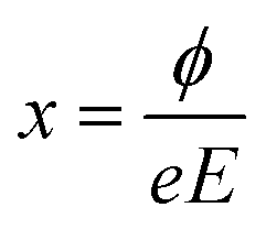
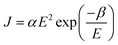
Conversely, tunneling effects are influenced by the height of the Schottky barrier, with the barrier width characterized by the following equation:
| |  | (3) |
where
ϕ represents the barrier height and
E denotes the external electric field strength. Therefore, it can be inferred that an increase in electric field strength results in a reduction in barrier width, thereby enhancing the likelihood of tunneling effects
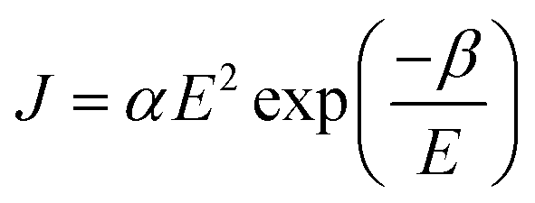
35. The tunneling effect can be described by the following equation:
| |  | (4) |
where
J represents the induced current and
α and
β are constants. After simplification, we obtain:
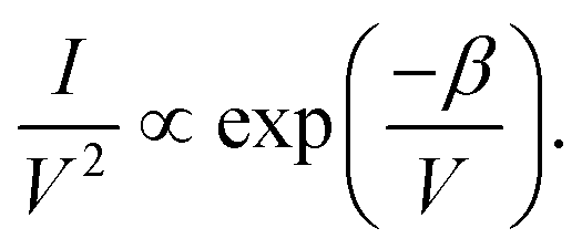
| |  | (5) |
This equation demonstrates that when the tunneling effect predominates in the device, ln(I/V2) exhibits a negative linear relationship with 1/V. As illustrated in Fig. 2(e), it is notable that the intercept of this negative linear relationship with 1/V approximately corresponds to the turn-on voltage. These findings imply that the operating principle of the transient perovskite light-emitting device aligns with the classic AC semiconductor light-emitting model.36 Based on the above discussion, the AC-driven electroluminescence (EL) mechanism of the perovskite is illustrated in Fig. 2(f). In this figure, a steady negative bias is applied to the substrate, which serves as the device's gate electrode, during the period marked as 1. During this phase, holes accumulate at the bottom of the MAPbI3 film, while the Schottky barrier prevents carrier flow from the perovskite to the gate. At the next moment, labeled as 2, the bias shifts from negative to positive, leading to the capacitive element between the top electrode and the gate inducing a potential difference. This sudden potential drop results in conduction band bending, facilitating the recombination of the injected electrons with the holes generated in the moment labeled as 1, ultimately leading to photon emission.
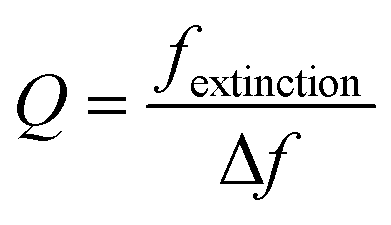
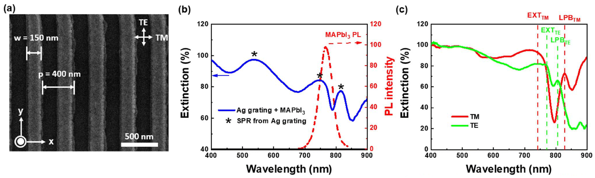
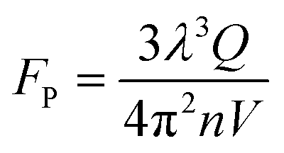
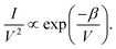
Next, we fabricated gratings within the electrodes to investigate the gain and operating mechanism of the patterned electrodes. Initially, we utilized scanning electron microscopy (SEM) to examine the surface morphology, with the structural parameters depicted in Fig. 3(a); for the MAPbI3 growing conditions in the grating, please check Fig. S3(a).† We define the direction perpendicular to the grating as the transverse magnetic (TM) direction, a convention that will be maintained in all subsequent measurements. In Fig. 3(b), we obtained the extinction spectra of the sample to determine the quality factor (Q) of the structure. The quality factor is defined as:
| |  | (6) |
where
fextinction is the frequency of the extinction peak and Δ
f is the full width at half maximum (FWHM) of the extinction peak in the frequency domain. For MAPbI
3 combined with a silver grating, distinct metal peaks appear in the high absorption region of the perovskite. This phenomenon is attributed to the extinction peak caused by surface plasmon polaritons (SPPs) generated when the high-refractive index MAPbI
3 (
nMAPbI3 ≃ 2.6) covers the surface of the silver grating and aligns with the exciton and emission peaks (PL) of MAPbI
3. This alignment signifies a strong exciton–polariton effect and enhanced emission within this wavelength range.
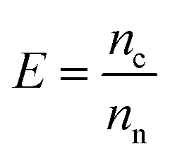
37–45 To predict the coupling strength of TE/TM polarizations, we recorded the absorption spectrum of MAPbI
3 with silver grating structures for both TE and TM polarizations, highlighting their contrasts, as depicted in
Fig. 3(c). EXT
TE and EXT
TM denote the extinction peaks near the exciton for transverse electric (TE) and transverse magnetic (TM) polarizations, respectively. Similarly, LPB
TE and LPB
TM represent the lower energy polariton extinction peaks for TE and TM polarizations. The coupling strength, detuning (
δ), and Rabi splitting (
Ω) are derived from the following equations:
| | | δ = Eexciton − Ephoton | (7) |
where
Eexciton represents the energy of the exciton,
Ephoton represents the energy of the photon, and
δ represents the energy difference between the photon and the exciton at zero momentum. A smaller
δ indicates stronger coupling. In this device, the photons are emitted by MAPbI
3 at approximately 1.60 eV, with an energy difference of 1.6 meV for EXT
TE and 65.8 meV for EXT
TM, resulting in the smallest energy detuning in the TE direction. The magnitude of the Rabi splitting (
Ω) is used to determine the strength of the coupling.
EUPB and
ELPB represent the upper and lower polariton branches, respectively. Experimentally, the upper polariton branch (UPB) is often located in the high absorption region of the material and is not easily observed, whereas the lower polariton branch (LPB) is more readily observed. When the LPB is closest to the exciton peak, the energy exchange between the photon and the exciton is most intense. Consequently, we conclude that the coupling strength of photons in the TE direction is stronger than that in the TM direction.
 |
| | Fig. 3 (a) SEM image for the silver grating electrodes. (b) Extinction spectrum of the silver grating with MAPbI3 and the PL spectra of MAPbI3. (c) Extinction spectrum of the silver grating integrated with MAPbI3 in the TE and TM directions for the analysis of exciton–polariton interaction. | |
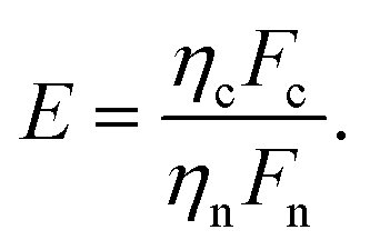
To further quantify the gain enhancement in metal–semiconductor systems, the Purcell factor (FP) serves as a crucial parameter. It characterizes the oscillation strength of an emitter within a resonant cavity. When the emission of photons aligns with the resonant mode of the cavity, FP can be expressed by the following equation:46
| |  | (9) |
where
λ is the wavelength of photon emission,
n is the refractive index of the emitting material, and
V is the volume of the resonant mode. The TE and TM electric field distribution map of the grating structure with the perovskite materials is shown in Fig. S2(a).
† The distribution reveals that the electric field predominantly oscillates within the MAPbI
3 thin film, which is attributed to its high refractive index.
47,48 Upon interaction with the metal, the electric field is confined within the high refractive index material. There has been a significant enhancement of the electric field when excited in the TE mode and it is primarily located at the top of the silver grating inside the MAPbI
3 film. Notably, in the absence of silver gratings, air gaps formed between the MAPbI
3 and Al
2O
3 due to the fabrication process, which typically yields large, dense perovskite crystals that do not infiltrate nanoscale gaps, as shown in Fig. S3(b).
† This phenomenon has been previously discussed in our earlier work.
49 Consequently, our simulation modelling accounts for this condition. The
Q factor calculation, illustrated in Fig. S2b,
† involved extracting the extinction peaks of the TE and TM modes
via curve fitting, resulting in a
Q value with an
FP of approximately 1.21.
To investigate the combination of the Purcell factor with the measured data, we referenced previous literature on laser resonant cavities.8,38,39,50–60 Initially, we defined the gain factor (E) as follows:
| |  | (10) |
where
nc represents the photon flux after passing through the resonant cavity and
nn represents the photon flux without any structure. When the integration time for the spontaneous emission is the same, the photon flux can be considered as the emission intensity:
In experiments, we obtain E by dividing the emission signal with the structure gain by the signal without gain. At this point, to introduce the Purcell factor, we generalize the emission intensity as follows:
where
η is the coupling efficiency and
Γ is the total decay rate of photons, and we substitute them into the equation as follows:
where
Γo is the total decay rate in free space and
F is the Purcell factor. Combining the definition of
E, we can obtain:
| |  | (14) |
To simplify the calculation, we set Fn to 1. By combining this with the results from Fig. S2b,† we obtain the efficiency ratio for the two polarization directions, ηc/ηn. This value allows us to determine the relative efficiency (Δη), which represents the degree of polarization as follows:
| |  | (15) |
To ascertain the impact of integrating gratings into the device, we performed electroluminescence (EL) measurements on the samples depicted in Fig. 3. Fig. 4(a) presents the emission of the device as observed under an optical microscope (OM) and a NIR-EMCCD. It is evident that the device with gratings exhibits a significantly enhanced emission area compared to the device without gratings (Fig. 2a). Using the findings from Fig. 2, we illustrated the emission mechanism after incorporating the gratings, as shown in Fig. 4(b). The MAPbI3 film deposits on the device surface, causing carriers to accumulate at the top of the silver grating under a constant voltage, while carriers of opposite nature are induced within the MAPbI3 film at the grating edges. Radiative recombination then occurs upon voltage reversal. Notably, the recombination emission location is proximal to the coupling position illustrated in Fig. S2a.† Therefore, when the structure's coupling band aligns with the emission wavelength of MAPbI3, the electric field in the transverse electric (TE) direction is enhanced, resulting in an amplified emission signal. The results of polarization-sensitive EL measurements are displayed in Fig. 4(c), indicating a gain in the TE direction for MAPbI3 EL. The degree of linear polarization (DOLP) calculated from EL results aligns with those derived after incorporating the Purcell factor, as shown in Fig. 4(d). To confirm that polarization enhancement primarily arises from optical coupling, we compared the DOLP results in EL with those in photoluminescence (PL), revealing similar trends. This consistency confirms the polarization enhancement mechanism within the device. It is noteworthy that the EL effect surpasses the PL effect, attributed to EL emission originating from the electrode–MAPbI3 interface, which is closer to the region of electric field enhancement, whereas the PL-excited region primarily originates from the MAPbI3–air interface, resulting in a less effective structural gain response.
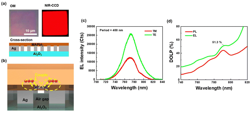 |
| | Fig. 4 (a) Optical image of the device with the grating structure and the emission image recorded using an NIR-EMCCD. (b) Emission and coupling mechanism in the perovskite device. (c) EL spectra of the device under TE and TM polarization. (d) DOLP extracted from the EL spectra of the device. | |
Conclusions
In this study, we engineered patterned electrode designs to fabricate perovskite electroluminescent devices that bypass the need for band alignment and exhibit tunable emission characteristics. By introducing nanostructures within the electrodes, the devices displayed significant linear polarization, consistent with extinction spectrum results. This confirms the feasibility of integrating electrodes with emission and validates the enhancement mechanism. Although the precise carrier dynamics within the device requires further elucidation, these findings suggest promising potential for highly efficient and stable perovskite electroluminescent devices, as well as applications in large-area emission.
Methods
Device fabrication
In the device fabrication, a GaP wafer was employed as the substrate. Initially, a 50 nm Al2O3 film was deposited on the surface using Atomic Layer Deposition (ALD) to function as the gate. Subsequently, A5 PMMA was applied via spin coating, with the process parameters set to 1000 rpm for 10 seconds and 3500 rpm for 120 seconds. Post-spin coating, the sample underwent annealing at 180 °C for 2 minutes. Electron beam lithography was utilized to expose the grating pattern onto the PMMA layer. Following the development of the pattern, a 50 nm silver film was deposited using electron beam evaporation with an E-gun, and the resist was lifted off to complete the grating fabrication. Next, DNR-L300 was spin-coated onto the fabricated grating, and a UV direct writer was employed to define the silver electrode pattern. Following the development process, an additional evaporation step was conducted to deposit the electrodes, followed by a lift-off process to finalize the patterned electrodes. The ground electrode was similarly defined using the UV direct writer. To ensure contact with the GaP, the Al2O3 layer was etched with BOE after development, preceding the electrode deposition process. Finally, a 5 nm Al2O3 film was deposited via ALD to serve as a protective layer between the device and the perovskite.
Fabrication of the perovskite precursor
Methylammonium iodide (MAI) and lead iodide (PbI2) were purchased separately from Greatcell Solar Materials and Sigma-Aldrich, respectively. These compounds were combined in a 1:1 molar ratio to achieve a concentration of 1 M. A solvent mixture of gamma-butyrolactone (GBL) and dimethyl sulfoxide (DMSO) in a 7:3 volume ratio was employed. The resulting mixture was stirred at 65 °C for 30 minutes to form the precursor solution. All procedures were conducted within a nitrogen glovebox environment.
Perovskite thin film fabrication
The patterned electrode substrate, after being exposed to UV-ozone for 30 minutes, was returned to the glovebox. The preparation of the perovskite precursor involved a spin-coating process with an initial spin at 1000 rpm for 10 seconds, followed by 5000 rpm for 50 seconds. To achieve a dense perovskite film, toluene was introduced as an antisolvent for 20 seconds into the spin-coating process. The device fabrication was completed by annealing the sample on a hot plate at 100 °C for 30 minutes.
Extinction spectrum measurement
We employed a custom-designed optical system integrated with an optical microscope to conduct spectral measurements. This optical configuration incorporates a rotatable linear polarizer, enabling measurements across various polarization directions.
NIR-EMCCD integrated PL and EL system
In photoluminescence (PL) measurements, a 450 nm continuous-wave laser with a power output below 5 μW is used as the excitation source. The laser beam is focused on a spot size of approximately 3 μm using a 100× objective lens. For electroluminescence (EL) measurements, an alternating current power supply with a voltage amplitude of 20 V, in conjunction with a probe holder, is utilized for device excitation. Both PL and EL signals are collected through the same objective lens and directed into a HORIBA IHR320 spectrometer for analysis. To ensure that the imaging is not affected by extraneous light, a filter is placed in front of the EMCCD to filter out light outside the 700–850 nm wavelength range.
High resolution X-ray diffraction and scanning electron microscopy
We employed the Bede D1 X-ray diffraction (XRD) system to perform scans under the conditions of 40 kV and 40 mA, acquiring diffractograms within the 2θ range of 10° to 40°. Additionally, we used the Hitachi SU-8010 scanning electron microscope (SEM) to examine the surface morphology of the samples, operating at an accelerating voltage of 10 kV.
Data availability
The data supporting this article have been included as part of the ESI.†
Conflicts of interest
There are no conflicts to declare.
Acknowledgements
This work is supported by research funding from Academia Sinica in Taiwan and the National Science Technology Council under Contract No. NSTC 113-2112-M-001-040, NSTC 113-2112-M-019-004, NSTC 110-2221-E-A49-089 -MY3 and NSTC 112-2112-M-001-074.
References
- Z. Wei and J. Xing, J. Phys. Chem. Lett., 2019, 10, 3035–3042 CrossRef CAS PubMed
 .
.
- Y. K. Wang, F. Yuan, Y. Dong, J. Y. Li, A. Johnston, B. Chen, M. I. Saidaminov, C. Zhou, X. Zheng and Y. Hou, Angew. Chem., Int. Ed., 2021, 60, 16164–16170 CrossRef CAS PubMed .
- Y.-C. Wang, H. Li, Y.-H. Hong, K.-B. Hong, F.-C. Chen, C.-H. Hsu, R.-K. Lee, C. Conti, T. S. Kao and T.-C. Lu, ACS Nano, 2019, 13, 5421–5429 CrossRef CAS PubMed .
- Y.-H. Kim, S. Kim, A. Kakekhani, J. Park, J. Park, Y.-H. Lee, H. Xu, S. Nagane, R. B. Wexler and D.-H. Kim, Nat. Photonics, 2021, 15, 148–155 CrossRef CAS .
- T. Wu, W. Pisula, M. Y. A. Rashid and P. Gao, Adv. Electron. Mater., 2019, 5, 1900444 CrossRef CAS .
- D. Yang, B. Zhao, T. Yang, R. Lai, D. Lan, R. H. Friend and D. Di, Adv. Funct. Mater., 2022, 32, 2109495 CrossRef CAS .
- J. Xu, D. L. Carroll, G. M. Smith, C. Dun and Y. Cui, Sci. Rep., 2016, 6, 24116 CrossRef CAS PubMed .
- M. A. Green, A. Ho-Baillie and H. J. Snaith, Nat. Photonics, 2014, 8, 506–514 CrossRef CAS .
- C. C. Tong and K. C. Hwang, J. Phys. Chem. C, 2007, 111, 3490–3494 CrossRef CAS .
- Q. Wang, J. Ding, D. Ma, Y. Cheng, L. Wang and F. Wang, Adv. Mater., 2009, 21, 2397–2401 CrossRef CAS .
- Z. Xiao, R. A. Kerner, L. Zhao, N. L. Tran, K. M. Lee, T.-W. Koh, G. D. Scholes and B. P. Rand, Nat. Photonics, 2017, 11, 108–115 CrossRef CAS .
- X. Xu, K. Xiao, G. Hou, Y. Zhang, T. Zhu, L. Xu, J. Xu and K. Chen, Adv. Opt. Mater., 2021, 9, 2100636 CrossRef CAS .
- S. Yu, J. Hu, H. Zhang, G. Zhao, B. Li, Y. Xia and Y. Chen, ACS Photonics, 2022, 9, 1852–1874 CrossRef CAS .
- V. Wood, M. J. Panzer, D. Bozyigit, Y. Shirasaki, I. Rousseau, S. Geyer, M. G. Bawendi and V. Bulovic, Nano Lett., 2011, 11, 2927–2932 CrossRef CAS PubMed .
- S. H. Cho, J. Sung, I. Hwang, R. H. Kim, Y. S. Choi, S. S. Jo, T. W. Lee and C. Park, Adv. Mater., 2012, 24, 4540–4546 CrossRef CAS PubMed .
- D.-H. Lien, M. Amani, S. B. Desai, G. H. Ahn, K. Han, J.-H. He, J. W. Ager III, M. C. Wu and A. Javey, Nat. Commun., 2018, 9, 1229 CrossRef PubMed .
- M. Klein, K. Blecharz, B. W. H. Cheng, A. Bruno and C. Soci, Adv. Electron. Mater., 2023, 9, 2300270 CrossRef CAS .
- M. Klein, Y. Wang, J. Tian, S. T. Ha, R. Paniagua-Domínguez, A. I. Kuznetsov, G. Adamo and C. Soci, Adv. Mater., 2023, 35, 2207317 CrossRef CAS PubMed .
- Y. Wang, J. Tian, M. Klein, G. Adamo, S. T. Ha and C. Soci, Nano Lett., 2023, 23, 4431–4438 CrossRef CAS PubMed .
- J. Tian, G. Adamo, H. Liu, M. Klein, S. Han, H. Liu and C. Soci, Adv. Mater., 2022, 34, 2109157 CrossRef CAS PubMed .
- Y.-F. C. Chau, H.-E. Chang, P.-S. Huang, P. C. Wu, C. M. Lim, L.-M. Chiang, T.-J. Wang, C.-T. C. Chao, T. S. Kao, M.-H. Shih and H. P. Chiang, Sci. Rep., 2022, 12, 6173 CrossRef CAS PubMed .
- C.-H. Lai, Y.-X. Huang, C. H. Chu, J.-W. Liaw, H.-C. Liang and H.-P. Chiang, Results Phys., 2024, 107540 CrossRef .
- S.-H. Chen, J.-K. Fang, C.-H. Du, M.-H. Shih, H.-C. Liang and H.-P. Chiang, Opt. Mater., 2024, 150, 115174 CrossRef CAS .
- Z.-W. Huang, Y.-H. Hong, Y.-J. Du, T.-J. Kuo, C.-C. Huang, T. S. Kao and H. Ahn, ACS Appl. Mater. Interfaces, 2021, 13, 9224–9231 CrossRef CAS PubMed .
- C. Cho, B. Zhao, G. D. Tainter, J.-Y. Lee, R. H. Friend, D. Di, F. Deschler and N. C. Greenham, Nat. Commun., 2020, 11, 611 CrossRef CAS PubMed .
- K. Han, G. H. Ahn, J. Cho, D.-H. Lien, M. Amani, S. B. Desai, G. Zhang, H. Kim, N. Gupta and A. Javey, Appl. Phys. Lett., 2019, 115, 011103 CrossRef .
- V. Wang, Y. Zhao and A. Javey, Adv. Mater., 2021, 33, 2005635 CrossRef CAS PubMed .
- C. Herring and M. Nichols, Rev. Mod. Phys., 1949, 21, 185 CrossRef CAS .
- W. Schottky, Ann. Phys., 1914, 44, 1011–1032 CrossRef CAS .
- J. G. Simmons, J. Appl. Phys., 1963, 34, 1793–1803 CrossRef .
-
E. L. Wolf, Principles of electron tunneling spectroscopy, OUP Oxford, 2011 Search PubMed .
- J.-R. Chen, P. M. Odenthal, A. G. Swartz, G. C. Floyd, H. Wen, K. Y. Luo and R. K. Kawakami, Nano Lett., 2013, 13, 3106–3110 CrossRef CAS PubMed .
- D. H. Jung, S.-I. Kim and T. Kim, Thin Solid Films, 2021, 719, 138508 CrossRef CAS .
- N. Kaushik, A. Nipane, F. Basheer, S. Dubey, S. Grover, M. M. Deshmukh and S. Lodha, Appl. Phys. Lett., 2014, 105, 113505 CrossRef .
- J. G. Simmons, J. Appl. Phys., 1963, 34, 2581–2590 CrossRef .
- Y.-H. Chang, Y.-S. Lin, K. J. Singh, H.-T. Lin, C.-Y. Chang, Z.-Z. Chen, Y.-W. Zhang, S.-Y. Lin, H.-C. Kuo and M.-H. Shih, Nanoscale, 2023, 15, 1347–1356 RSC .
- V. Kavokin, A. S. Sheremet, I. A. Shelykh, P. G. Lagoudakis and Y. G. Rubo, Sci. Rep., 2015, 5, 12020 CrossRef PubMed .
- P. Bhattacharya, T. Frost, S. Deshpande, M. Z. Baten, A. Hazari and A. Das, Phys. Rev. Lett., 2014, 112, 236802 CrossRef PubMed .
-
H. Deng, Dynamic condensation of semiconductor microcavity polaritons, Stanford University, 2006 Search PubMed .
- T.-C. Lu, J.-R. Chen, S.-C. Lin, S.-W. Huang, S.-C. Wang and Y. Yamamoto, Nano Lett., 2011, 11, 2791–2795 CrossRef CAS PubMed .
- T.-C. Lu, Y.-Y. Lai, Y.-P. Lan, S.-W. Huang, J.-R. Chen, Y.-C. Wu, W.-F. Hsieh and H. Deng, Opt. Express, 2012, 20, 5530–5537 CrossRef CAS PubMed .
- C. Schneider, A. Rahimi-Iman, N. Y. Kim, J. Fischer, I. G. Savenko, M. Amthor, M. Lermer, A. Wolf, L. Worschech and V. D. Kulakovskii, Nature, 2013, 497, 348–352 CrossRef CAS PubMed .
- S. Tsintzos, N. Pelekanos, G. Konstantinidis, Z. Hatzopoulos and P. Savvidis, Nature, 2008, 453, 372–375 CrossRef CAS PubMed .
- C. Weisbuch, M. Nishioka, A. Ishikawa and Y. Arakawa, Phys. Rev. Lett., 1992, 69, 3314 CrossRef CAS PubMed .
- B. Zhang, Z. Wang, S. Brodbeck, C. Schneider, M. Kamp, S. Höfling and H. Deng, Appl. Phys. Lett., 2014, 106, 051104 CrossRef .
- G. Adamo, H. N. Swaha Krishnamoorthy, D. Cortecchia, B. Chaudhary, V. Nalla, N. I. Zheludev and C. Soci, Nano Lett., 2020, 20, 7906–7911 Search PubMed .
-
B. Gholipour, G. Adamo, D. Cortecchia, H. N. S. Krishnamoorthy, M. D. Birowosuto, N. I. Zheludev and C. Soci, 2017European Conference on Lasers and Electro-Optics and European Quantum Electronics Conference, (Optica Publishing Group, 2017), paper JSV_3_3 Search PubMed .
- S. Makarov, A. Furasova, E. Tiguntseva, A. Hemmetter, A. Berestennikov, A. Pushkarev, A. Zakhidov and Y. Kivshar, Adv. Opt. Mater., 2019, 7, 1800784 Search PubMed .
- Z. T. Huang, C. W. Yin, Y. H. Hong, H. Li, K. B. Hong, T. S. Kao, M. H. Shih and T. C. Lu, Adv. Opt. Mater., 2021, 9, 2100299 CrossRef CAS .
- B. J. M. Hausmann, B. J. Shields, Q. Quan, Y. Chu, N. P. de Leon, R. Evans, M. J. Burek, A. S. Zibrov, M. Markham and D. Twitchen, Nano Lett., 2013, 13, 5791–5796 Search PubMed .
- R. Yalla, F. L. Kien, M. Morinaga and K. Hakuta, Phys. Rev. Lett., 2012, 109, 063602 Search PubMed .
- F. Le Kien, S. Dutta Gupta, V. Balykin and K. Hakuta, Phys. Rev. A:At., Mol., Opt. Phys., 2005, 72, 032509 Search PubMed .
- F. Le Kien and K. Hakuta, Phys. Rev. A, 2009, 80, 053826 CrossRef .
- M. Furchi, A. Urich, A. Pospischil, G. Lilley, K. Unterrainer, H. Detz, P. Klang, A. M. Andrews, W. Schrenk and G. Strasser, Nano Lett., 2012, 12, 2773–2777 CrossRef CAS PubMed .
- K. Iga, F. Koyama and S. Kinoshita, IEEE J. Quantum Electron., 1988, 24, 1845–1855 CAS .
- H. Matsubara, S. Yoshimoto, H. Saito, Y. Jianglin, Y. Tanaka and S. Noda, Science, 2008, 319, 445–447 CrossRef CAS PubMed .
- H.-G. Park, S.-H. Kim, S.-H. Kwon, Y.-G. Ju, J.-K. Yang, J.-H. Baek, S.-B. Kim and Y.-H. Lee, Science, 2004, 305, 1444–1447 CrossRef CAS PubMed .
- M. Resmi, E. Bashaiah and R. Yalla, J. Opt., 2024, 26, 065401 CrossRef .
- K. J. Vahala, Nature, 2003, 424, 839–846 CrossRef CAS PubMed .
- Z. Yuan, B. E. Kardynal, R. M. Stevenson, A. J. Shields, C. J. Lobo, K. Cooper, N. S. Beattie, D. A. Ritchie and M. Pepper, Science, 2002, 295, 102–105 CrossRef CAS PubMed .
|
| This journal is © The Royal Society of Chemistry 2025 |
Click here to see how this site uses Cookies. View our privacy policy here. 
 Open Access Article
 This Open Access Article is licensed under a Creative Commons Attribution-Non Commercial 3.0 Unported Licence
 ab,
Chi-Peng
Tu
bc,
James Singh
Konthoujam
ab,
Chi-Peng
Tu
bc,
James Singh
Konthoujam