
 Open Access Article
 This Open Access Article is licensed under a
 Creative Commons Attribution 3.0 Unported Licence
Spectroelectrochemistry with hydrogen-doped indium oxide electrodes monitors electron and hole injection into PbS quantum dots†
Sophia
Westendorf‡
 a,
Shangjing
Li‡
b,
Patrick
Michel
a,
Bin
Hu
*b and
Marcus
Scheele
*a
a,
Shangjing
Li‡
b,
Patrick
Michel
a,
Bin
Hu
*b and
Marcus
Scheele
*a
aInstitute of Physical and Theoretical Chemistry, University of Tübingen, Auf der Morgenstelle 18, 72076 Tübingen, Germany. E-mail: marcus.scheele@uni-tuebingen.de
bWuhan National Laboratory for Optoelectronics (WNLO), School of Optical and Electronic Information, Huazhong University of Science and Technology, Wuhan, Hubei 430074, China. E-mail: bin.hu@hust.edu.cn
First published on 19th February 2025
Abstract
We combine potential-modulated absorption spectroscopy with working electrodes made of hydrogen-doped indium oxide on glass to study the electrochemically induced changes to the infrared absorption of ethanedithiol-crosslinked PbS quantum dot thin films. We demonstrate an electrochemical window of −1.5 V to 1 V vs. ferrocene/ferrocenium as well as a spectral window of 800 nm – 1900 nm, and we show how these ranges can be fine-tuned by tailoring the composition of the working electrode. We find evidence for the successful injection of electrons and holes into the quantum dots to a comparable degree. This enables us to locate the absolute positions of the band edges and the Fermi level for PbS quantum dots with different diameters, monitor how the band edge positions depend on the diameter and show a correlation between the position of the Fermi level with the appearance of in-gap states. We discuss the specific advantages of the technique presented here for monitoring the redox behaviour of IR-active quantum dots, detail the experimental challenges and devise strategies for their mitigation.
Introduction
Combining electrochemistry with optical spectroscopy to measure changes in the absorption in different redox environments is a powerful tool to determine the electronic structure of semiconductor quantum dots (QDs).1–3 Notable examples for colloidal QDs involve CdSe,4–7 ZnO,8 CdTe,9,10 MoS2,11 CsPbBr3,12 CuInS2,13 Cu(1−x)S,14 PbS,15 and PbSe,16–18 where spectroelectrochemistry has been applied to detect the positions of their band edges or energy levels. Since spectroelectrochemistry requires an optically transparent and conductive working electrode, the study of IR-active QDs, such as PbS, poses an additional challenge, which is typically met by utilizing transparent conductive oxides (TCOs), such as indium oxide. The required high conductivity and high transmittance for infrared photons with reduced plasmon oscillations can be achieved by fine-tuning the carrier density in In2O3 through fluorine or tin dopants. An underexplored dopant in this context is hydrogen, which can be incorporated at interstitial or substitutional sites to form shallow donor states in the In2O3 to increase the carrier concentration at the cost of a relatively small scattering cross-section compared to F: - or Sn: TCOs.19–21While reversible electron injection by (spectro-) electrochemistry has been successfully demonstrated for almost all the QD examples listed above, hole injection is frequently more challenging. Potential reasons for this finding include the oxidation of the constituting anions and/or ligands of the QDs, leading to weak or often non-existing changes in the absorption spectra under oxidating electrochemical conditions.
A potent strategy for detecting such small absorption changes is the application of a periodically modulating potential and tuning a lock-in amplifier onto the frequency of the modulation. With such potential-modulated absorption spectroscopy (EMAS), even weak signals can be distinguished from a prominent background.
In this work, we apply H![[thin space (1/6-em)]](https://www.rsc.org/images/entities/char_2009.gif) :In2O3 (IHO) silica glass substrates as working electrodes (WE) for reductive and oxidative EMAS measurements of four different PbS QD samples with excitonic transitions between 1474 nm and 1729 nm. We demonstrate successful hole and electron injection and find evidence for shallow in-gap density of states.
:In2O3 (IHO) silica glass substrates as working electrodes (WE) for reductive and oxidative EMAS measurements of four different PbS QD samples with excitonic transitions between 1474 nm and 1729 nm. We demonstrate successful hole and electron injection and find evidence for shallow in-gap density of states.
Results
Optical and (spectro-)electrochemical properties of the IHO electrodes
In Fig. 1a, we compare the optical transmittance of IHO-films on glass used here as working electrodes to commercially available FTO substrates. It is apparent that the IHO substrates are superior to FTO for all wavelengths above 1000 nm, particularly above 1500 nm. At 2000 nm, the IHO transmittance is still >80%, while the FTO transmittance has decreased to 5%. In the visible range of the spectrum, we observe fluctuations in the transmittance of the IHO substrates, which we attribute to interference effects. This is supported by the finding that the frequency of the fluctuations increases with the IHO-film thickness. While such fluctuations can be problematic for techniques that measure ΔA spectra (such as EMAS), the thickness dependence may be used to fine-tune the fluctuations into less important spectral regions (for details see Fig. S1 and S2†).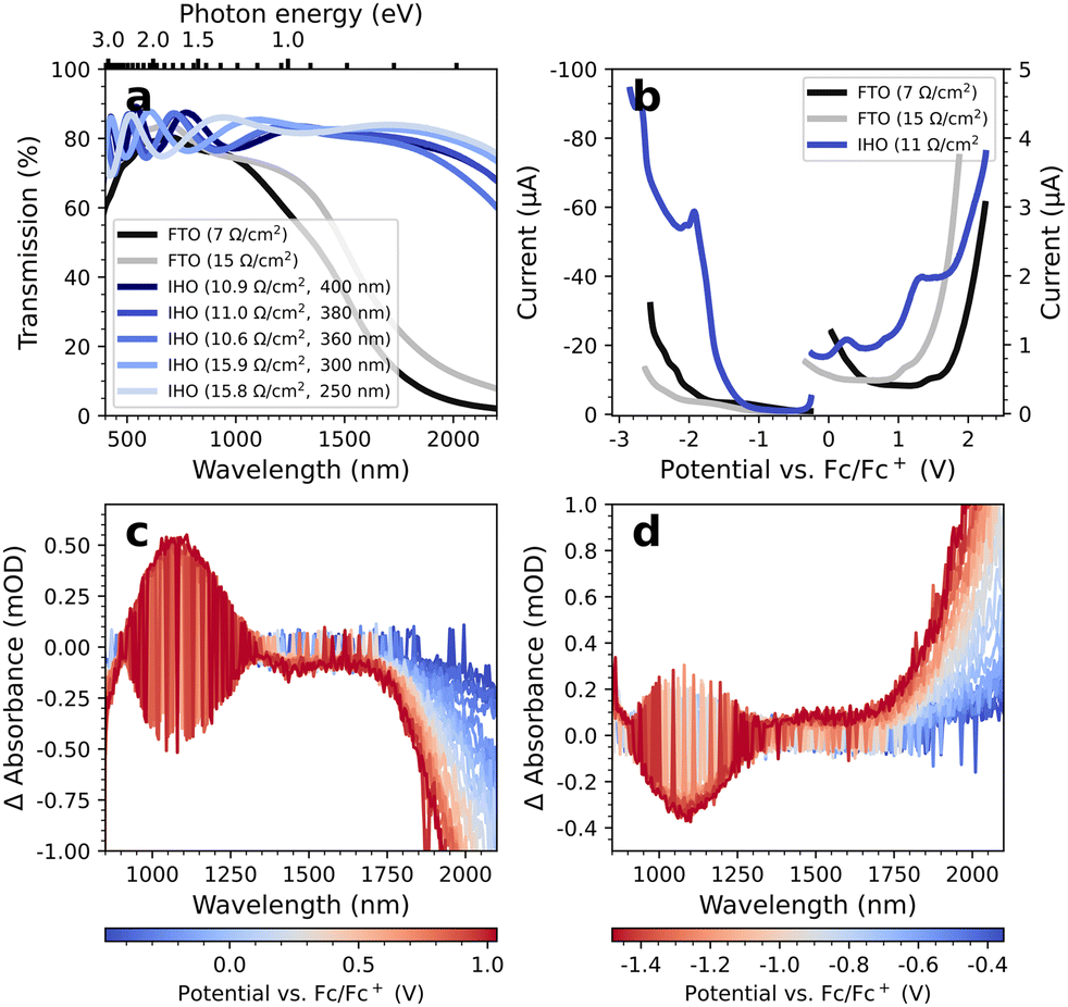 | ||
| Fig. 1 (a) Visible and NIR transmittance spectra of FTO substrates with sheet resistances of 7 and 15 Ω sq−1 and various IHO substrates. The respective preparation parameters can be obtained from Table S1.† (b) Reductive and oxidative DPV measurements of uncoated FTO and IHO substrates in LiClO4/MeCN-d3. (c) Oxidative and (d) reductive EMAS measurements of an uncoated IHO (11 Ω sq−1) with LiClO4/MeCN-d3 as electrolyte solution. | ||
Fig. 1b depicts the differential pulse voltammograms of an uncoated IHO substrate with a sheet resistance of 11 Ω sq−1 and two uncoated FTO substrates with sheet resistances of 7 and 15 Ω sq−1 measured in LiClO4/MeCN-d3. All differential pulse voltammetry (DPV) measurements were initiated at the respective open circuit potential (OCP), subsequently scanning to reductive and oxidative potentials. For both scan directions, a new spot on the substrate was chosen and the electrolyte solution was renewed. Although the FTO substrates show overall lower currents than the IHO electrode, we determine a large electrochemical measurement window of −1.5 to +1.5 V vs. Fc/Fc+ with the IHO electrode.
Fig. 1c and 1d display the oxidative and reductive EMAS spectra of an exemplary IHO substrate (see ESI† for the EMAS results of other IHO substrates). Noticeably, the oxidative spectra are mirrored images of the reductive spectra. Removing electrons from the material leads to less energetic plasmonic oscillations, indicated by the increasing bleach towards higher wavelengths. Overall, we note a weak differential absorbance (ΔA) below 1 mOD for the spectral range from 800–1900 nm and electrochemical potentials from −1.5 V to +1.0 V. Similar results are obtained in TBAHFP/MeCN-d3 (Fig. S3†). In comparison, the FTO substrates exhibit roughly an order of magnitude larger ΔA in the same range, including practically immeasurable conditions above 1800 nm (see Fig. S4 and S5†). Again, fine-tuning of the EMAS properties of the IHO electrodes is possible via the film thickness, e.g. shifting the ΔA-signal around 1100 nm to less critical spectral regions.
Optical and electrochemical properties of the PbS QDs
Fig. 2a shows the steady-state absorption spectra of the investigated PbS QDs with first excitonic transitions at 1474 nm (PbS-A, ∅5.5 nm), 1526 nm (PbS-B, ∅6.8 nm), 1656 nm (PbS-C, ∅7.3 nm), and 1729 nm (PbS-D, ∅8 nm).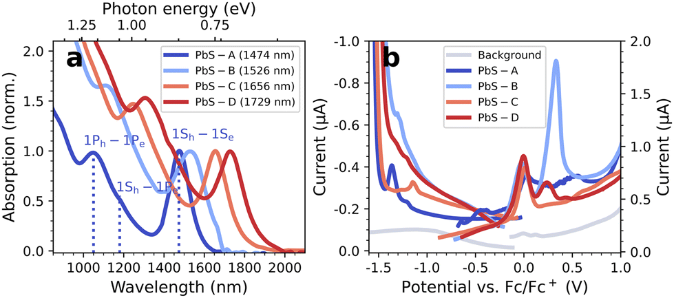 | ||
| Fig. 2 (a) Normalized absorption spectra and (b) DPV data of the PbS QDs. | ||
Fig. 2b depicts the DPV results of all PbS QDs measured in TBAHFP/MeCN on a glassy carbon (GC) electrode (coloured curves) compared to the background of a blank GC electrode (grey curve). The measurements were initiated at the respective OCPs and in each scan direction, new PbS material was applied. The DPV results illustrate the often-complicated interpretation of electrochemical characterizations of QDs: surface defects, ligand instabilities and high film resistances can invoke inconclusive DPV signals, limited reversibility and sluggish charge carrier injection. From a previous report,15 one would expect a reductive wave at roughly −0.8 eV (the conduction band edge) and, consequently, an oxidative wave at 0.0 V. While the latter is reflected in the data, an unambiguous assignment is challenging, and a clear reductive wave at the anticipated potential is missing entirely. Similar inconclusive results are obtained by complementary cyclovoltammetric experiments (see Fig. S6†). Overall, these difficulties already motivate the application of spectro-electrochemical techniques, such as EMAS, which can differentiate between band filling and electrochemical side reactions.1
Stability of the IHO electrodes and PbS QDs in the electrolyte
An inherent disadvantage of EMAS are the relatively long measurement times due to the lock-in amplification which requires a stepwise determination of ΔA for each wavelength. In Fig. 3, we test the stability of the IHO electrodes as well as the PbS QD films over typical measurement durations of 14 h in TBAHFP/MeCN-d3 without applying a bias. We find two notable changes: (1) the IHO absorption increases and (2) the excitonic transition of the PbS QDs undergoes a hypsochromic shift. Pure MeCN-d3 has no significant effect (see Fig. S7†). | ||
| Fig. 3 (a) Blank IHO before and after 14 h in TBAHFP/MeCN-d3. (b) PbS-A film on IHO before and after 14 h in TBAHFP/MeCN-d3. | ||
EMAS results of PbS QDs on IHO electrodes
We investigate the EMAS spectra of PbS-A on an IHO working electrode in TBAHFP/MeCN-d3 in the oxidative direction in Fig. 4a. Corresponding linecuts from these spectra at selected wavelengths are displayed in Fig. 4b. Spittel et al. have attributed the inflection point at 50% of the maximum ΔA-intensity to the position of the respective band edge.4 An alternative interpretation of such data by Vogel et al. uses the potential at the 1/8 ΔA-value based on the 8-fold degeneracy of the band edges.15 We follow the former interpretation, mainly due to a larger uncertainty in determining the 1/8 ΔA-level against the background in our data. We observe the formation of a bleach of the 1Sh–1Se transition (1470 nm) at −0.05 V vs. Fc/Fc+. The bleach of the 1Ph–1Pe transition (1050 nm) commences at approx. 0.0 V. Upon continuation to more oxidative potentials (and longer time in the electrolyte), the bleach shifts to shorter wavelengths until it saturates at 1350 nm. Resetting the potential to the open circuit potential and repeating the measurement results in a bleach at the new, shorter wavelength, indicating that the spectral shift is permanent (see Fig. S8†). We find a similar behaviour for the bleach of the 1Ph–1Pe transition, which shifts to 950 nm. The intensity of the 1Sh–1Se bleach exhibits a maximum, and the bleaches observed in repeated measurements of the same sample are generally weaker.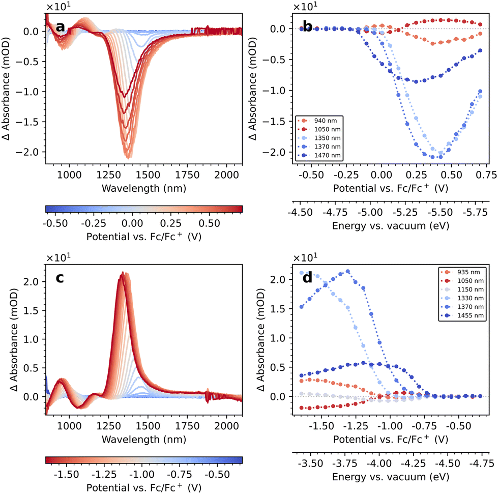 | ||
| Fig. 4 Oxidative (a) and reductive (c) EMAS measurement of PbS-A on IHO as working electrode and linecuts (b and d) at specific wavelengths. | ||
We display the corresponding EMAS results of the reductive direction in Fig. 4c. The line cuts at selected wavelengths in Fig. 4d exhibit an inflection point at approx. −0.85 V for the modulation of the 1Sh–1Se and the 1Ph–1Pe transitions, but their ΔA-values are now positive, that is, they constitute induced absorptions. Consistent with the oxidative EMAS results, we observe shifts of the ΔA-maxima to roughly 1350 nm and 950 nm, respectively.
Control experiments with PbS-B to PbS-D lead to similar results (see Fig. S9–S12†), only at slightly different potentials. Most notably, we find the general hypsochromic spectral shift and the induced absorption in the reductive scan direction in all EMAS measurements of PbS samples on IHO. Changing the electrolyte to LiClO4/MeCN-d3 results in comparable EMAS spectra (Fig. S13†).
We summarize the complete EMAS results for PbS-A to PbS-D in both scan directions in Fig. 5. Red colour indicates negative ΔA, while blue colour represents an induced absorption. The horizontal dashed lines mark the respective potentials at which 50% of the maximum ΔA is reached as determined by the inflection points in their linecuts at the wavelength of the excitonic transition. The vertical lines refer to characteristic transitions (e.g. 1Sh–1Se and 1Ph–1Pe) and are referenced to the second derivative of the corresponding absorption spectra from Fig. 2a. For PbS-A, we find a clean bandgap of roughly 0.8 eV, in accordance with the optical bandgap obtained by absorption spectroscopy. The inflection points for the positive (−0.05 V) and negative scan direction (−0.85 V) are largely consistent with Fig. 2b and Fig. S6b.† In contrast to the DPV results (Fig. 2b), there is no significant signal around −0.5 V, suggesting that this redox wave originated from an impurity not related to PbS. This emphasizes the power of spectroelectrochemistry with the ability to differentiate between such signals of different origin.
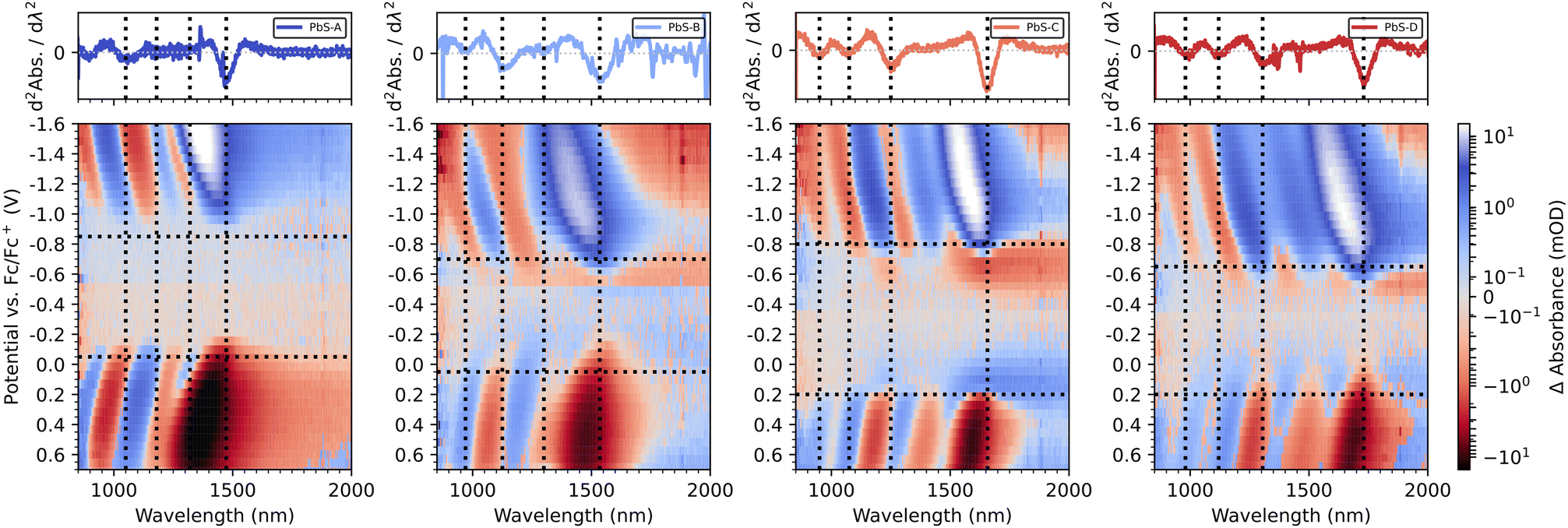 | ||
| Fig. 5 Combined reductive and oxidative EMAS spectra of PbS-A, PbS-B, PbS-C and PbS-D (from left to right). The top panel shows the second derivatives of the respective absorbance data. | ||
For PbS-B, we note overall similar EMAS results, however with some significant in-gap density of states, in particular near the valence band edge. Taking −0.70 V and +0.05 V as the inflection points of the conduction and valence band, respectively, (see Fig. S9† for details) suggests an Urbach-like tailing into the bandgap of approx. 250 meV from the valence band, which compares to less than 100 meV in the case of PbS-A. While it is unclear to which extent this result reflects the broader excitonic feature for PbS-B vs. PbS-A (see Fig. 2a) or a larger density of trap states, it emphasizes that EMAS can illustrate such sample-specific properties.
For PbS-C and PbS-D, the inflection points are at −0.8 V/+0.20 V and −0.65 V/+0.20 V, respectively (Fig. S10 and S11†), overestimating the optical bandgap by 0.25 eV and 0.13 eV. This appears to be the consequence of a relatively broad density of states in the vicinity of the band edges (particularly for PbS-C) that can even lead to a sign flip of the EMAS signal, rendering a precise determination of the inflection point challenging. A direct comparison of all EMAS spectra illustrates a consistent spectral shift in accordance with the different excitonic transition wavelengths for both scan directions (Fig. S12†).
Discussion
The EMAS results in Fig. 5 are evidence for the successful injection of electrons and holes into PbS to a similar degree. Hole injection into semiconductor QDs, in particular lead chalcogenides, is challenging presumably due to the smaller stability of holes.15,17 We argue that the relative ease with which this is achieved here originates in the periodically oscillating (67 Hz) potential applied to the film due to which holes are created for a comparably short time span. In addition, the IHO working electrodes provide a ΔA noise level on the order of 0.1 mOD, rendering this technique sensitive also for highly incomplete carrier injection.The induced absorption in the reductive direction found in all measurements here is counterintuitive and requires a more detailed discussion: we argue that it is the result of the long measurement time for each potential step (∼30 min) and limited stability of the QDs in the electrolyte (see Fig. 3). For each spectrum taken at a new potential, the absorption spectrum at the OCP is taken as a (new) reference, but if the background absorption during the following 30 min increases, a net-positive ΔA is possible. The 200 mOD increase in ΔA after 14 h (Fig. 3b) is supporting evidence that, on average, an increase on the order of 200/28 ≈ 7 mOD for each potential step by this process is plausible. The broadband increase in absorption in Fig. 3b hints toward additional scattering as the main reason for this change. Such scattering may be further impacted electrochemically, e.g. by reducing Pb2+ to Pb0 to form a strongly scattering layer around the QDs. In this scenario, the filling of the conduction band can result in a positive ΔA if the bleach due to Pauli blocking is overcompensated by the increase in background absorption.
To further verify our hypothesis, we reduce the integration time at each potential to 6 min by decreasing the spectral range. Additionally, the step width between the potentials is doubled to 120 mV to cut the total measurement time to ∼60 min for the whole scan. The corresponding EMAS spectra at reductive potentials are displayed in Fig. 6a.
 | ||
| Fig. 6 (a) EMAS spectrum of a smaller range measurements of PbS-A with phase plots at selected potentials (b–e). | ||
For −0.84 V (e.g. at/slightly below the conduction band edge), we observe a weak induced absorption. At larger potentials (e.g. −1.08 V), a prominent bleach occurs at the 1Sh–1Se transition. For even more negative potentials, S-shape EMAS spectra evolve, which indicate a hypsochromic shift, for instance due to partial QD etching. We obtain similar results with PbS-C, where fast reductive scans show a bleach of the excitonic transition until −1.2 V, after which S-shape EMAS spectra evolve (Fig. S14†). Consistent with this finding, we note that Vogel et al. have specified the stability window for PbS QDs to ≤−1.1 V.15
We continue with a discussion of the importance of the phase shift in EMAS for determining the sign of the differential absorption. ΔA is measured by a photodetector in terms of a corresponding differential photovoltage, ΔV, which is anti-correlated with ΔA (see Fig. S15†). Since a negative potential should result in negative ΔA, that is, positive ΔV, it follows that a textbook bleach is resembled by a phase shift of 180° between the oscillating potential and the oscillating ΔV recorded by the photodetector. Likewise, an induced absorption for reductive scans is resembled by a phase shift of 0° between the potential and ΔV. Since electrochemistry of QDs is sluggish, the ΔV-response will always lag behind these precise values to some extent. In Fig. 6b–e, this is taken into consideration by attributing all phase shifts from +45° to +180° to a bleach and all shifts from −135° to 0° to an induced absorption. In principle, these values are subjective and may lead to an erroneous attribution of the sign of ΔA. However, our results show that the phase behavior in the EMAS spectra in Fig. 6 is highly robust (for further examples, including those used for Fig. 5, see Fig. S16 and S17†). Except for the results with low amplitude, all phase shifts lie deep within their respective tolerance window with typical phase shifts for a bleach of +130° and −70° for induced absorption. We conclude that an erroneous phase attribution is unlikely to be the cause for the unusual induced absorption at the 1Sh–1Se transition in Fig. 4 and 5 for reductive potentials.
We further test our hypothesis that it is the measurement time and limited stability of the QDs in the electrolyte solution which causes the induced absorption for reductive scans. To this end, we freshly prepare four samples of PbS-A and measure each one 25 times at the same individual potential (∼30 min per measurement). At −0.48 V, e.g. close to the measured OCP, no features are visible (Fig. 7a). We emphasize that the total duration of this measurement is >12 h, and from Fig. 3, one would expect to see a significant increase in background absorption. We argue that the lock-in technique used here prevents the registration of such an erroneous signal: EMAS amplifies exclusively such signals that oscillate with the locked-in frequency. Because the increased background absorption is independent of the applied potential, it does not oscillate with the locked-in frequency, and it remains invisible in Fig. 7a.
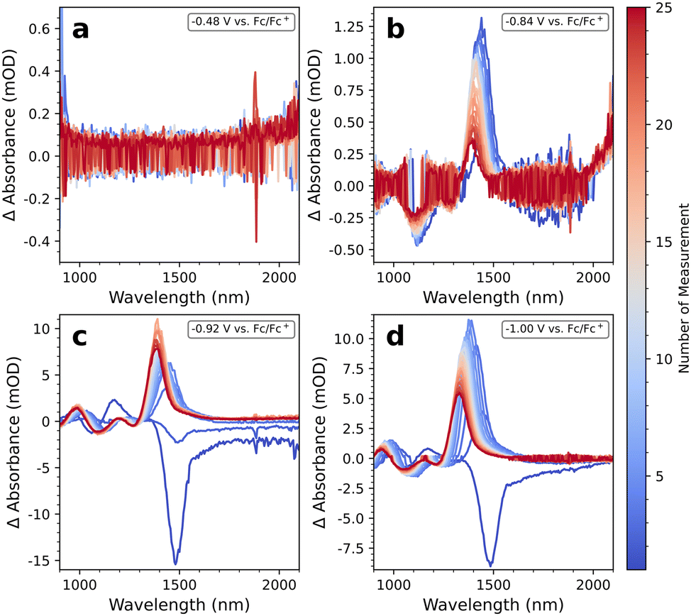 | ||
| Fig. 7 PbS-A measured 25 times at the same potential of (a) −0.48 V vs. Fc/Fc+, (b) −0.84 V vs. Fc/Fc+, (c) −0.92 V vs. Fc/Fc+, and (d) −1 V vs. Fc/Fc+. | ||
In contrast, at −0.84 V (Fig. 7b) there is a weak induced absorption with a magnitude of 1 mOD, in accordance with Fig. 6a. We argue that at this potential, there is a small density of states from the PbS conduction band that is filled/emptied with the locked-in frequency. Therefore, all absorption changes at this potential will be amplified. The total ΔA is the sum of the bleach due to Pauli blocking and the increased background absorption. If the density of states at this potential is small, the resulting ΔA will be positive. At −0.92 V we now observe the expected bleach of the 1Sh–1Se and 1Ph–1Pe transitions for the first two measurements before hypsochromic shifting and induced absorption sets in. The accessed density of states is larger at this potential, such that Pauli blocking overcompensates the increase in background absorption for the initial 2 × 30 min. At −1.0 V, dominating Pauli blocking prevails only during the first 30 minutes, presumably because an electrochemical process, such as the reduction of Pb2+ to Pb0 provides additional scattering. We also observe the same hypsochromic shifting to 1350 nm under these mild conditions as previously shown for the complete reductive scans.
Overall, these control experiments support our hypothesis that the induced absorption found in the reductive scan direction of all PbS QD samples are mostly due to the long exposure time in the electrolyte. We conclude that the measurement duration should be kept as short as possible, for instance by recording survey EMAS spectra first, followed by detailed spectra at selected wavelength ranges. An example is Fig. 4c, recorded over 14 h, and Fig. 6a, recorded over 60 min, with identical samples. Importantly, the potentials at which |ΔA| increases in both cases are almost the same.
Experimental
Fabrication of the IHO working electrodes
The IHO films were deposited on silica glass substrates by a radio frequency (RF) magnetron sputtering system (Beijing Technol Science Co., Ltd) at room temperature. A high-purity ceramic In2O3 target (Zhongnuo Advanced Material Technology Co., Ltd; 99.99%) was used as a sputtering target. At a base pressure of <10−4 Pa, an argon–hydrogen-gas mixture with a ratio of 99:1 and flow rates of 30 standard cubic centimetres per minute was introduced. After the gas pressure was stabilized at 0.22 Pa, a sputtering power of 150 W was applied for 20 to 35 min, resulting in a film thickness of 250 to 400 nm. The as-deposited IHO films were annealed at 280 °C for 90 seconds under N2. From the central part of each IHO coated glass slide, pieces of 2.5 × 6 cm are cut and cleaned in an ultrasonic bath by submersion in acetone and hexane for 15 min each and rinsed with isopropanol.
Synthesis of PbS quantum dots
The lead sulphide quantum dots (PbS QDs) were synthesized following a procedure introduced by Weidman, Tisdale et al. (2014).22 The concentration of the sulphur precursor was doubled in comparison to this method to increase the uniformity of the QDs due to faster injection. The sulphur precursor was prepared in a glovebox, by adding 80 mg elemental sulphur to 7.5 mL of dried oleylamine in a round-bottom flask and heating it to 100 °C for 60 min. The lead precursor was prepared by mixing 5 g of lead chloride (PbCl2) and 15 mL oleylamine and degassing at 120 °C for 1 h. Then, under nitrogen, 2.25 mL S-precursor were swiftly injected. After a specific reaction time, depending on the target size of the PbS QDs according to Weidman, Tisdale et al., the reaction was stopped by injection of cold n-hexane (97%, Extra Dry over Molecular Sieve, AcroSeal®, Acros Organics) and placing the flask in an ice bath. The PbS QDs were purified by injecting 5 mL EtOH (99.5%, Extra Dry, absolute, AcroSeal®, Acros Organics) and centrifuging for 10 min at 4000 rpm. The supernatant was discarded, and the precipitate was redissolved in 3 mL n-hexane. This washing cycle was repeated twice more. 3 mL of dried oleic acid were added to the cleaned particle solution. After stirring, 3 mL EtOH were added, followed by centrifugation for 5 min at 4000 rpm to remove excess oleic acid. The supernatant was discarded and the PbS particles were solved in 6 mL n-hexane.PbS sample preparation
The sample preparation and assembly of the spectroelectrochemical measurement cell were conducted inside a nitrogen filled glovebox. Before film preparation, the IHO substrates were cleaned by sonication in acetone and hexane for 15 min each and rinsing with isopropanol. A treatment with (3-aminopropyl)trimethoxysilane (APTMS) was performed by placing the substrates in a stirred 3% APTMS toluene solution at 50 °C for 90 min followed by rinsing with toluene. For the sample preparation of PbS-A, 500 μL of a 2 μM PbS solution in n-hexane was dropped on the conductive side of a slightly tilted IHO substrate. After evaporation of the solvent, the substrate with the now formed PbS film was dipped into a solution of 3% 1,2-ethanedithiol (EDT) in MeCN for 30 s and then rinsed with MeCN. The samples of PbS-B, PbS-C and PbS-D were prepared by dropping 100 μL of the respective 1.5 μM PbS solution in toluene onto the APTMS-coated IHO substrate and spincoating for 30 s at 10 rps with a 3 s ramp. Afterwards, the sample was dried at 50 °C followed by spincoating 200 μL of a 3% EDT/MeCN solution onto the substrate and washing with MeCN. These steps were repeated until a homogenous, transparent yet clearly visible film is gained.To ensure good contacting, the upper 25% of all IHO substrates was left uncoated.
Electrolyte solutions
The electrolyte n-Bu4NPF6 (TBAHFP, 98%, Alfa Aesar) was recrystallized five times from 3:1 EtOH/H2O and dried for 6 days at 105 °C and 2–3 mbar. The purity was checked by 1H-, 13C-, 19F-, and 31P-NMR spectroscopy. The electrolyte LiClO4 (battery grade, 99.99% trace metal basis, Sigma Aldrich), AgClO4 (≥97%, anhydrous, Alfa Aesar) and Ferrocene (98%, Acros Organics) were used without further purification. Deuterated acetonitrile CH3CN-d3 (MeCN-d3; >99.8 atom % D) was purchased from Sigma Aldrich, and a 0.1 M electrolyte solution was prepared using the respective electrolyte. All chemicals used for electrochemical experiments were stored and handled under N2 atmosphere.
Differential pulse voltammetry (DPV)
DPV measurements were performed in a nitrogen-filled glovebox under inert conditions with a CHI760E Bipotentiostat (CH-Instruments). The PbS experiments were performed using a full-glass gas-tight electrochemical cell, which was additionally placed in a Faraday cage to shield from environmental electromagnetic radiation. The used three-electrode setup consisted of a 3 mm diameter glassy carbon disc electrode (Metrohm 6.1204.300 GC) as a working electrode, a 1 mm diameter coiled platinum wire as a counter electrode, and a Haber–Luggin double-reference electrode composed of an Ag/Ag+ system (1 mm diameter silver wire in a 0.01 M AgClO4 solution in 0.1 M TBAHFP/MeCN), which was capacitively coupled (10 nF) to a Pt wire which was immersed into the electrolyte next to the capillary opening. To prevent contaminations of the electrolyte within the sample chamber by the reference electrode solution, an additional frit filled with 0.1 M TBAHFP/MeCN was inserted between the Haber Luggin capillary and the reference electrode compartment. The sample chamber of the electrochemical cell was filled with 12 mL of 0.1 M TBAHFP/MeCN.Measurements were carried out starting at the OCP of the blank GC electrode to −2.8 V in reductive, and to 2 V in oxidative direction. Scans were performed with a potential step width of 4 mV, 50 mV amplitude, 0.06 s pulse width, 0.02 s sample width, and a 0.5 s pulse period at a measurement sensitivity of 10 μA V−1. The integrated positive feedback function of the CHI760E bipotentiostat was used for iR-compensation at a compensation level of 82%. At first, background scans were performed with a freshly polished GC disc electrode. Afterward, 10 μL of the respective 1.5 μM PbS solutions in n-hexane were dropcasted on the freshly cleaned GC working electrode. Sample measurements were performed in reductive and oxidative direction with the same parameters as the background scans and freshly prepared PbS coatings were used for each measurement.
The applied potential values of all measurements were converted to the formal potential of the external redox couple ferrocene/ferrocenium (Fc/Fc+), which was measured at 83 mV versus Ag/Ag+ within the same cell setup used for DPV measurements.
The DPV measurements of the blank FTO-coated glass substrates (Solaronix, TCO22-15, thickness 2.2 mm, sheet resistance 15 Ω sq−1; Sigma Aldrich, 735167, thickness 2.2 mm, sheet resistance 7 Ω sq−1) and IHO substrates were performed inside the EMAS cell filled with LiClO4/MeCN-d3 and referenced to the respective Ferrocene values given in the ESI (see Fig. S18†) and below.
Cyclic voltammetry (CV)
CV measurements were performed in the same full-glass electrochemical cell setup as the DPV measurements.Measurements were started at the respective OCP and performed as six segments with a scan rate of 0.01 V s−1, sample intervals of 1 mV and a sensitivity of 10 μA V−1. For oxidative scans, the high potential was set at 0.7 V, reductive scans were done up to −0.8 V, −1 V and −1.6 V. The iR-compensation of the CHI760E bipotentiostat was used at a compensation level of 82%. Background scans were performed with a freshly polished GC working electrode. For each PbS measurement 10 μL of the respective 1.5 μM PbS solution was freshly dropcasted onto the clean GC electrode. The applied potentials were referenced against an Fc/Fc+ value of 83 mV.
Potential-modulated absorption spectroscopy (EMAS)
A home-built spectroelectrochemical transmission cell was equipped with a 1 mm diameter Ag wire pseudoreference electrode, a 1 mm diameter coiled platinum wire counter electrode, and an IHO or FTO coated glass as the working electrode. The working electrode was either uncoated for background measurements or coated with a PbS QD film. The measurement cell was assembled in a nitrogen-filled glovebox and either filled with 6 mL 0.1 M TBAHFP/MeCN-d3 or with 0.1 M LiClO4/MeCN-d3. After assembly, it was transferred outside of the glovebox and placed in a Faraday cage for the EMAS measurements.A constant potential at the respective, previously measured OCP was applied to the working electrode using the CHI760E bipotentiostat. A rectangular-shaped modulated potential, produced by a Waveform generator (PSG9080, Joy-IT), with a modulation frequency of 67 Hz and a variable amplitude as an offset was superimposed. Meanwhile, the working electrode was transilluminated by monochromatic light generated by a QTH lamp (Apex2, Oriel Instruments) of wavelengths selected by a monochromator (Cornerstone 130, Oriel Instruments). At certain wavelengths long-pass filters (570 nm and 1000 nm) were introduced into the beam path to block components with a higher diffraction order. The transmitted light was detected by an InGaAs detector (Thorlabs, DET05D), and the signal was passed to a lock-in amplifier (MFLI, Zurich Instruments). In parallel, the lock-in amplifier received the modulated potential generated by the signal generator as a reference signal and searched for a modulated component in the optical signal that oscillated at the same frequency. In the ESI a detailed schematic illustration of the EMAS setup is included (see Fig. S19†).
Considering the phase relationship between the modulated potential and the modulated component in the optical signal, it was determined whether the measured signal was an induced absorption or a bleach (for more information, see the discussion section). During the EMAS measurement, the modulated potential component was applied to the sample in such a way that the total potential always oscillated between the respective OCP and a corresponding reductive or oxidative potential. At the beginning of the measurement, the peak-to peak amplitude was 60 mV. With an appropriate offset, the signal was then shifted to positive or negative values, so that the potential was modulated between OCP and OCP ± 60 mV. At this potential, a complete spectrum from 850 to 2100 nm was scanned in 5 nm steps. Afterward, the peak-to-peak amplitude was increased by 60 mV, the signal offset was adjusted accordingly, and a complete spectrum was recorded again. This was repeated until the final corresponding oxidative or reductive potential was reached. During the EMAS measurement, iR-compensation by the integrated positive feedback function of the CHI760E was activated and a compensation level of 92% was chosen. The measurement sensitivity of the bipotentiostat was set to 0.1 mA V−1 and the AC-coupled signal input of the lock-in amplifier was set to 10 MΩ with an input range of 10 mV. Incoming signals were processed by a 6th-order low-pass filter having a time constant of 100 ms. The resolution of the monochromator was set to 5–7 nm by setting the input and output slit width to 400 μm. The potential of the measured data was also converted to the formal potential of the external redox couple ferrocene/ferrocenium (Fc/Fc+), which was measured at 357 mV versus Ag pseudoreference electrode for IHO substrates in 0.1 M TBAHFP/MeCN-d3, at 247 mV versus Ag pseudoreference electrode for IHO substrates in 0.1 M LiClO4/MeCN-d3, at 256 mV versus Ag pseudoreference electrode for FTO substrates (7 Ω sq−1) in 0.1 M LiClO4/MeCN-d3, and 629 mV versus Ag pseudoreference electrode for FTO substrates (15 Ω sq−1) in 0.1 M LiClO4/MeCN-d3 within the same setup.
Other experimental techniques
The electrical properties were measured by Hall effect measurements (HMS-7000, Ecopia), with a magnetic field of 0.55 T and an operating current of 15 mA.SEM measurements were performed using a Hitachi SU 8030 (see Fig. S20†).
The approximate height of the PbS thin films was determined with a Bruker Dektak XT-A stylus profilometer with a stylus force of 3 mg, a stylus scan range of 6.5 μm and stylus radius of 2 μm (see Fig. S21†).
The absorption measurements were carried out with a Cary 5000 UV-Vis-NIR spectrophotometer (Agilent Technologies; slit height: full; spectral bandwidth: 2 nm). For measurements with IHO substrates a special holder was used (for results see Fig. S22†).
Ultraviolet photoelectron spectroscopy (UPS) was conducted with a Thermo Fisher Scientific ESCALAB XI+, with He Iα radiation at 21.22 eV (see Fig. S23†).
X-ray photoelectron spectroscopy (XPS) was carried out with a Thermo Scientific K-Alpha spectrometer with Al Kα radiation at 1486.6 eV (see Fig. S24†).
The X-ray diffraction (XRD) pattern was acquired using a Rigaku Ultima X-ray diffractometer with Cu Kα radiation (40 kV, 40 mA) with a scan rate of 10° min−1 (see Fig. S25†).
Conclusions
We have imaged the electrochemically excited-state absorption of ethanedithiol-crosslinked PbS quantum dot films with excitonic transitions between 1470 nm and 1730 nm. Electron and hole injection was successfully achieved, the absolute positions of the conduction and valence band were determined, and the band gap was illustrated. These results are enabled by the combination of potential-modulated absorption spectroscopy with working electrodes made from hydrogen-doped indium oxide. With this combination, we achieve a noise level for the differential absorption of 0.1 mOD between 1300 nm and 1750 nm, which provides the required sensitivity for monitoring the often incomplete and irreversible electrochemical excitation of quantum dots. Increasing the thickness of the doped indium oxide enables a similar sensitivity up to 2000 nm, rendering the technique presented here a powerful tool for elucidating the density of states in the vicinity of the band gap of IR-active quantum dot materials.Author contributions
M.S. and B.H. initiated and supervised the project. S.L. fabricated the IHO substrates and performed UPS, XPS, XRD, and Hall effect measurements. P.M. synthesized and purified the PbS QDs. S.W. planned and performed the spectroscopic and (spectro-)electrochemical experiments and the data analysis. S.W. and M.S. co-wrote this manuscript with input from all authors.Data availability
The data supporting this article have been included as part of the ESI.†Conflicts of interest
There are no conflicts to declare.Acknowledgements
Financial support of this work has been provided by the Heinrich-Böll Stiftung with a PhD scholarship to SW, by the Deutsche Forschungsgemeinschaft (DFG) under grant SCHE1905/9-1 (project no. 426008387) and the National Natural Science Foundation of China (62274071 and 52192612). SEM measurements were performed by Elke Nadler (University Tübingen).References
- M. Weber, S. Westendorf, B. Märker, K. Braun and M. Scheele, Phys. Chem. Chem. Phys., 2019, 21, 8992–9001 RSC.
- J. Poppe, S. G. Hickey and A. Eychmüller, J. Phys. Chem. C, 2014, 118, 17123–17141 CrossRef CAS.
- J. Garoz-Ruiz, J. V. Perales-Rondon, A. Heras and A. Colina, Isr. J. Chem., 2019, 59, 679–694 CrossRef CAS.
- D. Spittel, J. Poppe, C. Meerbach, C. Ziegler, S. G. Hickey and A. Eychmüller, ACS Nano, 2017, 11, 12174–12184 CrossRef CAS PubMed.
- S. C. Boehme, H. Wang, L. D. A. Siebbeles, D. Vanmaekelbergh and A. J. Houtepen, ACS Nano, 2013, 7, 2500–2508 CrossRef CAS PubMed.
- J. J. Geuchies, B. Brynjarsson, G. Grimaldi, S. Gudjonsdottir, W. van der Stam, W. H. Evers and A. J. Houtepen, ACS Nano, 2021, 15, 377–386 CrossRef CAS PubMed.
- D. Yu, C. Wang and P. Guyot-Sionnest, Science, 2003, 300, 1277–1280 CrossRef CAS PubMed.
- S. Gudjonsdottir, W. van der Stam, N. Kirkwood, W. H. Evers and A. J. Houtepen, J. Am. Chem. Soc., 2018, 140, 6582–6590 CrossRef CAS PubMed.
- S. C. Boehme, J. M. Azpiroz, Y. V. Aulin, F. C. Grozema, D. Vanmaekelbergh, L. D. A. Siebbeles, I. Infante and A. J. Houtepen, Nano Lett., 2015, 15, 3056–3066 CrossRef CAS PubMed.
- W. van der Stam, I. du Fossé, G. Grimaldi, J. O. V. Monchen, N. Kirkwood and A. J. Houtepen, Chem. Mater., 2018, 30, 8052–8061 CrossRef CAS PubMed.
- K. M. Wurst, O. Strolka, J. Hiller, J. Keck, A. J. Meixner, J. Lauth and M. Scheele, Small, 2023, 19, 2207101 CrossRef CAS PubMed.
- J. T. Mulder, I. du Fossé, M. Alimoradi Jazi, L. Manna and A. J. Houtepen, ACS Energy Lett., 2021, 6, 2519–2525 CrossRef CAS PubMed.
- W. van der Stam, M. de Graaf, S. Gudjonsdottir, J. J. Geuchies, J. J. Dijkema, N. Kirkwood, W. H. Evers, A. Longo and A. J. Houtepen, ACS Nano, 2018, 12, 11244–11253 CrossRef CAS PubMed.
- W. van der Stam, S. Gudjonsdottir, W. H. Evers and A. J. Houtepen, J. Am. Chem. Soc., 2017, 139, 13208–13217 CrossRef CAS PubMed.
- Y. B. Vogel, L. N. Pham, M. Stam, R. F. Ubbink, M. L. Coote and A. J. Houtepen, J. Am. Chem. Soc., 2024, 146, 9928–9938 CrossRef CAS PubMed.
- S. C. Boehme, D. Vanmaekelbergh, W. H. Evers, L. D. A. Siebbeles and A. J. Houtepen, J. Phys. Chem. C, 2016, 120, 5164–5173 CrossRef CAS.
- B. L. Wehrenberg and P. Guyot-Sionnest, J. Am. Chem. Soc., 2003, 125, 7806–7807 CrossRef CAS PubMed.
- H. Lu, G. M. Carroll, X. Chen, D. K. Amarasinghe, N. R. Neale, E. M. Miller, P. C. Sercel, F. A. Rabuffetti, A. L. Efros and M. C. Beard, J. Am. Chem. Soc., 2018, 140, 13753–13763 CrossRef CAS PubMed.
- E. Yang and B. Hu, J. Phys.: Conf. Ser., 2023, 2510, 012011 CrossRef CAS.
- C. Ge, E. Yang, X. Zhao, C. Yuan, S. Li, C. Dong, Y. Ruan, L. Fu, Y. He, X. Zeng, H. Song, B. Hu, C. Chen and J. Tang, Small, 2022, 18, 2203677 CrossRef CAS PubMed.
- S. Li, E. Yang, Y. Li, X. Mo, Z. Chen, Z. Zhou, G. Tao, Y. Long and B. Hu, Nano Energy, 2024, 129, 110023 CrossRef CAS.
- M. C. Weidman, M. E. Beck, R. S. Hoffman, F. Prins and W. A. Tisdale, ACS Nano, 2014, 8, 6363–6371 CrossRef CAS PubMed.
Footnotes |
| † Electronic supplementary information (ESI) available: Further characterization of TCO electrodes, CV measurements, linecuts of EMAS spectra, SEM images and profilometry of thin films. See DOI: https://doi.org/10.1039/d4nr05347h |
| ‡ These authors contributed equally. |
| This journal is © The Royal Society of Chemistry 2025 |