
 Open Access Article
 This Open Access Article is licensed under a Creative Commons Attribution-Non Commercial 3.0 Unported Licence
Emerging 15–16 group Xenes: structures, properties, preparation methods, and their catalytic applications
Cong
Ma†
 a,
Kai
Bao†
a,
Junlei
Qi
a,
Wenbin
Wang
a,
Jingkun
Wu
a,
Ruijie
Li
a,
Yu
Lin
a,
Lingzhi
Wang
a,
Zhuangzhuang
Yin
a,
Zhixiang
Tao
a,
Chengxuan
Ke
ab,
Zongxiao
Wu
a,
Yingxia
Liu
*c and
Qiyuan
He
*a
a,
Kai
Bao†
a,
Junlei
Qi
a,
Wenbin
Wang
a,
Jingkun
Wu
a,
Ruijie
Li
a,
Yu
Lin
a,
Lingzhi
Wang
a,
Zhuangzhuang
Yin
a,
Zhixiang
Tao
a,
Chengxuan
Ke
ab,
Zongxiao
Wu
a,
Yingxia
Liu
*c and
Qiyuan
He
*a
aDepartment of Materials Science and Engineering, City University of Hong Kong, 83 Tat Chee Avenue, Kowloon, Hong Kong, China. E-mail: yingxliu@cityu.edu.hk
bDepartment of Materials Science and Engineering, Southern University of Science and Technology, Xueyuan Avenue 1088, Shenzhen, China
cDepartment of Systems Engineering, City University of Hong Kong, 83 Tat Chee Avenue, Kowloon, Hong Kong, China. E-mail: qiyuanhe@cityu.edu.hk
First published on 16th February 2025
Abstract
Elemental two-dimensional (2D) materials, commonly referred to as Xenes, have attracted recent attention due to their many unique/remarkable chemical and physical properties. Xenes hold immense promise for multifarious applications across diverse domains, including optoelectronics, energy storage, energy conversion and biomedicine. Beyond graphene and phosphorene, a new cadre of Xenes has emerged, with particular attention directed toward antimonene, arsenene, tellurene and selenene. These nascent Xenes have garnered substantial interest due to their diverse allotropes, as well as their distinctive layer-dependent and modifiable properties, rendering them highly adaptable for engineering and catalytic applications. Herein, an overview is provided for the recent advancements in the structures, inherent properties and degradation behavior of Xenes, drawing upon both theoretical and experimental research. The synthesis methods of Xenes are summarized and primarily classified as bottom-up and top-down approaches. Furthermore, the catalytic potential of Xenes is elaborated, emphasizing both engineering strategies and theoretical understanding toward enhanced performance across a spectrum of catalytic reactions. Conclusively, a summary and perspectives on the future development of Xenes are given to boost their development.
 Cong Ma | Cong Ma received her BEng. degree and MEng. degree from Tianjin University. Then she moved to the Department of Materials Science and Engineering Department in the City University of Hong Kong in 2023 to pursue her PhD under the supervision of Prof. Qiyuan He. Her research interests mainly include 2D materials and devices. |
 Qiyuan He | Dr Qiyuan He is currently an Associate Professor in the Department of Materials Science & Engineering at the City University of Hong Kong. He obtained his PhD Degree from Nanyang Technological University in Singapore and did his postdoc work in the University of California, Los Angeles. Dr He's research scope focuses on the fundamentals of semiconductor interfaces and their applications in nanoelectronics, iontronics, catalysis and on-chip electrochemistry. He has published over 100 research papers with over 24,000 citations with an H-index of 58 (SCOPUS). He has also been listed as Stanford's top 2% most highly cited scientist and a Highly Cited Researcher (cross-field) by Clarivate. |
1. Introduction
Two-dimensional (2D) materials are attracting extensive research interest across multiple disciplines, primarily due to their unique yet remarkable characteristics, including atomic thinness,1–3 large surface area,1,4,5 morphology tunability,4,6 structural anisotropy,7,8 excellent mobility4,9,10 and good mechanical flexibility,2,11,12 and the convenience to customize the surface characteristics for diverse applications.4 Among the vast 2D material family, elemental 2D materials belong to a developing branch of graphene-like 2D materials, commonly called “Xenes”.13 Xenes consist of one single element from the 13–17 groups in the periodic table, generally characterized by a layered architecture and large surface area similar to graphene,14 encompassing metals, semi-metals and non-metals.15 It is worth mentioning that α-phase and β-phase tellurene and selenene are intrinsically 1D materials in nature, composed of one-dimensional atomic chains. Therefore, they are classified as quasi-2D Xenes in this work,11,12,15 where a van der Waals interface between each layer can be observed and utilized in both chemical synthesis and exfoliation.Xenes have many intriguing properties. One particularly notable and attractive aspect is their ability to modulate bandgaps through various surface engineering techniques, which contribute to multiple applications, including electronics, optoelectronics, sensors, energy storage, energy conversion, and biomedicine.14 Among Xenes, black phosphorene (BP) is particularly attractive and well-developed because of ultrahigh carrier mobility, tunable bandgap, and abundant active sites, which are favorable for catalysis. Nevertheless, the utility of BP is influenced by its susceptibility to degradation in water and air due to the vulnerability of its lone electron pair to ambient environments. Other elemental 2D materials within groups 15 and 16, such as arginine, antimonide, telluride, and selenite with BP-like marked puckered structures, have also attracted increasing attention in recent years due to their diverse crystal structures and properties and, more importantly, superior stability under ambient conditions.15
Several comprehensive reviews have been published on the Xenes family. Their myriad applications, including electronics,16–18 optoelectronics,13,16–18 energy storage,16–18 and conversion,16,17,19 as well as biological applications,16,20,21 picturing a vibrant research field. In addition, in-depth examinations are conducted for Xenes that attract extensive attention, such as phosphorene22,23 and borophene.24,25 Alternatively, this review focuses exclusively on the emerging research of Xenes from groups 15 and 16, including antimonene, arsenene, tellurene and selenene. These four emerging Xenes, located within groups 15 and 16, exhibit similar electron-structural properties owing to their adjacency within the periodic table, and exhibit tunable electronic band structures and high carrier mobilities16,18 and more importantly satisfactory stability compared to black phosphorous in the ambient environment.
Recently, there have been increasing studies on the roles of Xenes in clean energy applications, especially as electrocatalysts owing to the large specific surface area,4,5,17 high electron transfer ability,26,27 tunable electron density28,29 and robust structural stability.16,30 However, as emerging 2D materials, the true potential of Xenes in the field of catalysis remains ambiguous. This review mainly discusses the emerging group 15 and 16 Xenes and their latest advancements in the past five years. Their commonalities and differences in structures, preparation methods, engineering approaches and catalytic applications are summarized and discussed as shown in Fig. 1. These insights offer a forward-looking perspective on the fundamental exploration and prospective application of Xenes' intriguing materials.
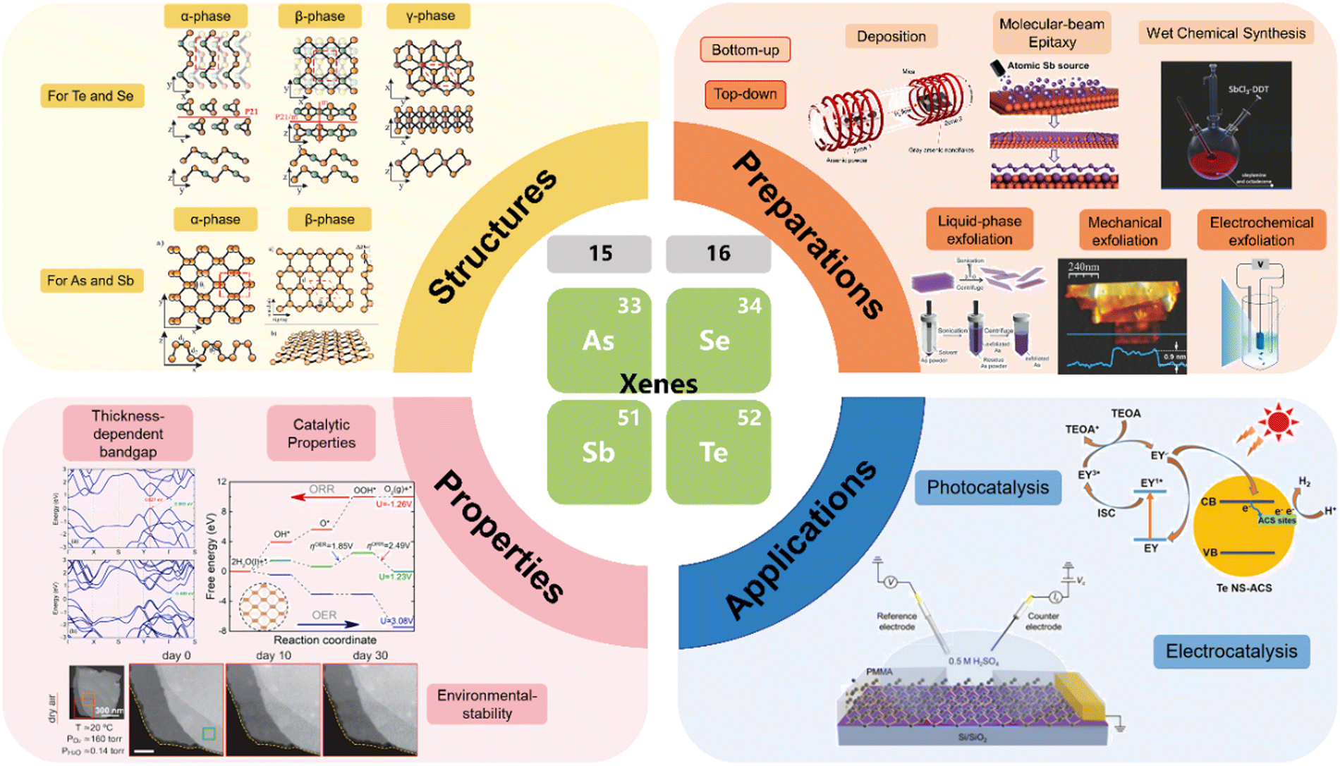 | ||
| Fig. 1 Schematic of the review, illustrating the structures,31 preparation methods (deposition,32 molecular beam epitaxy,33 wet-chemical synthesis,34 liquid-phase exfoliation,2 mechanical exfoliation35 and electrochemical exfoliation26), properties (thickness-dependent bandgap,36 catalytic properties37 and environmental-stability38) and applications (photocatalysis39 and electrocatalysis27) of emerging group 15 and 16 Xenes. Reproduced from ref. 31 with permission from Royal Society of Chemistry, Copyright 2021; reproduced from ref. 32 with permission from American Chemical Society, Copyright 2019; reproduced from ref. 33 with permission from WILEY-VCH, Copyright 2019; reproduced from ref. 34 with permission from WILEY-VCH, Copyright 2019; reproduced from ref. 2 with permission from WILEY-VCH, Copyright 2019; reproduced from ref. 35 with permission from Wiley-VCH, Copyright 2016; reproduced from ref. 26 with permission from WILEY-VCH, Copyright 2021; reproduced from ref. 36 with permission from Springer Nature, Copyright 2015; reproduced from ref. 37 with permission from American Chemical Society, Copyright 2021; reproduced from ref. 38 with permission from American Chemical Society, Copyright 2020; reproduced from ref. 39 with permission from Wiley-VCH, Copyright 2023; reproduced from ref. 27 with permission from WILEY-VCH, Copyright 2020. | ||
2. Layered structures and properties
Antimonene, arsenene, tellurene and selenene exhibit various phases, evident in both experimental synthesis and theoretical predictions. These Xenes can display semiconducting and metallic properties, as well as indirect–direct bandgap transitions, depending on their phase and layer number. Diverse atomic structures combined with the electronic characteristics of these emerging Xenes facilitate their extensive applications in energy conversion. In this review, we primarily focus on the phases that exhibit high chemical stability, and their structural properties are summarized in Table 1 and Fig. 2.| Materials | Structures | Thickness (nm) | Monolayer height (Å)/interlayer distance (Å) | Lattice parameters (Å) | Electronic property/bandgap | Synthetic methods | Ref. |
|---|---|---|---|---|---|---|---|
| Vitreous arsenene | Amorphous (a regular hexagonal shape) | — | — | — | p-Type semiconducting (0.09–0.32 eV) | Wet chemistry vitrification | 40 |
| β-Arsenene | Rhombohedra (a regular hexagonal shape) | 4–48 | — | — | Semimetallic (pristine three-layer gray arsenene) | van der Waals epitaxy on mica | 40 |
| β-Arsenene | Rhombohedral | 4 | — | — | — | van der Waals epitaxial growth on mica | 32 |
| β-Arsenene monolayer | Buckled honeycomb | — | — | a = b = 3.6 | Semiconducting | Grown on Ag (111) | 41 |
| β-Arsenene | Rhombohedral | 5–12 | 1.35 (buckling height), 2.04 (interlayer distance) | a = b = 3.76 | — | Liquid-phase exfoliation (in organic and aqueous solvents using a tip sonication system) | 2 |
| α-Arsenene | Orthorhombic | ≈0.6 | — | — | — | Low-potential electrochemical exfoliation | 42 |
| β-Antimonene | Buckled honeycomb | — | 1.78 (buckling height) | a = 3.84 | 0.11 eV (compressive-strained antimonene on Sb–Cu (110)) | Grown on Cu (110) by MBE | 33 |
| β-Antimonene | Buckled honeycomb | 1.42 (buckling height) | a = 4.43 | 0.21 eV (tensile-strained antimonene on Sb–Cu (111)) | Grown on Cu (111) by MBE | 33 | |
| β-Antimonene | ≈4 nm in suspension, 2 μm thickness coating on TiO2 film | — | — | The hole acceptor layer in PEC | Liquid-phase exfoliation from bulk Sb crystal, and then using electrophoretic deposition on TiO2 films | 43 | |
| β-Antimonene | — | 1.71 | — | — | 1.57 eV (optical bandgap) | Li+ intercalation and ultrasonication | 44 |
| β-Antimonene | — | 4–17, average 10 | 9 | — | — | A combination of ball milling and sonication-based liquid exfoliation | 45 |
| β-Antimonene | Rhombohedral | 46 | — | — | — | Soft-template assisted synthesis in colloidal solutions (SbCl3 dissolves in alkyl phosphonic acids) | 46 |
| α-Antimonene monolayer | Puckered structure | 1–20 layers | ≈0.78 | a = 4.4, b = 4.8 | Metallic | Grown on Td-WTe2 by MBE | 1 |
| α-Antimonene monolayer | Puckered honeycomb | 1–3 layers | — | a = 4.46, b = 4.87 | Monolayer, bilayer and trilayer antimonene/MoTe2 are all metallic | Grown on Td-MoTe2 by MBE | 47 |
| α-Antimonene monolayer | Puckered honeycomb | Stay α-phase to ≈15 layers | — | a = 4.29, b = 4.76 | Semiconducting ≈0.17 eV (nearly freestanding monolayer), a semiconductor-semimetal crossover in bilayer α-Sb | Grown on SnSe by MBE | 47 |
| α-Selenene | Buckled non-planar | ≈0.6–0.7 | ≈0.3 | a = b = 4.92 and c = 5.05 (bulk) | Intrinsic p-type conductivity, ideal bandgap for visible light absorption (≈1.6 eV) | Grown on the silicon by CVT | 48 |
| α-Tellurene | Chiral-chain lattice stacked up by helical chains | 10–50 | — | — | — | Grown on exfoliated 1T′-MoTe2 by ultrasonication-assisted synthesis | 9 |
| α-Tellurene | Helical | Micrometer level | 4.45 Å (distance between Te chains) | — | High hole mobility | Grown on 1T′-MoTe2 as the template by CVD | 49 |
| α-Tellurene | — | ≈15 | — | a ≈ b ≈ 4.39 Å | — | Grown on SrTiO3 (STO) by MBE | 50 |
| α-Tellurene | >100 | Unipolar p-type transport | Grown on SiO2/Si by CVD | 39 | |||
| α-Tellurene | A helical chain | 8–30 | — | 0.3![[thin space (1/6-em)]](https://www.rsc.org/images/entities/char_2009.gif) eV (bulk), 0.6eV (4.5 nm-thick evaporated Te films) (optical bandgap), p-type mobility eV (bulk), 0.6eV (4.5 nm-thick evaporated Te films) (optical bandgap), p-type mobility |
Thermal evaporation at cryogenic temperatures | 51 | |
| α-Tellurene | 12–20 | 10–90 | The interlayer spacing is ≈2.2 and 6, corresponding to the (1![[2 with combining macron]](https://www.rsc.org/images/entities/char_0032_0304.gif) 10) and (0001) planes. 10) and (0001) planes. |
— | Unipolar p-type transport | Hydrothermal | 39 |
| α-Tellurene | Bundles helical chains | ≈27 | The interplanar spacings 1.9 and 2.8, corresponding to Te (1210) and (0001) planes | — | Indirect bandgap (0.17 eV, bulk), indirect bandgap (0.27 eV, the synthesized Te), high hole mobilities | Hydrothermal | 52 |
| α-Tellurium | Three-fold screw-symmetric atomic chains | 10–20 | — | — | n-Type semiconducting | Hydrothermal | 53 |
| β-Tellurene | Helical chains with threefold screw symmetry | ≈0.4–0.8 | Lattice spacings of ≈0.193 nm, and ≈0.225 nm, corresponding to the (200) and (110) planes | Indirect bandgap (bulk crystal), 0.09 eV (bulk) to 1.27 eV (monolayer), p-type semiconducting | Grown on WS2 by vdW epitaxy | 54 | |
| γ-Tellurene | Hexagonal | Nanometer level | 0.7 eV (monolayer) | PVD | 3 |
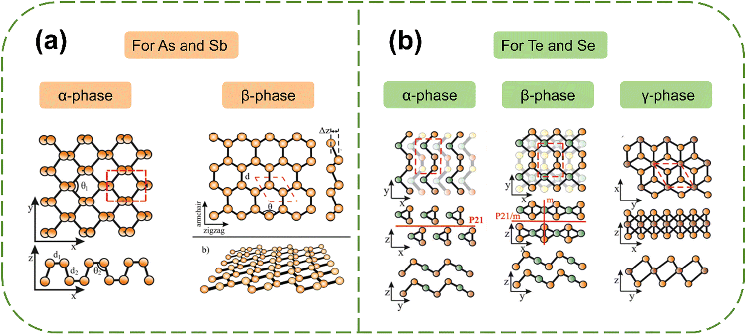 | ||
| Fig. 2 Structures of antimonene, arsenene, tellurene and selenene. (a) α-phase and β-phase for arsenene or antimonene. (b) α-phase, β-phase and γ-phase for selenene and tellurene.31 Reproduced from ref. 31 with permission from Royal Society of Chemistry, Copyright 2021. | ||
2.1 Group 15 Xenes
Group 15 elements, arsenic (As) and antimony (Sb), have electron configurations of 4s24p3 and 5s25p3, respectively, with five valence electrons. These elements require three additional electrons to achieve a stable octet configuration. A planar structure composed of sp2 hybrids is unstable when it exists as a standalone layer. Hence, the introduction of sp3-like hybridization contributes to the stability of a buckled (β-phase) or puckered (α-phase) configuration (Fig. 3) for improved overlap of pz–pz orbitals.2,31,32 For the arsenene and antimonene monolayers, the sp3-like hybridization contributes to the formation of three σ covalent bonds with the adjacent atoms, while the lone pair of electrons in the pz2-like orbital interacts with atoms in neighboring layers, resulting in a pyramid of covalent bonds.31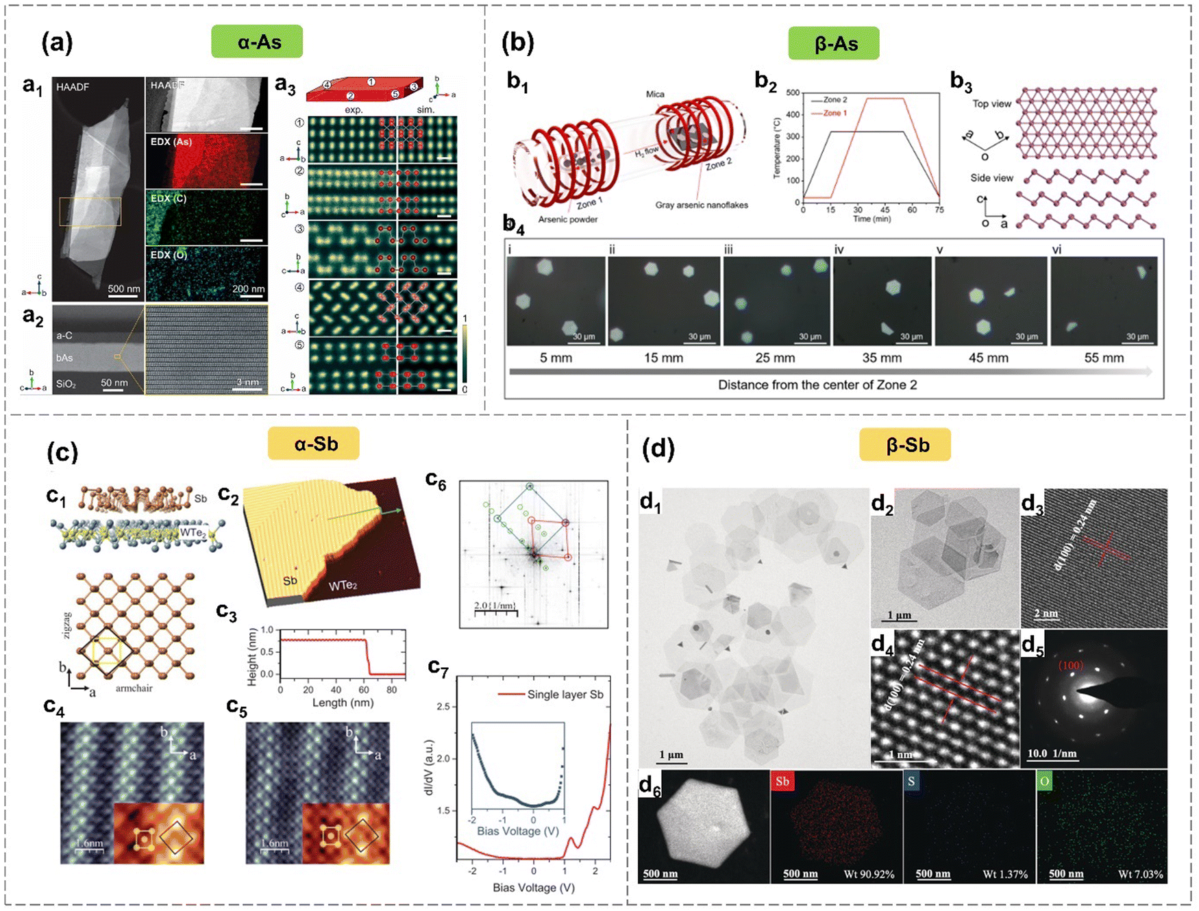 | ||
| Fig. 3 Crystal structures of α-As,32 β-As38 and α-Sb,1 β-Sb.34 (a) α-As prepared by mechanical exfoliation. HAADF-STEM and EDX elemental mapping images of α-As (a1). Cross section of a β-As deposited on SiO2/Si substrate (a2). HAADF-STEM images of β-As from five orientations (a3). (b) β-As synthesized by epitaxial growth on mica substrate. Schematic diagram of epitaxial growth of β-As (b1). Temperature evolution curves of zone 1 and zone 2 during epitaxial growth (b2). Buckled structure of β-As (b3). Optical images of the synthesized β-As (b4). (c) α-Sb epitaxial grown on Td-WTe2 substrate. The puckered honeycomb structure of α-Sb and WTe2 (c1). The STM topology image of monolayer α-Sb on WTe2 (c2) and the height variation along the green line (c3). Atomically resolved STM images taken under U = +300 mV (c4) and U = −50 mV (c5), respectively. FFT image of the STM topology image (c6). STS image of single-layer α-Sb (c7). (d) β-Sb prepared via solution-phase synthesis. LRTEM images of β-Sb nanosheets (d1), (d2). HRTEM images of β-Sb nanosheets corresponding to the (100) plane (d3), (d4). SAED pattern along the [001] axis (d5). HAADF-STEM and EDX elemental mapping images of β-Sb nanosheets (d6). Reproduced with permission from: (a) ref. 32, with permission from American Chemical Society, Copyright 2019; (b) ref. 38, with permission from American Chemical Society, Copyright 2020; (c) ref. 1 with permission from Wiley-VCH, Copyright 2019; (d) ref. 34 with permission from Wiley-VCH, Copyright 2019. | ||
Black arsenene features an orthorhombic lattice similar to BP, characterized by a metastable phase with a space group of Bmab. Its synthesis typically necessitates precise kinetic control. Bulk black arsenic demonstrates semiconductive properties with a direct bandgap of 0.31 eV and exhibits a significant in-plane anisotropy along the armchair and zigzag directions.8 Notably, the properties of ultra-thin arsenene plates frequently diverge from those of bulk materials, highlighting the unique characteristics attainable at reduced dimensions.
Gray and black arsenene exhibit layer-dependent characteristics particularly in terms of their bandgap and dielectric response. For gray arsenene, the bandgap decreases upon increasing the layer number, varying from 0.37 eV (semimetal) of the bilayer to 2.49 eV (semiconductor) of the monolayer.2,55 Precious bandgap values exhibit slight variations depending on different predictive models. As the arsenene number increases from n = 1 to n = 2, black arsenene undergoes a transition from indirect-bandgap semiconductors (1–1.5 eV) to direct-bandgap metallic materials.36,37,61 The dielectric response of black arsenene, as measured by STEM-electron energy loss spectroscopy, shows a correlation with the number of layers.38
Moreover, arsenic and arsenene can undergo a phase transition under specific conditions. For example, bulk arsenic undergoes a phase transition from black arsenic to gray arsenic at a critical pressure of 3.48 GPa, and transfers entirely to gray arsenic above 5.37 GPa. In the case of a few layers, semimetallic gray arsenene nanoflakes (4–48 nm) can be transformed into semiconductive vitreous arsenene nanoflakes through wet chemistry treatment via aqueous hydrofluoric acid (HF) solution.40 Physical and chemical properties of antimonene, including mechanical strength, magnetic properties, electronic and optoelectronic properties, gas sensitivity, and catalytic activity, can be extensively tailored through various engineering methods, i.e., doping,59,62 defect engineering,63–65 heterostructure formation,66,67 chemical absorption68 and stain application.69 For instance, theoretical investigations indicate that the introduction of dopants (Ti, V, Cr and Ni) effectively enhances the interaction between arsenene and hydrogen cyanide (HCN) gas, transforming the adsorption into chemisorption and thereby opening up new avenues for catalytic applications.64
Recent reports reveal that various engineering approaches, such as interface engineering,33,47,71 defect engineering,72,73 doping,74 strain application,75–77 and electron-beam irradiation,78 play a vital role in tailoring the properties of antimonene. Interface engineering has proven effective in tuning the electronic structure of antimonene. For example, narrow-gap semiconducting α-antimonene monolayers are achieved through interface engineering. The specialized three-heights-buckling structural configuration of antimonene, controlled by interfacial interactions with substrate, significantly influences its electronic structure.79 Interlayer strain-induced transitions between indirect and direct bandgaps, achievable through lattice mismatch induced by processes like epitaxial growth, enhance its potential for optoelectronic applications.1 Under pressures exceeding 12%, bandgaps of antimonene decrease significantly, down to 0 eV.29 Additionally, while introducing magnetism in antimonene, defects can impact geometrical symmetry and the band gap. External electric field and strain can easily modify antimonene electronic structure. For instance, Cr-doped antimonene can transform from a magnetic semiconductor to a magnetic semimetal under biaxial tensile strains of 6%.75 Both Cr doping and biaxial compression strains contribute to the visible light absorption efficiency of antimonene.75 Furthermore, electron-beam irradiation can alter the stacking structure of antimonene, with moiré patterns observed in twisted few-layered antimonene.78
2.2 Group 16 Xenes
Chalcogenide atoms, such as selenene (Se) and tellurene (Te), each possess six valence electrons, with configurations of 4s24p4 and 5s25p4, respectively. To achieve a stable octet structure, Se and Te typically form two covalent bonds with their direct neighboring atoms, resulting in 1D-helical chains with a helical turn of 120°, which presents the most stable phase (α-phase). Another stable configuration is the tetragonal phase (β-phase), characterized by a mirror plane and rectangular unit cell, originating from a helix-to-layer transformation of the trigonal monolayer. Additionally, the trilayer rhombic structure with six bonds of the central atom and three bonds of the atoms in the outer layers is called γ-phase (1T-like phase).Based on the transition from the nonmetal sulfur (S) to metal polonium (Po) within group VI, tellurene exhibits more metallic properties. This is due to a stronger delocalization of electrons within the chains of tellurene, leading to covalent-like interactions that are stronger than the van der Waals interactions in selenene. In contrast, based on the calculated cohesive energy, α-Se (3.35 eV per atom) is found to be energetically more stable than α-Te (3.05 eV per atom).80
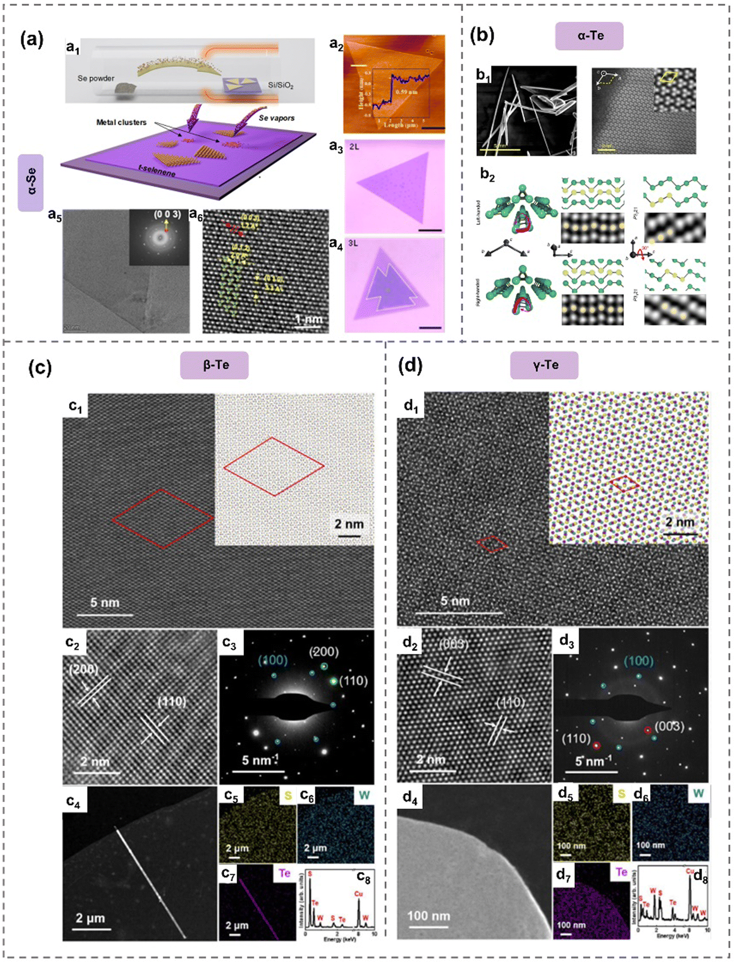 | ||
| Fig. 4 Crystal structure of α-Se48 and α-,87 β- and γ-Te.54 (a) α-Se prepared by seed-assisted CVT. Schematic diagram of CVT process (a1). AFM image of bilayer selenene (a2). Optical images of bilayer selinene (a3) and trilayer selenene (a4). HRTEM image and SAED pattern (inset) of selenene domain (a5). HAADF-STEM image of selinene. (b) α-Te nanowires prepared by hydrothermal method. SEM and STEM of α-Te (b1). Crystal sketches and STEM images of α-Te (b2). (c), (d) Crystal structure of β-Te and γ-Te prepared by vdW epitaxy method on WS2 substrate. β-Te nanosheets (c1) and γ-Te nanoribbons (d1) onWS2. Insets display the β-Te/WS2 (c1) and γ-Te/WS2 (d1) heterostructures. HRTEM image of f β-Te nanosheets (c2) and γ-Te nanoribbons (d2) on WS2. SAED patterns of β-Te/WS2 (c3) and γ-Te/WS2 (d3). TEM images of β-Te nanosheets (c4) and γ-Te nanoribbons (d4). EDS mapping and elemental analysis of α-Te nanosheets (c5)–(c8) and β-Te nanoribbons (d5)–(d8) on WS2. Reproduced from: (a) ref. 48 with permission from Royal Society of Chemistry, Copyright 2022; (b) ref. 87 with permission from Springer Nature, Copyright 2022; (c), (d), ref. 54 with permission from Springer Nature, Copyright 2024. | ||
2D tellurene demonstrates thickness-dependent bandgaps, varying from nearly 0.31 eV for bulk to 1.17 eV for bilayer.92 This material exhibits significantly enhanced optical absorption properties due to a nearly direct or direct band gap and high hole carrier mobility, making it a promising candidate for applications in (opto-) electronics especially the general scarcity of p-type 2D semiconductors.93 Similar to selenene, the properties of tellurene, including the phase transition, bandgap and (opto-) electronic, magnetic, mechanic and catalytic properties, can be optimized through strain,94–99 surface adsorption,100 vacancy,6,100 doping,98 thermal excitations,101 electric fields manipulation102 and heterostructure formation.28,103
Theoretical reports predict several interesting properties of tellurene waiting for experimental validations. First-principles calculations indicate that monolayer tellurene can undergo a β- to α-phase transition under biaxial strains to 0.5%, accompanied by a substantial increase in high piezoelectric coefficient.96 And in-plane compression can facilitate the α- to β-phase transition. And the growth of the tensile strain along the chain direction beyond a critical value, ≈12%, may lead to the α- to γ-phase transition.104 The tellurene bandgap can transition from indirect to direct when the vacancy concentration reaches 5.3%.100
Moreover, transition metal doping and strain engineering can introduce magnetism into α- and β-tellurene while modifying their magnetic moments and electronic properties. Hybrid structures, such as α-Te/h-BN, exhibit enhanced carrier mobility and tunable electronic properties, with boron (B) vacancy driving the transition of Te/BN bilayers from semiconductors to half-metals. Notably, trigonal crystals, including their 2D nanosheets, can be transformed into various metallic structures through reversible metal–semiconductor transitions induced by electrostatic charging.28 Additionally, photoinduced-shear stain in Te films disrupts the screw symmetry of the crystal, contributing to the dynamic band structure.91 Furthermore, tellurium nanofilms exhibit excellent thermoelectric performance, with a room-temperature power factor of 31.7 μW cm−1 K−2 and a ZT value of 0.63.105
2.3 Chemical stability of 2D Xenes
Although arsenene, antimonene, selenene and tellurene are generally stable under ambient environments, it is crucial to consider the influence of oxygen and water during their preparation and storage. Herein, examples of their oxidation and degradation behavior, as well as their advantages and disadvantages in the latest research reports are summarized.The sp3-like hybrid electron structures of As and Sb both have a lone pair of non-bonding electron pairs that can interact with electrons donated by oxygen or water molecules, forming a dative bond.33,38 Specifically, it is observed that the presence of dissolved oxygen in aqueous HF solution significantly accelerates the vitrification process of arsenene nanoflakes (Fig. 5(c) and (d)). This is evident from the significant disparity in the rate of the surface color change of As crystals when exposed to HF in ambient air compared to N2.40 The reaction between As2O3, induced by dissolved oxygen, and HF aqueous plays a crucial role in the formation of As defects/vacancies and unsaturated As atoms, facilitating the transition to the vitreous arsenene.40
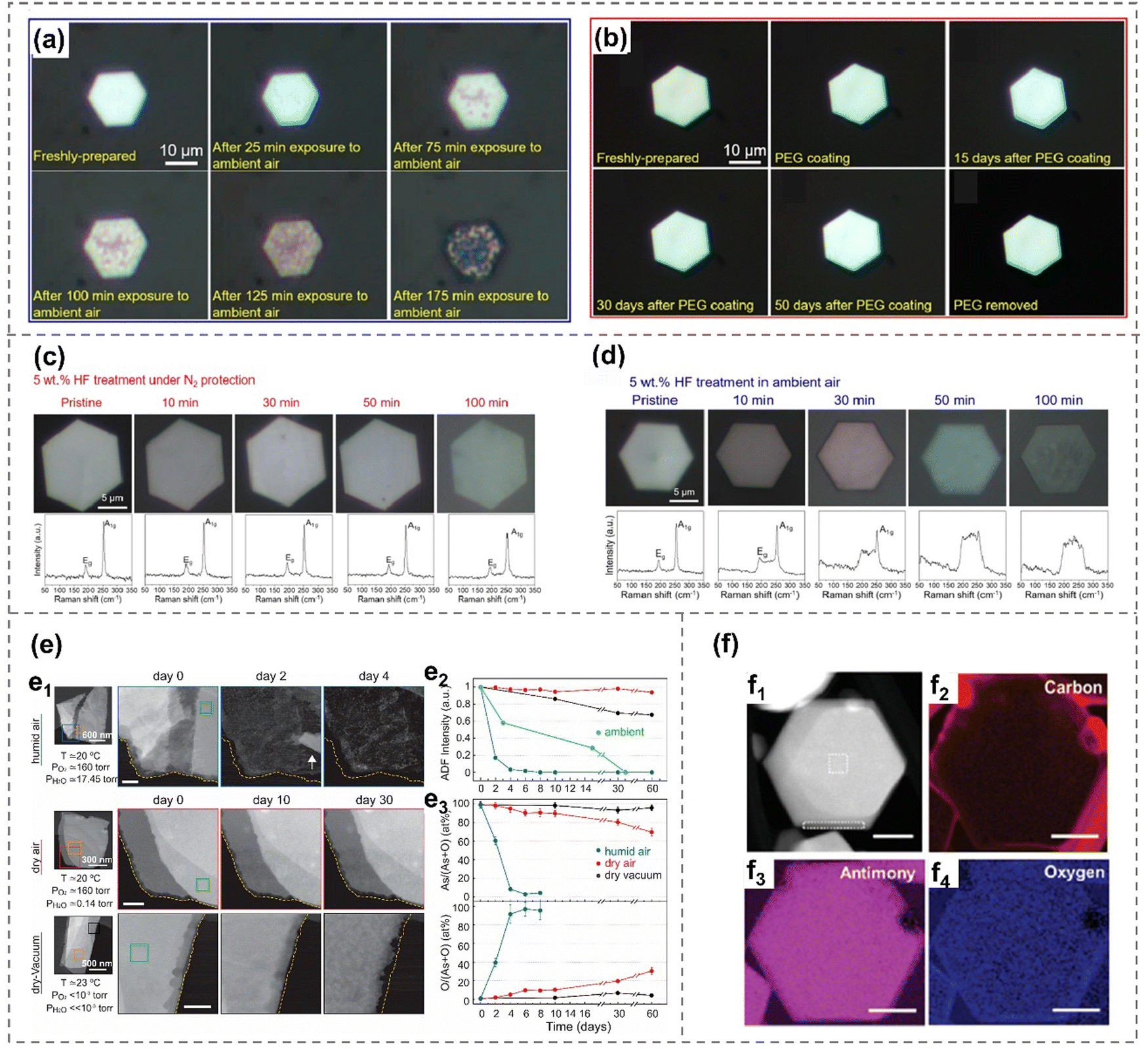 | ||
| Fig. 5 Oxidation and degradation behavior of arsenene and antimonene. (a) Optical images of a β-arsenic nanoflake with varying durations of exposure to the ambient environment.32 (b) An as-prepared β-arsenene nanoflake, followed by its state after PEG coating and removal.32 (c) and (d) Optical images and corresponding Raman spectroscopy of β-arsenene nanoflake after different durations of HF treatment under N2 protection (b) and in ambient air (c), respectively.40 (e) Degradation of exfoliated α-arsenene flakes under humid air, dry air and dry-vacuum environment.38 HADDF-STEM images showing degradation of α-arsenene over time (e1). Changes in HAADF intensity of α-arsenene with time (e2). Elemental composition of α-arsenene over time measured by EDX (e3). (f) HADDF-STEM image (f1) and elemental compositional EELS maps (f2)–(f4) of few-layer antimonene hexagons.106 Reproduced from: (a), (b) ref. 32 with permission from American Chemistry Society, Copyright 2019; (c), (d), ref. 40 with permission from Wiley-VCH, Copyright 2021; (e) ref. 38 with permission from American Chemistry Society, Copyright 2020; (f) ref. 106 with permission from Wiley-VCH, Copyright 2021. | ||
Additionally, the impact of the ambient environment on gray arsenene is directly documented through optical microscopy images (Fig. 5(a) and (b)). Gray arsenic nanoflakes exhibit a transformation from metallic to semiconducting behavior after prolonged exposure to ambient conditions, attributed to the oxidation of arsenic in the air. This also indicates that the control of oxidation degree may be a novel strategy for bandgap modification. The oxidation of arsenic would happen after extended ambient exposure, which can be effectively inhibited by protective coatings that include polyethylene glycol (PEG), polyacrylonitrile (PAN), poly (methyl methacrylate) (PMMA), and polyvinylpyrrolidone (PVP). These protective coatings are employed to safeguard the sample against chemical degradation and phase transition for over 50 days under an ambient environment.32
Besides, the oxygen and water degradation effect of black arsenene is examined via characterization techniques including optical microscopy, Raman, XRD, STEM and EDX spectroscopy.2,38 It shows that black arsenene exhibits a higher resistance to oxidation and vapor in wet air than gray arsenene,21 and the degradation rate of black As is more significant than that in dry air, and the oxygen content of the As flakes increases due to the vanishing of As in wet air. Yun et al. also reported that preventing exposure to water vapor is crucial for protecting black arsenic nanoflakes due to their heightened sensitivity to atmospheric humidity. Consequently, both dry air and a dry vacuum have been shown to be effective methods for safeguarding these nanoflakes.38 In the case of a dry air condition, black As also undergoes an oxygen-increasing process even though there is no reduction of thickness (or As content) and visible degradation, which is due to the formation of an As2O3 protection layer on the surface of black arsenene.38
The oxidation phenomenon of Sb can be detected via the Sb 3d3/2 peak in the unannealed sample, as observed in XPS.33 Additionally, it can also be detected by Raman modes centered at 190 cm−1 and 256 cm−1.100 This phenomenon can be further confirmed by EDX mapping images (Fig. 5(f)).106 However, these oxidation layers can be effectively removed by annealing at 680 K, leading to high-quality antimonate without morphology changes.33,107 In addition to direct contact with chemicals and the ambient environment, electrochemistry can also induce oxidative behavior. For instance, Te can be readily oxidized to TeO2 at merely 0.52 V (versus standard hydrogen electrode, SHE), which hinders its anodic exfoliation and restricts its application to cathodic exfoliation.107
3. Preparation methods
The preparation methods of arsenene, antimonene, selenene and tellurene can be broadly categorized into two primary groups: top-down and bottom-up methods (Fig. 6). Mechanical exfoliation, liquid-phase exfoliation and electrochemical exfoliation are discussed within the scope of top-down strategies, while the bottom-up methods include molecular beam epitaxy, gas-phase deposition methods (including chemical vapor deposition, physical vapor deposition and electrophoretic deposition108) and wet-chemical synthesis (thermal-liquid phase synthesis and thermal assistant techniques).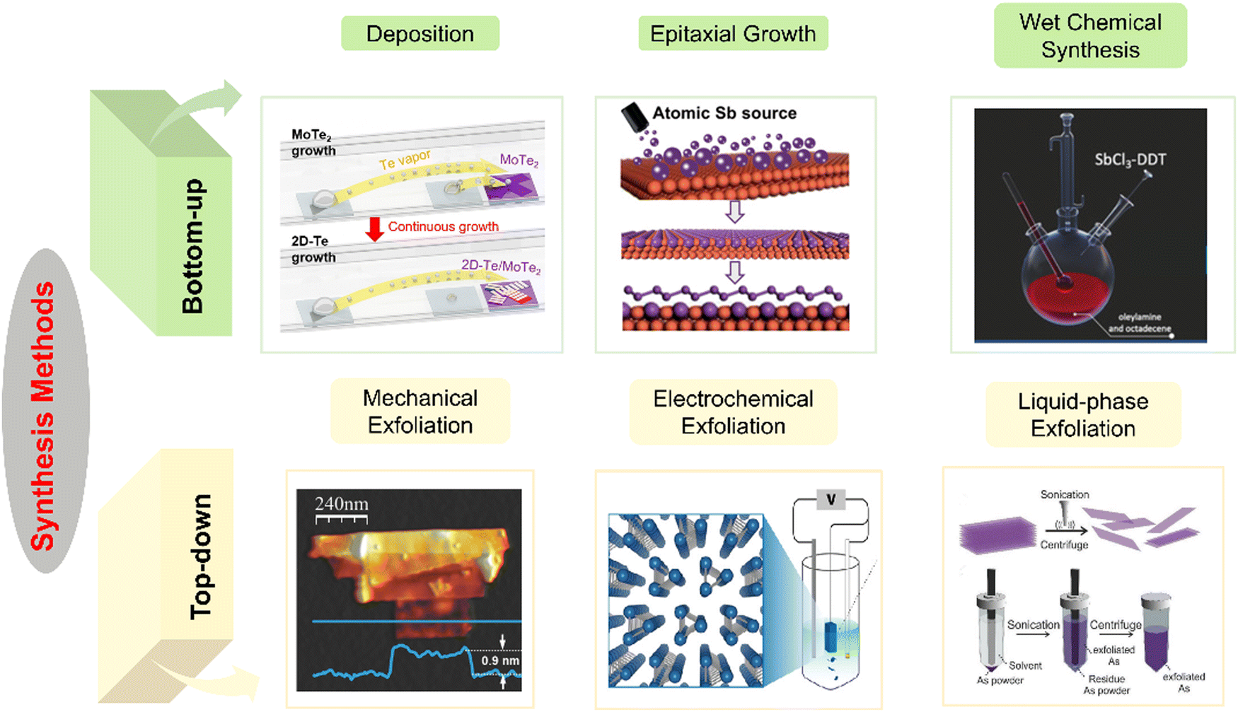 | ||
| Fig. 6 Bottom-up and top-down synthesis methods of antimonene, arsenene, selenene and tellurene. Bottom-up methods include deposition,49 molecular beam epitaxy33 and wet-chemical synthesis.34 Top-down methods include mechanical exfoliation,35 electrochemical exfoliation26 and liquid-phase exfoliation.2 Reproduced with permission from: ref. 49 with permission from American Chemical Society, Copyright 2024; ref. 33 with permission from Wiley-VCH, Copyright 2019; ref. 34 with permission from Wiley-VCH, Copyright 2019; ref. 35 with permission from Wiley-VCH, Copyright 2016; ref. 26 with permission from Wiley-VCH, Copyright 2021; ref. 2 with permission from Wiley-VCH, Copyright 2019. | ||
3.1 Top-down methods
Due to the quasi-2D structure of selenene and tellurene, obtaining single-crystal nanosheets through mechanical exfoliation is challenging. Churchill et al. reported the mechanical exfoliation of trigonal Te single crystals to produce nanoscale Te flakes and wires.108 The silicon substrates require pre-treatment using acetone, isopropanol and O2-plasma to enhance the adhesion of tellurene. The effect of directly sliding a cleaved facet of Te on the substrate is better than the scotch tape method, getting thicknesses of 1–2 nm and widths below 100 nm nanosheets.108 To date, there are no reports on mechanical exfoliation of selenene to our best knowledge, this could be attributed to the scarcity of large, high-quality Se single crystals.108
 | ||
| Fig. 7 (a) Low-potential electrochemical exfoliation.42 Schematic diagram of electrochemical exfoliation of arsenene. The blue ball represents cations (NH4+), while the red ball represents anions (PF6−) (a1). STEM images of sonicated few-layer α-arsenene (a2) and washed and sonicated α-arsenene (a3), (a4). EDX elemental mapping images of As and O element distribution (a5)–(a7). (b) Te crystal prepared by cathodic exfoliation.26 Schematic diagram of Te crystal structure (b1). Electrochemical exfoliation setup and digital photos of the exfoliation process over time (b2). Amperometry curve of the exfoliation over time with a potential of −1.36 V vs. Hg/HgO (b3). UV-vis spectroscopy of the exfoliated Te nanosheets before and after O2 purge (b4). Optical (b5) and AFM images (b6), (b7) of Te on the Si/SiO2 substrate. Reproduced from: (a) ref. 42 with permission from American Chemical Society, Copyright 2020; (b) ref. 26 with permission from Wiley-VCH, Copyright 2021. | ||
Zheng et al. employed a cathodic exfoliation method to exfoliate tellurium crystals into Te nanosheets, achieved at an overpotential of approximately −0.4 V versus the reversible hydrogen electrode (RHE) in an alkaline solution (1.0 M KOH).26 The reduction of Te0 atoms at both the edge and plane regions to Te22− facilitates the insertion of K+ ions between the interlayers or interchains of Te, ultimately forming KTe2−. The KTe2− flakes with negative charge exhibit mutual repulsion, ensuring stability in solvent for 10 hours. These Te nanosheets can be collected with the assistance of dissolved oxygen, which prompts the conversion of Te22− back to Te0. This electrochemical exfoliation method can contribute to the doping of metal in the active site, promoting the hydrogen evolution reaction (HER) activity of the materials.26 Han et al. prepared high-quality antimonene nanosheets through an electrochemical lithiation intercalation process, followed by ultrasonication.44 These Sb nanosheets serve as effective heterogeneous nucleation sites to promote the preferential growth of perovskite films.44
Additionally, N-methylpyrrolidone (NMP) has emerged as the preferred solvent, offering the highest concentration of stable arsenene sheets. Notably, the crystalline structure of arsenene, whether in zigzag or armchair directions, remains well-preserved during the LPE process (Fig. 8(a)). The exfoliated sample with a thickness of 5–12 nm is stable, although slight oxidation occurred, demonstrating the versatility of employing solvents with diverse boiling points and surface tensions for the exfoliation of arsenene. Exfoliated few-layer arsenene demonstrates promise in applications as gas sensors, which can selectively detect either methanol or acetone vapors depending on the chosen frequency.2
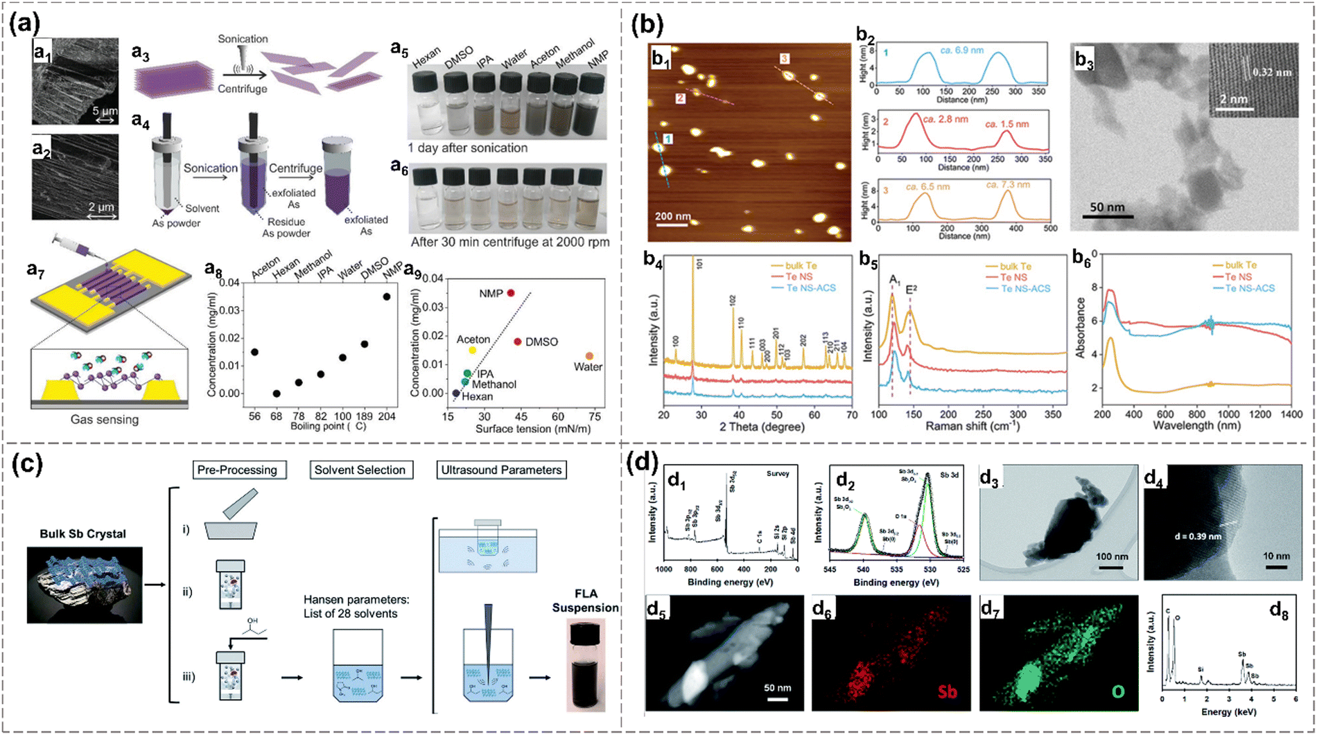 | ||
| Fig. 8 Liquid-phase exfoliation methods. (a) Arsenene prepared by liquid-phase exfoliation and tip ultrasonication in different solvents.2 SEM images of a layered bulk arsenic (a1), (a2). Schematic diagram of the tip ultrasonication and centrifugation process (a3), (a4). Digital photos of arsenene dispersed in different solvents after ultrasonication (a5) and after centrifugation (a6). Schematic diagram of vapor sensing setup based on prepared arsenene (a7). Arsenene concentration in various solvents with different corresponding boiling point (a8) and surface tension (a9) after 2000 rpm centrifugation. (b) Atomic cobalt species functionalized Te nanosheets (Te NS-ACS) prepared by liquid-phase exfoliation chemical functionalization.27 AFM image (b1), thickness distribution (b2), TEM and HRTEM images (b3) of Te NS-ACS. XRD pattern, Raman spectroscopy and UV-vis absorption spectroscopy of bulk Te, Te NS and Te NS-ACS. (c) Optimization strategies of liquid phase exfoliation. Pre-processing is (i) griding, (ii) dry ball-milling, (iii) wet ball-milling bulk Sb.112 Solvent selection based on Hansen parameters using 28 different solvents (iii). Ultrasonication parameters comparison of bath and tip sonication. Method (iii) exhibits the optimum route to obtain FL Sb with the highest concentration. (d) FL-Sb nanosheets obtained by exfoliation using ball-milling and ultrasonication.45 XPS (d1), Sb 3d spectrum (d2), TEM (d3), HRTEM (d4), HAADF-STEM (d5), EDX elemental mapping (d6), (d7), EDX spectrum (d8) of FL-Sb flakes. Reproduced from: (a) ref. 2 with permission from Wiley-VCH, Copyright XXXX; (b) ref. 27 with permission from Wiley-VCH, Copyright 2020. (c) ref. 112 with permission from Royal Chemistry of Society, Copyright 2019; (d) ref. 45 with permission from Royal Chemistry of Society, Copyright 2020. | ||
In the case of antimonene, the impact of initial crystal size, solvent selection and ultrasound parameters on liquid-phase exfoliation is explored. Wet-ball milling with 2-butanol, coupled with tip sonication yields superior results compared to bath sonication.70 Additionally, a few-layer antimonene is prepared by a combination of ball milling and sonication-based liquid exfoliation in a 4:1 isopropanol/water mixture using Sb bulk crystals. The EDX spectroscopy shows the existence of oxygen on the prepared Sb nanosheets, which is consistent with XPS results (Fig. 8(d)).45 Gibaja et al. applied standard LPE with three different preprocessing methods: grinding the bulk Sb crystal, dry ball-milling, and wet ball-milling (Fig. 8(c)). These methods do not have a significant impact on the in-plane structure, crystal phase, or composition of the exfoliated antimonene. The wet ball-milled samples exhibit the highest concentration.112 Similarly, 2D tellurene is successfully exfoliated by LPE.27,116 Tellurene nanosheets (NS, 2-8.2 thickness) are exfoliated using the bulk tellurene in NMP solution via an ultrasonication device. The as-exfoliated samples react with CoCl2·6H2O to get the Te NS-ACS (atomic cobalt species), which is indicated by XRD, Raman and UV-vis absorption spectra (Fig. 8(b)).27
3.2 Bottom-up methods
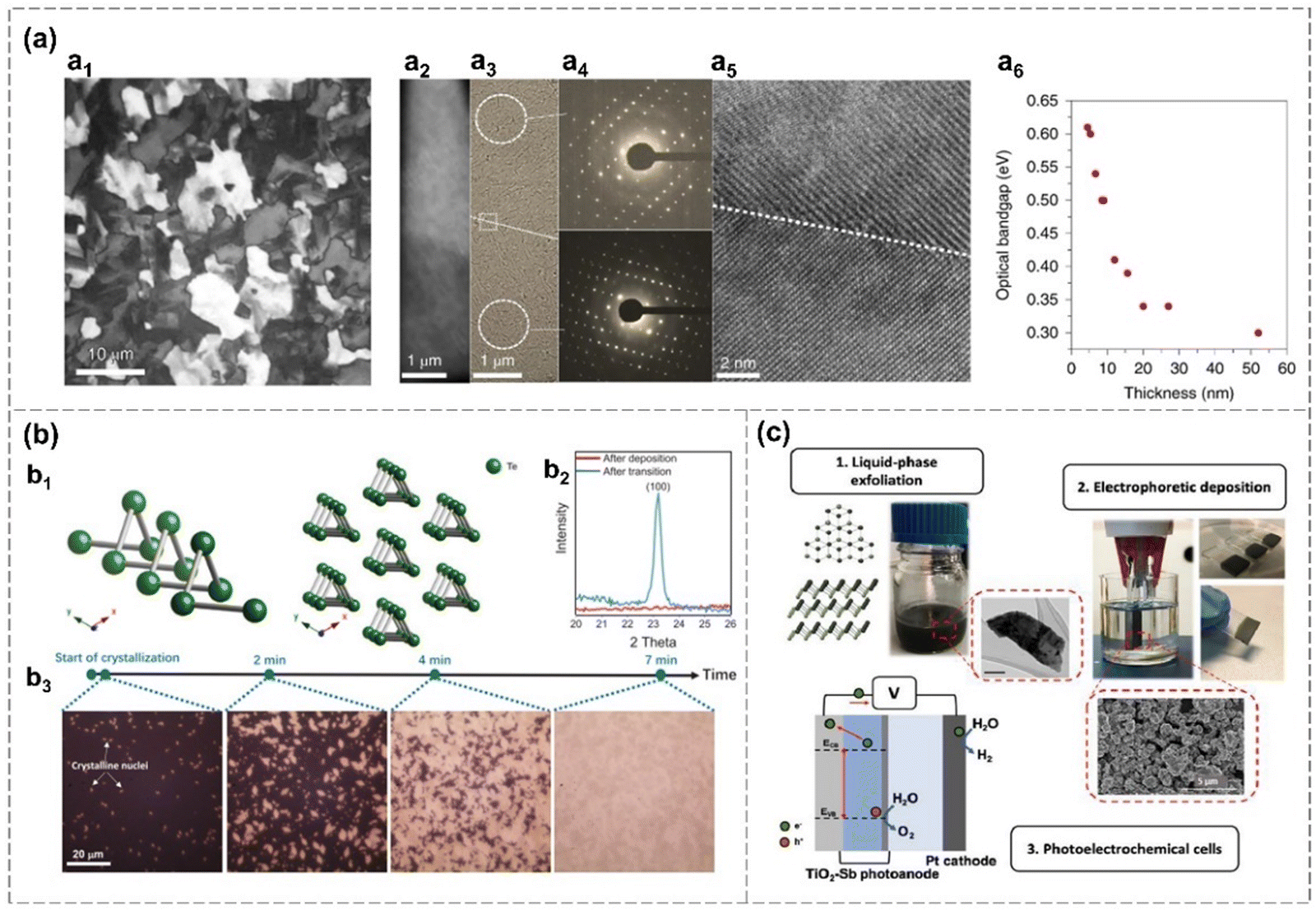 | ||
| Fig. 9 Deposition methods. (a) Evaporated Te thin films on a −80 °C substrate.51 Polarized light microscopy of a Te film (a1). Optical image of a Te film on SiO2 TEM grid, showing a grain boundary (a2). TEM images of a Te film (a3) and corresponding SAED pattern (a4). HRTEM image of the same film and the grain boundary (a5). Optical bandgap changes over the thickness of a Te film. (b) Phase transition of evaporated Te films.89 Te crystal structure (b1). XRD pattern of a Te film (50 nm) evaporated on the SiO2/p+-Si substrate (−80 °C) after deposition and crystallization (b2). Optical microscopy images of the crystallization process for an as-deposited 10 nm-thickness Te film (b3) at room temperature. (c) Electrophoretic deposition (EPD) of liquid-phase exfoliated antimonene on conductive substrates and its activity as a light absorber and hole acceptor layer in photoelectrochemical cells (PECs).43 Reproduced from: (a) ref. 51 with permission from Springer Nature, Copyright 2020; (b) ref. 89 with permission from Royal Chemistry of Society, Copyright 20201; (c) ref. 43 with permission from Elsevier, Copyright 2020. | ||
Zhao et al. revealed that the grain size and orientation of the evaporated films can be finely controlled through crystallization processes on cold SiO2/Si substrate (−80 °C).89 As-deposited Te film is amorphous and the transformation from amorphous to crystalline is shown in Fig. 9(b). New crystalline nuclei appear within the non-transformed portions of the sample throughout the transformation process. Eventually, the entire film undergoes a transformation into a polycrystalline structure, which is confirmed by the occurrence of the (100) peak from the XRD measurement (Fig. 9(b)).89 The crystal growth kinetics related to nucleation rate, nucleus free energy, interface free energy and temperature is explained theoretically.89 Highly crystalline tellurium (Te) nanosheets, featuring well-defined shapes and sharp edges, are successfully synthesized through CVD.117 The growth mechanism is governed by surface energy considerations, with [001] and [100] orientations experiencing faster growth rates compared to other directions. These Te nanosheets demonstrate impressive capabilities in blackbody-sensitive infrared detection, exhibiting exceptional blackbody and polarization responses.117 Hydrogen is applied to reduce TeO2 to synthesized Te nanosheets, with H2O formation promoting the formation of Te flakes.90 Te nanosheets are also successfully prepared via continuous template growth on 1T′-MoTe2via CVD.49
A seed-assisted CVT growth is employed to produce ultra-thin, highly-crystalline α-Se nanosheets with a triangle-shape.48 These nanosheets are oriented in (0001) direction and exhibit lateral dimensions exceeding 30 μm with an ultralow thickness of 0.59 nm (Fig. 4(a)). Sb, Bi and Sn are employed as seeding metals for the growth of α-Se. α-Se growth mechanism involves two steps: the initial formation of 3D selenium islands followed by lateral growth into a triangular shape. The nano-islands formed at both the edges and interiors during the initial growth phase are subsequently driven toward the edges of the domains with the progression of domain growth. The introduction of hydrogen atoms, serving as passivation agents for terminal Se atoms, proves instrumental in stabilizing the lattice of α-Se nanoflakes.48 α-Se flakes are reported to grow directly on the c-axis of the sapphire substrate via physical vapor deposition (PVD), contributing to the fabrication of α-Se based Schottky barrier diodes (SBDs).82 And hydrogen-assistant PVD is also utilized in the synthesis of tellurene. The introduction of hydrogen enhances the vapor pressure within the system and induces the reduction of TeO2, ultimately facilitating the formation of tellurene.48 Additionally, as shown in Fig. 9(c), the LPE-prepared β-antimonene film can also deposited on various substrates, such as a TiO2 coated fluorine-doped tin oxide (FTO) electrode, through electrophoretic deposition, exhibiting good optical absorption and charge separation ability in the photoelectrochemical cell (PEC).
The synthesis of arsenene using the CVD technique faces certain limitations due to the vitality and thermal stability of the arsenic precursors. However, in industrial processes, arsenic precursors such as hydrides and alkyl/aryl hydrides are broadly employed due to their low thermal decomposition properties. This allows for the design of a suitable substrate for the future deposition of arsenene in large areas.118
For instance, β-antimonene monolayers are successfully prepared on PdTe2 substrates, which have a small lattice mismatch with that of free-standing Sb and high chemical stability.107 Multilayer antimonene nanoribbon-like flakes, crystallizing in the β-phase and extending over several microns in length, are realized through molecular beam epitaxy (MBE) and subsequent in situ thermal annealing on sapphire substrates.119 The formation mechanism may be attributed to the transition of thermodynamic shape, enabled by the enhanced adatom mobility at elevated annealing temperatures.119 Shi et al. reported the successful large-scale synthesis of monolayer α-antimonene via MBE, employing Td-WTe2 as the substrate because of its surface chemical inertness and lattice matching with α-Sb.1 A monolayer growth mode is initially favored, characterized by the formation of defect-free Sb islands with no detectable defects, and no phase transition during growth is detected.1 Besides, single-crystalline β-antimonene is prepared by MBE on Cu (111) and Cu (110), respectively (Fig. 10(a) and (b)).33 The antimony is evaporated under 640 K, and deposited on the copper surface at room temperature, forming twofold symmetry Cu–Sb surface alloy and threefold symmetric antimonene. The lattice mismatch between the epitaxial substrates and 2D antimony coverage can introduce compressive or tensile strain, contributing to various bandgaps of antimonene.33 Additionally, an antimonene monolayer with a three-height-buckling configuration overlaid on a SbAg2 surface alloy-covered Ag (111) substrate is synthesized by molecular beam epitaxy.79
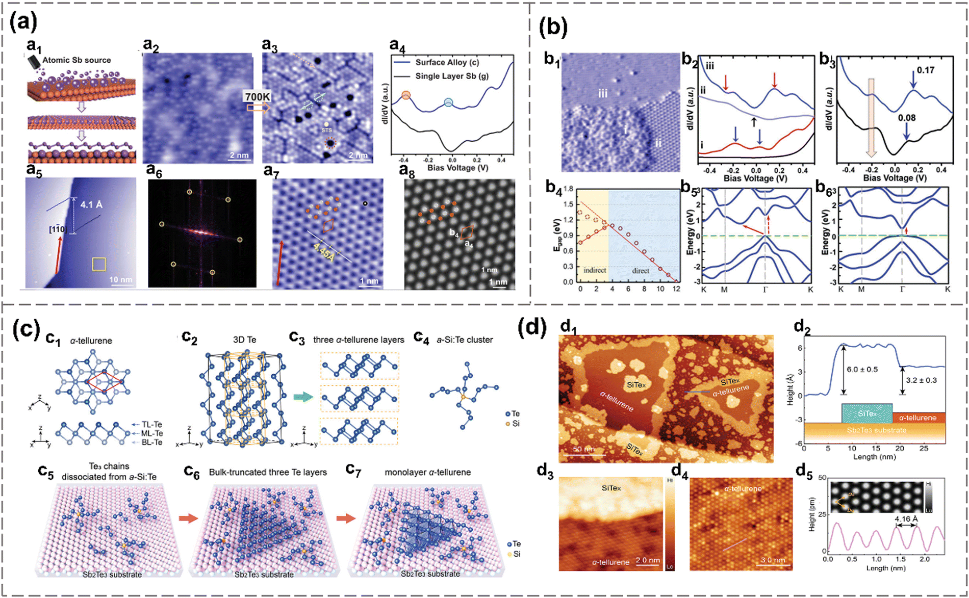 | ||
| Fig. 10 Molecular beam epitaxial. (a) Crystal structure and electronic property of antimonene on Cu (111).33 Schematic diagram of MBE process: dispersed Sb atoms, alloy with substrate and as-prepared antimonene (a1). STM topographic image of 0.5 monolayer Sb on Cu (111) before annealing (a2) and after annealing (a3). STS of surface alloy and single layer Sb (a4). STM image of well-ordered monolayer antimonene on Cu (111) after annealing at 700 K (a5) and corresponding FFT (a6). High-resolution STM image of antimonene taken from the yellow zone in a5 (a7). Simulated STM image of antimonene (a8). (b) Electronic structure of antimonene grown on Cu3O2/Cu(111).29 Grain boundary of antimonene.88 (i) clusters, (ii) Sb pattern and (iii) antimonene (b1). STS spectra of bare Cu3O2/Cu(111) and three phases as illustrated in b1 (b2). STS spectra of antimonene on Sb–Cu (111) alloy surface (b3). Bandgaps of free-standing Sb under tensile strain calculated by DFT (b4). Band structures of free-standing Sb (lattice constant is 4.01 Å) (b5) and Sb on Cu3O2/Cu(111) (where lattice constant of Sb is 4.35 Å) (b6). (c) Synthesis of γ-Te.88 Schematic diagram of γ-Te monolayer (c1), 3D Te chains (c2), tri-layer Te (c3), Te-rich a-Si: Te cluster (c4). Epitaxial growth steps of Te on Sb2Te3 substrate (c5)–(c7). (d) Morphology of Te grown on a Sb2Te3 substrate.88 STM topographic image of γ-Te grown on Sb2Te3 (d1). Edge-step between γ-Te and SiTex (d2). Atomic-resolution STM image of γ-Te (d3). Height along the pink line in d3 (d4). Height along the blue line in d1 (d5). Reproduced from: (a) ref. 33 with permission from Wiley-VCH, Copyright 2019; (b) ref. 29 with permission from Wiley-VCH, Copyright 2020; (c), (d), ref. 88 with permission from Wiley-VCH, Copyright 2024. | ||
Besides metallic substrates, antimonene can also be epitaxially grown on dielectric substrates such as copper oxide through the MBE segregation process, which ranges from Sb dimer chains and hexagonally packed dot arrays. Eventually, Sb spreads over the surface and forms monolayer antimonene. There is a weak van der Waals force formation (as indicated by electronic localization function) between Cu3O2/Cu(111) and antimonene, preserving its semiconductor property (direct bandgap, 0.37 eV).29
Additionally, MBE is employed to cultivate high-performance optoelectronic nanodevices. Kang et al. synthesized 2D single-crystalline Te nanobelts on SrTiO3 (001) substrates. This synthesis involves a preliminary substrate treatment consisting of combined chemical etching and thermal annealing. The process culminates in nanobelts that exhibit impressive photoconductive performance, including a broad spectral response range from the near-ultraviolet to the near-infrared regions, along with rapid response and decay times of 510 μs and 300 μs, respectively.50
Moreover, a self-assembly approach, using α-Si: Te alloy as building blocks, is employed to grow γ-phase monolayer tellurene on a Sb2Te3 substrate epitaxially. First, twofold coordinated Te chains are linked together by fourfold coordinated Si atoms to form an alloy (Fig. 10(c) and (d)). Then, under high temperatures, the structure of the alloy softens, and the twofold coordinated Te can dissociate from the alloy and form Te3 chains on the substrate in the continuous Te flux. And the Te3 chains will self-assemble into a hexagonal lattice.88
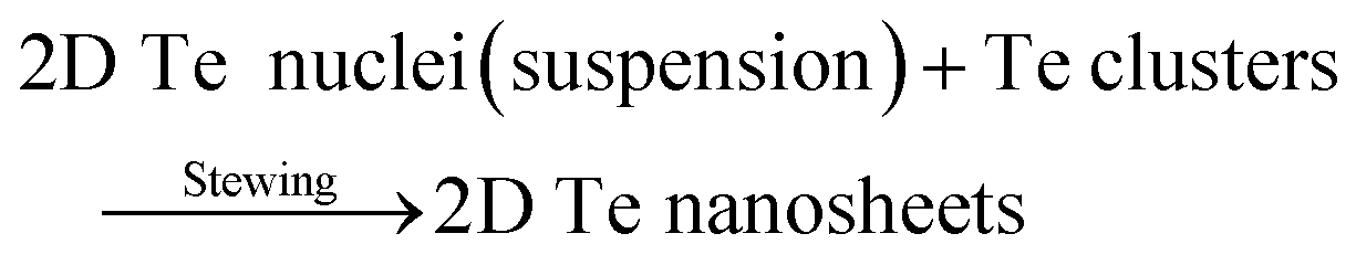
In 2019, few-layer β-antimonene with a hexagonal structure was successfully synthesized using SbCl3 solutions as the source and oleylamine as the reducing agent, promoting their anisotropic growth in a colloidal solution (Fig. 11(a)). EDS reveals a small amount of S and O in the prepared gray Sb source from the precursor and surface oxidation, respectively. Dodecylthiol (DDT) and halide ions are identified as key contributors to avoiding the precursor transfer to Sb2O3 and to the formation of a few-layer antimonene, respectively (Fig. 11(a)).34 The air-stable 2D tellurene, ranging from a monolayer to tens of nanometres, is successfully prepared via a hydrothermal method conducted in a high-pressure autoclave, with PVP and Na2TeO3 as precursors, and deionized water as the solvent. Controlling PVP concentration is the key to obtaining 2D tellurene, and the growth outcomes for different PVP concentrates with varying times of reaction are shown in Fig. 11(b). The synthesized Te nanoflakes display remarkable optoelectronic performance, including high hole mobilities up to 458 cm2 V−1·s−1 under ambient conditions, exceptional anisotropic behavior and a broad bandwidth under 1.55 μm communication wavelength.120 Another study achieves the synthesis of Te nanoflakes with a trigonal phase via hydrothermal methods. Due to shared identical growth directions between two nanoflakes, the nearly symmetrical morphologies are formed, including “V-shapes”, “paper airplane-shapes” and “heart-shapes” (Fig. 11(d)).121 The growth mechanism of 2D Te nanosheets is explained based on experimental evidence. Intersecting nanowires grow along respective 〈0001〉 direction initially, and then the growth direction is well-controlled using the passivation effect of PVP, leading to a transition from 1D nanowires to quasi-2D symmetrical nanoflakes.121
 | (1) |
 | (2) |
 | (3) |
 | (4) |
 | ||
| Fig. 11 Wet-chemical synthesis of antimonene and tellurene. (a) Schematic diagram of the wet-chemical synthesis of hexagonal antimonene, antimony trioxide and antimony tetrahedral.34 (b) Solution growth and process of tellurene.120 Productivity of tellurene over reaction time with different PVP concentrations (b1). Morphology evolution from Te nanowires to 2D tellurene over growth time (b2). Thickness and width of Te over mole ratios (Na2TeO3/PVP) (b3). The thickness of 2D tellurene over a reaction time of thinning (b4). (c) Characterization of 2D antimonene prepared by colloidal approach.106 XPS spectra of Sb and S under different reaction conditions (c1). TEM image of antimonene prepared at ambient temperature and t = 0 h (c2). Sb particles obtained after t = 2 h (c3) and t = 48 h (c4).106 (d) Synthesis mechanism of symmetric Te nanoflakes.121 TEM images of the “V-shaped” Te nanoflake (d1), “heart-shaped” Te nanoflake (d2) and “paper airplane-shaped” Te nanoflake (d3). Illustration of morphology evolution from Te nanowire to symmetrical Te nanoflake (d4). Reproduced from: (a) ref. 34 with permission from Wiley-VCH, Copyright 2019; (b) ref. 120 with permission from Springer Nature, Copyright 2018; (c) ref. 106 with permission from Wiley-VCH, Copyright 2021; (d) ref. 121 with permission from Wiley-VCH, Copyright 2021. | ||
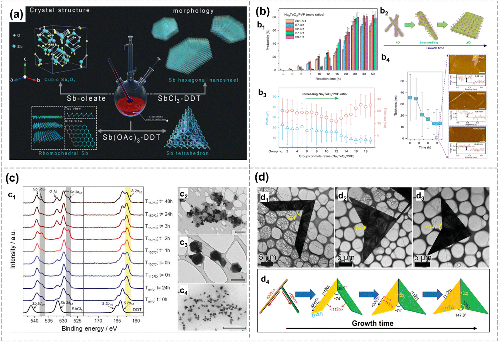
Notably, Qi et al. developed a novel ultrasonication-assisted synthesis method for the successful preparation of tellurene.9 As shown in Fig. 12, 1T′-phase MoTe2 is applied as a Te source as well as the 2D growth template of 2D tellurene, eliminating the requirement for ligands or surfactants and ensuring environmental friendliness. The proposed synthesis mechanism is depicted in formula (1)–(4). 1T′-MoTe2 initially undergoes an ultrasonication treatment in NMP solvent, which facilitates the delamination of van der Waals crystal. Then, a mild ultrasonication process is applied to disperse the mixture and generate the stable suspension of 2D tellurium nanosheets. The synthesis mechanism involves multiple interactions between energy and materials, encompassing crystal exfoliation, atomic escaping from the 2D lattice, preferential nucleation on 2D templates, and guided crystal growth. The resultant tellurene nanosheets exhibit single crystallinity with well-defined morphology and clean surfaces. 2D tellurium-based transistors demonstrate outstanding electrical performance, characterized by exceptional hole mobilities exceeding 1000 cm2 V−1 s−1, and remarkable stability in both solid-state and liquid configurations.
 | ||
| Fig. 12 Template growth of tellurene.9 (a), (b) Schematic diagram of tellurene synthesis using metastable 1T′ MoTe2 as the growth template (a) and corresponding proposed mechanism (b). (c) Characterization and growth mechanism of 2D Te. Optical microscopy of synthesized 2D tellurene (c1). AFM image of a 2D tellurene with a thickness of 10 nm (c2). HAADF-STEM images of 1T′ MoTe2 along 〈103〉 (c3) and 〈100〉 (c4) axis. XPS spectra of Mo 3d (c5) and Te 3d (c6) of 1T′ MoTe2. HRTEM image of 1T′ MoTe2 after ultrasonication. Red circles indicate the existence of defects (c7). HRTEM image of polycrystalline MoO2 on the surface of 1T′ MoTe2(c8). XPS spectra of Mo 3d (c9) and Te 3d (c10) of exfoliated 1T′ MoTe2. XRD pattern of pristine and exfoliated 1T′ MoTe2. UV-vis absorption spectra of the suspension 1T′ MoTe2/NMP (c12) and bulk Te/NMP (c13). Reproduced from ref. 9 with permission from Wiley-VCH, Copyright 2023. | ||
4. Application of Xenes in catalysis
Antimonene has emerged as one of the most extensively studied Xenes for catalytic applications, closely followed by tellurene. Although pure Xenes generally possess limited catalytic activity due to their electron-enriched structure, which hinders the effective splitting of the molecule,16 Xenes can serve as promising substrates for atom loading to achieve enhanced catalytic performance. Furthermore, various engineering strategies, including the construction of van der Waals heterojunctions, the introduction of vacancies, interlayer modification, etc., are employed to amplify the catalytic potential of Xenes.Besides experimental studies, an increasing number of theoretical calculations are being used to predict the catalytic performance of Xenes and their composite materials. For example, a learning classifier utilizing synthetic minority oversampling technology (SMOTE) is developed to identify 140 modified materials with promising HER properties from a pool of 25 low-cost transition metal and 2 nonmetal heteroatom dopants, all incorporated into gray arsenene systems. This selection is based on the principle of Gibbs free energy changes (DGH), which are less than 0.2 eV.60 Subsequently, 13 types of Fe-single-atom-doped arsenene were developed as cost-effective catalysts following the principle of simple laboratory synthesis. This advanced machine learning approach addresses the inefficiencies of traditional high-throughput calculations and has demonstrated remarkable accuracy in predicting outcomes within complex systems. This work holds great promise for reducing labor costs and achieving efficient screening of the Xene catalyst systems. In this section, the discussion on the catalytic application of Xenes will be divided into electrocatalysis and photocatalysis.
4.1 Electrocatalysis
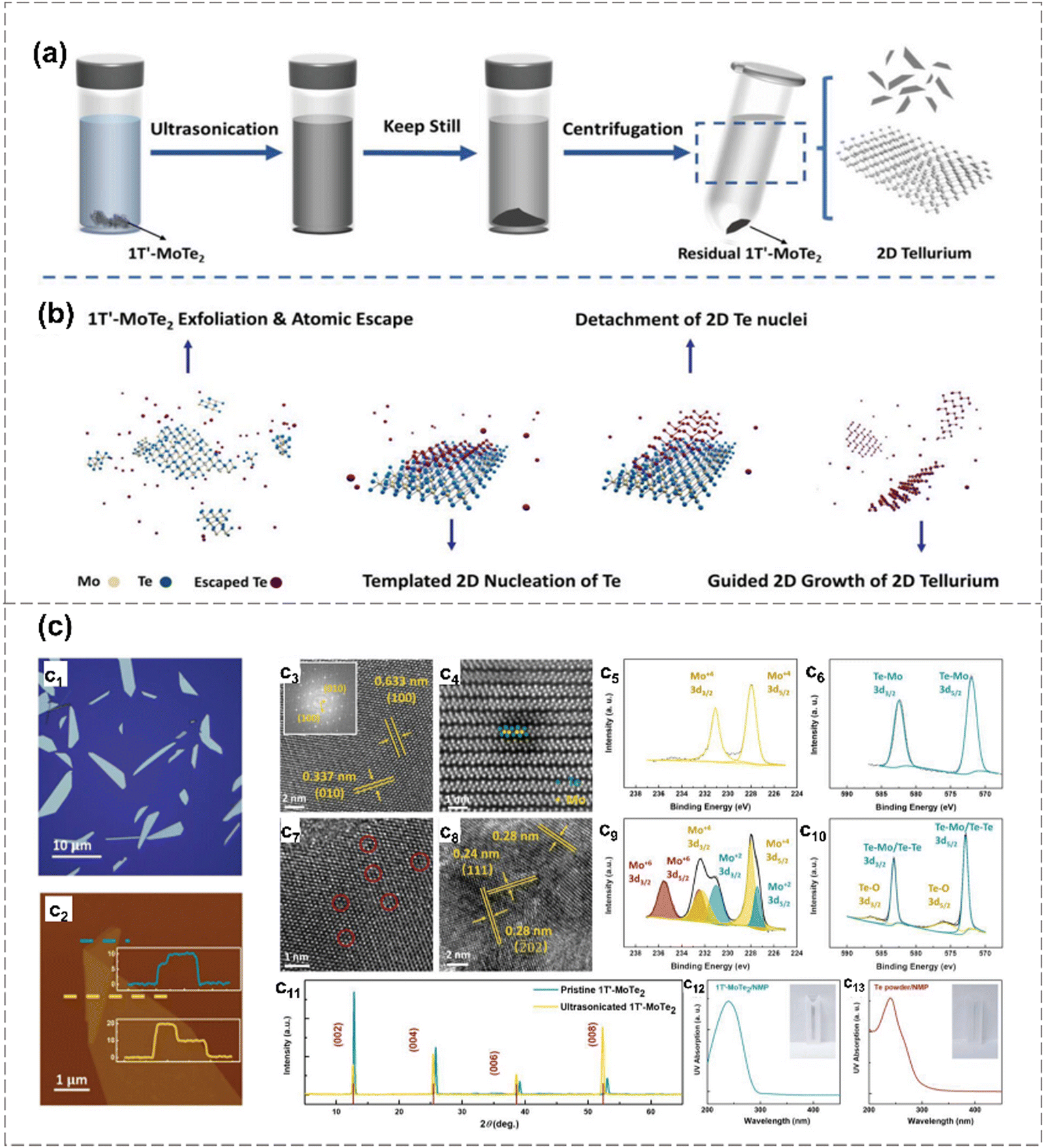
Wu et al. investigated the electrostatic gating, electrocatalytic properties, and electrochemical stability of tellurene across various electrolyte systems.39 Tellurene synthesized via hydrothermal (h-Te) and chemical vapor deposition (c-Te) methods exhibits layer-dependent ambipolar transport properties, with notable high hole mobility and stability in both aqueous electrolytes and ionic liquids. Furthermore, the electrochemical performance of tellurene is investigated using the emerging on-chip electrocatalytic microdevices (OCEMs), which enable the detection of catalytic performance at the level of single nanosheets (Fig. 13(a)). In this study, AgCl/Ag serves as the reference electrode (RE), and the electrochemical potential is referenced to the reversible hydrogen electrode (RHE), as described by the following equation:| ERHE = EAg/AgCl + 0.219 V | (5) |
 | ||
| Fig. 13 (a) Electrocatalytic HER of α-phase tellurene investigated via OCEMs.39 Schematic diagram of an OCEM for in situ transport measurements of tellurene (a1). Optical microscopy image of h-Te devices with exposure area for testing (a2). Polarization curves of h-Te (black) and c-Te (red) (a3). Tafel plots of h-Te (black) and c-Te (red) obtained from a3 (a4). (b) Electrochemical stability of h-Te HER polarization curve and in situ transport property of h-Te in 0.5 mol L−1 H2SO4 at Vds = 100 mV (b1). Optical image and Raman mapping of the h-Te device after the chemical test (b2). Electrochemical curve (red) and transport curve (black) in the oxidation zone (b3). Optical images of the h-Te device before and after the test (b4). Reproduced from ref. 39 with permission from Wiley, Copyright 2023. | ||
Pristine α-phase tellurene is found to demonstrate excellent HER activity in acidic electrolytes, as indicated by its low Tafel slopes and high electrochemical stability across a wide potential window (Fig. 13). Such remarkable performance is attributed to the presence of vacancies, which act as active sites. Specifically, α-phase tellurene synthesized via the hydrothermal method exhibits an overpotential of 435 mV and a Tafel slope of 53 mV dec−1. Moreover, few-layer antimonene is obtained via liquid exfoliation and employed as a non-metal bi-functional electrocatalyst for whole water splitting. It exhibits good catalytic activity and long-term stability in both OER and HER in an alkaline KOH solution.122 The lowest Tafel slope of few-layer Sb nanosheets is 261.3 mV dec−1 for OER and 217.2 mV dec−1 for HER.122
Furthermore, in 2019, Lloret et al. reported the application of pristine Xenes in catalyzing organic reactions.123 Few-layer, high-crystalline 2D Sb and BP with minimal defects in the zero-oxidation state are prepared by LPE using 1-butyl-3methylimidazolium tetrafluoroborate (bmim-BF4). These materials act as efficient catalysts for the alkylation of nucleophiles (such as alcohols, thiols and indoles) with simple esters under mild chemical environments. The use of Bmim-BF4 and a glove box prevents oxidation and moisture-related degradation during the fabrication process, thereby ensuring the stability of antimonene. This research offers a more accessible alternative mechanism to the harsh reaction conditions typically associated with superacid-catalyzed alkylation with esters. Notably, 2D antimonene outperforms BP due to its higher polarization effect, which enables the selective alkylation of acid-sensitive aromatic derivatives with simple esters. Additionally, a theoretical study suggests that the β-arsenene monolayer could exhibit an ultralow thermodynamic overpotential of 0.068 V for the anodic chlorine evolution reaction (CER).124 The formation of antimony oxides on the surface can enhance its catalytic performance. To be specific, 2D Sb nanoflakes are used as an efficient electrocatalyst for the nitrogen reduction reaction (NRR), with a high NH3 production rate of 180.4 μg h−1 mgCAT−1 and 11.6% faradaic efficiency (FE) in 0.1 M KOH solution under ambient environments. The theoretical calculations indicate that the oxidized species of antimonene serve as the active catalytic sites during the NRR process, and the increasing polarity resulting from facial oxidation makes the absorption energy of N2 more favorable.45
Additionally, antimonene is applied as a cocatalyst substrate and loaded with Pt atoms through the intercalation and reduction facilitated by ethylenediamine (EDA).114 The presence of Sb as the cocatalyst alters the oxidation pathway of formic acid on the Pt catalyst, favoring the dehydrogenation pathway reaction.114 A computational study indicates that Pt supported on an Sb substrate can be effectively activated to lower oxidative states, promoting the electrooxidation of HCOOH and reducing the CO poisoning effect. The as-prepared Pt/Sb exhibits a 4.5-fold increase in specific activity for the formic acid oxidation reaction (FAOR), and 2.6-fold higher mass activity compared to the conventional Pt/C catalysts.114 Antimonene has also been employed as a support for RuS2 nanoparticles, forming Ru–S–Sb bonds.71 The RuS2 nanoparticles exhibit in situ growth on sonication-exfoliated Sb nanosheets, demonstrating more stable catalytic abilities than Pt/C even after 40 hours of operation. The Ru–S–Sb/Sb heterostructure achieves a faradaic efficiency of 100% and displays low Tafel slopes and high current density in both acidic (0.5 M H2SO4) and alkaline (1.0 M KOH) electrolytes. DFT calculations reveal that the formation of Ru–S–S promotes charge density around Ru–H, facilitating hydrogen absorption and reducing the HER thermodynamic barrier on the RuS2 surface.71
Doping and defect engineering are the two most widely reported strategies for optimizing the catalytic performance of arsenene, antimonene and tellurene. For example, various transition metal (TM) single atom-doped arsenene is theoretically evaluated, with V-, Fe-, Co- and Ru-doped arsenene showing promise as electrocatalysts for the nitrogen reduction reaction (NRR) due to high TM loadings and stable nitrogen adsorption.59 Oxygen is the most promising dopant used in black and gray arsenene to improve their ORR and OER catalytic performance.37 Pt-doped Sb monolayer125 and Bi-doped β-Sb74 demonstrate potential as trifunctional electrocatalysts for HER, OER and ORR. Furthermore, arsenene can act as an electron acceptor and donor, with the VAs3 (V and its attached three arsenic atoms) species serving as a charge transmitter between the adsorbed NxHy species and arsenene nanosheet during the NRR process.59
Tellurene is synthesized through cathodic exfoliation which simultaneously facilitates the doping of transition metals.26 Both Pt-doped and Ni-doped tellurene exhibit improved HER activities at high overpotentials, surpassing the performance of polycrystalline Pt. This behavior is attributed to the stable nature of tellurene, which allows for isotropic electron transfer at high mobility, facilitated by the delocalization of lone-pair electrons as well as the formation of strong Te–metal interactions for site immobilization.26 The proposed catalytic mechanism involves the reduction of Te0 species to Te22− with increasing overpotential, followed by the absorption of H+ to form H+–Te22−. The H+–Te–Pt–Had local structure facilitates the Heyrovsky step. After H2 is released from the Pt sites, the surrounding H+–Te can provide protons for reduction on Pt. Once Te22− species are formed on the surface, the local adsorption–transfer–reduction–release processes are conducted collaboratively by the Te–Pt unit, enhancing the activity of individual metal active sites.26
Additionally, Cao et al. found that defects in antimonene are introduced through LPE,72 with the density of defects increasing with prolonged treatment time. The resulting antimonene exhibits a high NH3 yield (2.08 μg h−1 cm−2) and faradaic efficiency (14.25% at −0.7 V vs. RHE). DFT calculations suggest that sufficient exposure to edge defects reduces the reaction barrier and enhances the interaction between antimonene and NRR intermediates, thereby improving ammonia selectivity and yield rate.72
Moreover, Mishra et al. applied mechanical vibration to enhance the HER performance of Te. The refined Te nanosheets prepared via LPE exhibit an ultrahigh H2 production rate of approximately 9000 μmol g−1 h−1 under ultrasonication due to its built-in electric field.99 The rate of hydrogen production exhibits a positive correlation with the ultrasonication power and frequency. The measured piezocurrent (≈2.5 μA cm−2) is significantly comparable to well-established piezoelectric materials for hydrogen generation so far.99 The remarkable piezocatalytic performance of Te nanosheets arises from a synergistic interplay between their semi-metallic nature, favorable free energy landscape, enhanced electrical conductivity and outstanding piezoelectricity. As shown in Fig. 14(b), the estimated conduction band minimum (CBM) of Te nanosheets at −0.473 eV lies significantly below the hydrogen reduction potential (0 eV). And DFT results indicate that the gradual exposure of active sites on the Te nanosheets leads to a self-optimized catalytic performance for hydrogen generation. Therefore, mechanically driven Te emerges as a novel piezocatalyst for futuristic energy applications.
 | ||
| Fig. 14 Piezocatalytic HER in Te nanosheets.99 (a) The electrochemical properties of Te nanosheets. H2 production amount from bulk Te, refined exfoliated Te nanosheets, and blank control group under ultrasonic vibration over time (a1). H2 production rate over different mechanical vibration frequencies (a2). Cyclic repeatability of H2 production (a3). Piezocurrent density over time with on and off vibration (a4). Capacitance (a5) and EIS spectra (a6) with and without mechanical vibration. (b) Mechanism of piezocatalytic hydrogen generation in Te nanosheets. Energy band diagrams illustrate the charge transfer under static and ultrasonic vibration (b1). Schematic diagram of the mechanism of piezocatalytic reaction for hydrogen production in Te (b2). Reproduced from ref. 99 with permission from Wiley-VCH, Copyright 2024. | ||
4.2 Photocatalysis
The large surface area and thickness-dependent bandgap of Xenes enable it with the potential to serve as a highly efficient photocatalyst.14,126 Both pristine Xene and its composites are reported to exhibit promising catalytic properties. Engineering strategies, such as doping and constructing heterostructures, are commonly employed to obtain Xenes with better photocatalytic performance.For instance, pristine antimonene nanosheets are predicted to demonstrate photocatalytic properties across the entire pH range,127 while Bi-doped β-antimonene monolayer is predicted to be a highly efficient trifunctional photocatalyst for ORR and overall water splitting.74 Defect engineering of 2D oxidized Sb nanosheets is utilized to enhance the visible light-driven photocatalytic reaction for NRR (reduce N2 to NH3) under ambient pressure and temperature by introducing exposed active sites (Sb and O vacancies). The yield of NH3 could be finely tuned by modifying the location and density of defects as well as changing the thickness of antimonene (Fig. 15). Remarkably, the NH3 yield rate of the defective 2D photocatalyst is 388.5 μg h−1 mgCAT−1 under visible light illumination without cocatalysts, significantly surpassing that of bulk Sb and Sb2O3.128 The ultrahigh activity of Sb is attributed to the extensive exposure of surface catalytic active sites associated with atomic thickness and defects, which promotes the migration and separation of charge carriers.
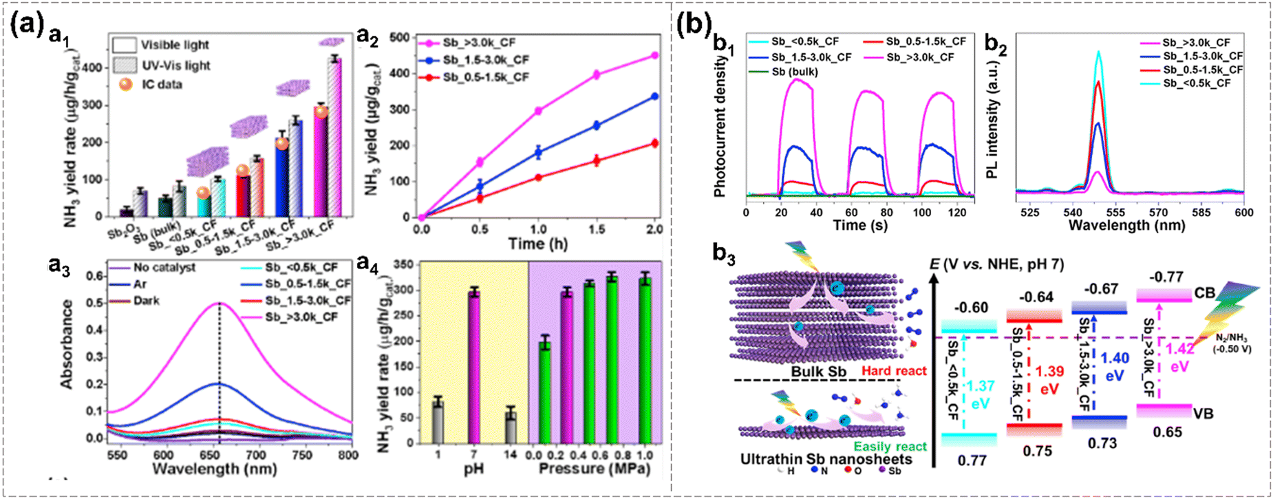 | ||
| Fig. 15 Photocatalytic N2 fixation and the energy band structures of Sb nanosheets.128 NH3 yield rates of Sb nanosheets over different cascade centrifugation (CF) speed tested by the indophenol blue method and ion chromatography (orange balls) (a1). NH3 yield of Sb nanosheets over reaction time (a2). Absorption spectra of Sb nanosheets in the dark, Ar atmosphere (under visible light), and without catalysts (under visible light) (a3). NH3 yield rate of Sb_ > 3.0k_CF under different pH values and pressure (a4). The photocurrent density of Sb nanosheets under different CF over time (b1). PL intensity of Sb nanosheets under different CF (b2). Schematic diagram of N2 fixation and the energy band structure of Sb nanosheets (b3). Reproduced from ref. 128 with permission from Elsevier, Copyright 2020. | ||
Furthermore, tellurene, antimonene and arsenene can be combined with other materials to enhance catalytic performance. They can act as the substrates for single atom catalysts (SACs) to interact with single-atom active sites or be used to form heterostructures with other layered 2D materials to achieve synergistic effects. For example, tellurene nanosheets are employed as metal-free cocatalysts and combined with CdS through a one-step hydrothermal method.126 The number of incident photons and quantum efficiency (QE) are calculated based on the following eqn (6) and (7), respectively.
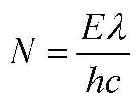 | (6) |
 | (7) |
This photocatalytic system exhibits a hydrogen production rate of 234.4 mmol h−1, a 7.8-fold improvement in catalytic activity compared to bare CdS (30.2 mmol h−1). A high wavelength-dependent apparent QE (AQE) of 11.4% and 5.6%, can be obtained at the fixed wavelength of 420 nm and 475 nm in prepared Te/CdS, respectively, which is comparable to most of the CdS merged with the previously reported metal-free and noble-metal-free cocatalysts.126 The formed favorable band alignment with photocatalysts and its thickness-dependent photocatalytic performance is investigated, revealing efficient electron–hole separation in the Te/CdS system.126 This is attributed to the fast electron transfer ability of tellurene suppresses the recombination of photo-generated charge on CdS.126
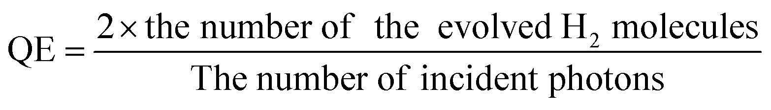
Additionally, atomic cobalt species (ACS) anchored to 2D tellurene are demonstrated as efficient photocatalysts for both the HER and CO2 reduction reactions (CO2RR). Tellurene acts as an active single-atom cocatalyst, anchoring ACS and bridging between the light absorber and ACS active sites for efficient electron transfer.27 The Co–Te bond forms between ACS and Te substrate, and its strong interaction leads to altered electronic structures in Te, creating intermediate energy states that can catch the photogenerated electron for better photocatalytic performance. As a result, the Te NS-ACS exhibit an outstanding enhanced visible-light photocatalytic H2 production rate of 130.8 μmol h−1 in the presence of Eosin Y (EY) as a light absorber, and a CO production rate of 52.3 μmol h−1 in the presence of tris(2,2′-bipyridyl) dichlororuthenium(II) ([Ru(bpy)3]Cl2) as a light absorber, representing the state-of-the-art noble-metal-free cocatalyst27 (Fig. 16).
 | ||
| Fig. 16 Photocatalytic performance and proposed mechanism of EY/Te NS-ACS (b) and [Ru(bpy)3]Cl2/Te NS-ACS (a), respectively.27 Time-dependent H2 evolution (a1) and H2 evolution rate (a2) of different materials. Cycling test of EY/Te NS-ACS for H2 evolution (a3). Proposed mechanism of EY/Te NS-ACS for H2 evolution (a4). CO and H2 evolution from CO2RR of different materials (b1). Cycling test of [Ru(bpy)3]Cl2/Te NS-ACS from CO2RR (b2). GC–MS (JEOL-GCQMS, JMS-K9, and 6890N Network GC) result of 13CO generated in the reduction of 13CO2 over [Ru(bpy)3]Cl2/Te NS-ACS (b3). Proposed mechanism for photocatalytic CO2RR over [Ru(bpy)3]Cl2/Te NS-ACS (b4). Reproduced from ref. 27 with permission from Wiley-VCH, Copyright 2020. | ||
Furthermore, 2D/2D graphitic carbon nitride/antimonene type I heterostructure (CNSbx) is prepared via a two-step procedure. It shows promoted light absorption, electron–hole separation capabilities, and higher photocatalytic activity for the degradation of organic pollutants, including rhodamine B (RhB) and p-nitrophenol (p-NP), compared with pristine carbon nitride (CN).129 The photochemical N-deethylation of RhB occurs through oxidation facilitated by photogenerated holes from the valence band of CN. However, electrons transferred from the conduction band of graphitic carbon nitride (g-CN) to the conduction band of Sb are also involved during the degradation process.129
The arsenene/g-C3N4 van der Waals heterostructure is theoretically studied for its potential application in water splitting.130 It exhibits improved optical absorption in both the visible light and ultraviolet regions compared to pristine monolayers. Thanks to their type-II band alignment and low exciton binding energy, they feature a solar-to-hydrogen (STH) efficiency limit of up to 15.8%, facilitating the effective separation of photogenerated electrons and holes.130 Besides, PtS2/arsenene van der Waals heterostructure is demonstrated to exhibit a direct Z-scheme catalytic.57 This PtS2/arsenene heterostructure is predicted to achieve an enhanced solar-to-hydrogen (STH) efficiency (49.32%) compared with isolated PtS2 (12.67%) or arsenene (10.34%) monolayers.57
5. Summary and perspectives
Antimonene, arsenene, tellurene and selenene possess remarkable inherent properties, including large specific areas, numerous active sites, outstanding conductivity, tunable bandgaps, and robust stability compared to phosphorene, making them highly promising materials for various catalytic applications. This review focuses on the recent advancements (publications from 2019 to 2023) concerning these four emerging Xenes. In addition to introducing the stable phases of these Xenes, along with their layer-dependent properties, particularly with regard to bandgap tunability, diverse preparation techniques, including top-down methods and bottom-up methods, are discussed. Engineering methods such as heterostructures, doping, defects and external strain fields, and applications in electrocatalysis, photocatalysis including HER, OER, ORR, CO2RR, NRR, and organic catalysis are introduced.It is noteworthy that these four Xenes are generally believed to exhibit limited inherent catalytic activity. Specifically, black and gray arsenene exhibit low catalytic performance due to their reduced molecular absorption capabilities. Additionally, these materials exhibit suboptimal photocatalytic ability owing to their unsuitable bandgaps, challenges in electron–hole separation, and rapid recombination rates. While the bulk form of these Xenes is reported to be stable, their monolayer or bilayer counterparts are prone to degradation in ambient environments. This instability complicates the acquisition of pure, defect-free forms of these four Xenes and poses challenges to the evaluation of their inherent physical and chemical properties. Moreover, reports on the large-scale synthesis of these Xenes are also limited, which hinders their industrial catalytic applications.
To address these challenges, scientists develop various engineering approaches to enhance the performance of these Xenes. For example, building heterostructures can minimize electron–hole recombination and align band edges with the requisite redox potentials for photocatalysis. Additionally, utilizing the large surface area, abundant active sites and high carrier mobility of antimonene to support transition metal SACs can improve gas molecular absorption and lower the overpotential. Moreover, machine learning and other advanced techniques are employed to identify optimal structures and properties for heterostructures and element doping combinations, streamlining the process and reducing manual labor. Furthermore, external safety measures such as protective coating are employed to minimize degradation during fabrication and storage.
Despite significant contributions, achieving large-scale synthesis of these Xenes with extended lateral dimensions remains a challenge. Additionally, a comprehensive understanding of the complex relationship between processing methods, structural changes, and resulting properties is crucial for bridging the gap between theoretical predictions and practical applications.
Author contributions
Cong Ma: conceptualization, methodology, formal analysis, investigation, writing – original draft; Kai Bao: formal analysis, validation, investigation, writing – review & editing; Junlei Qi: validation, writing– review & editing, supervision; Wenbin Wang: validation, investigation, resources; Jingkun Wu: validation, investigation; Ruijie Li: writing – review & editing, supervision; Yu Lin: writing – review & editing, supervision; Lingzhi Wang: validation; Zhuangzhuang Yin: validation; Zhixiang Tao: validation; Chengxuan Ke: supervision; Zongxiao Wu: supervision; Yingxia Liu: writing – review & editing, supervision, funding acquisition; Qiyuan He: writing – review & editing, supervision, funding acquisition.Data availability
No primary research results, software or code have been included and no new data were generated or analysed as part of this review.Conflicts of interest
The authors declare that they have no known competing financial interests or personal relationships that could have appeared to influence the work reported in this paper.Acknowledgements
Q. H. acknowledges the substantial support from the Research Grants Council of Hong Kong (projects no. 21302821 and 11314322). Yingxia Liu thanks the support from GRF-RGC General Research Fund (project no. CityU 11204824) and Shenzhen Science and Technology Innovation Commission (grant number SGDX20220530111203025).References
- Z. Q. Shi, H. Li, Q. Q. Yuan, Y. H. Song, Y. Y. Lv, W. Shi, Z. Y. Jia, L. Gao, Y. B. Chen and W. Zhu, van der Waals heteroepitaxial growth of monolayer Sb in a puckered honeycomb structure, Adv. Mater., 2019, 31, 1806130 CrossRef PubMed
.
- S. M. Beladi-Mousavi, A. M. Pourrahimi, Z. Sofer and M. Pumera, Atomically thin 2D-arsenene by liquid-phased exfoliation: toward selective vapor sensing, Adv. Funct. Mater., 2019, 29, 1807004 CrossRef
- A. Apte, S. Kouser, F. S. Samghabadi, L. Chang, L. M. Sassi, D. Litvinov, B. I. Yakobson, A. B. Puthirath and P. M. Ajayan, Piezo-response in two-dimensional α-Tellurene films, Mater. Today, 2021, 44, 40–47 CrossRef CAS
- R. Gusmão, Z. Sofer, D. Bouša and M. Pumera, Pnictogen (As, Sb, Bi) nanosheets for electrochemical applications are produced by shear exfoliation using kitchen blenders, Angew. Chem., Int. Ed., 2017, 129, 14609–14614 CrossRef
- W. Tian, S. Zhang, C. Huo, D. Zhu, Q. Li, L. Wang, X. Ren, L. Xie, S. Guo, P. K. Chu, H. Zeng and K. Huo, Few-layer antimonene: anisotropic expansion and reversible crystalline-phase evolution enable large-capacity and long-life Na-ion batteries, ACS Nano, 2018, 12, 1887–1893 CrossRef CAS PubMed
- T. Li, Y. Deng, X. Rong, C. He, M. Zhou, Y. Tang, H. Zhou, C. Cheng and C. Zhao, Nanostructures and catalytic atoms engineering of tellurium-based materials and their roles in electrochemical energy conversion, SmartMat, 2023, 4, e1142 CrossRef CAS
- S. Noreen, M. B. Tahir, A. Hussain, T. Nawaz, J. U. Rehman, A. Dahshan, M. Alzaid and H. Alrobei, Emerging 2D-nanostructured materials for electrochemical and sensing application-a review, Int. J. Hydrogen Energy, 2022, 47, 1371–1389 CrossRef CAS
- Y. Chen, C. Chen, R. Kealhofer, H. Liu, Z. Yuan, L. Jiang, J. Suh, J. Park, C. Ko, H. S. Choe, J. Avila, M. Zhong, Z. Wei, J. Li, S. Li, H. Gao, Y. Liu, J. Analytis, Q. Xia, M. C. Asensio and J. Wu, Black arsenic: a Layered semiconductor with extreme in-plane anisotropy, Adv. Mater., 2018, 30, 1800754 CrossRef PubMed
- Q. Junlei, D. Yongping, M. Chen, K. Chengxuan, W. Wenbin, W. Zongxiao, W. Xiang, B. Kai, X. Yue and H. Haoxin, Surfactant-free ultrasonication-assisted synthesis of 2D tellurium based on metastable 1T′-MoTe2, Adv. Mater., 2023, 36, 2306962 Search PubMed
- H. Huang, J. Zha, S. Xu, P. Yang, Y. Xia, H. Wang, D. Dong, L. Zheng, Y. Yao and Y. Zhang, Precursor-confined chemical vapor deposition of 2D single-crystalline SexTe1–x nanosheets for p-type transistors and inverters, ACS Nano, 2024, 18, 17293–17303 CrossRef CAS PubMed
- H. Jiang, L. Zheng, Z. Liu and X. Wang, Two-dimensional materials: from mechanical properties to flexible mechanical sensors, InfoMat, 2020, 2, 1077–1094 CrossRef CAS
- S. Guo, Y. Zhang, Y. Ge, S. Zhang, H. Zeng and H. Zhang, 2D V-V binary materials: status and challenges, Adv. Mater., 2019, 31, 1902352 CrossRef PubMed
- J. A. Carrasco, P. Congost-Escoin, M. Assebban and G. Abellán, Antimonene: a tuneable post-graphene material for advanced applications in optoelectronics, catalysis, energy and biomedicine, Chem. Soc. Rev., 2023, 52, 1288–1330 RSC
- Z. Wu, J. Qi, W. Wang, Z. Zeng, Q. He and Z. Wu, Emerging elemental two-dimensional materials for energy applications, J. Mater. Chem. A, 2021, 9, 18793–18817 RSC
- R. Hu, G. Liao, Z. Huang, H. Qiao, H. Liu, Y. Shu, B. Wang and X. Qi, Recent advances of monoelemental 2D materials for photocatalytic applications, J. Hazard. Mater., 2021, 405, 124179 CrossRef CAS PubMed
- Z. Xie, B. Zhang, Y. Ge, Y. Zhu, G. Nie, Y. Song, C.-K. Lim, H. Zhang and P. N. Prasad, Chemistry, functionalization, and applications of recent monoelemental two-dimensional materials and their heterostructures, Chem. Rev., 2021, 122, 1127–1207 CrossRef PubMed
- N. R. Glavin, R. Rao, V. Varshney, E. Bianco, A. Apte, A. Roy, E. Ringe and P. M. Ajayan, Emerging applications of elemental 2D materials, Adv. Mater., 2020, 32, 1904302 CrossRef CAS PubMed
- L. Zhang, T. Gong, Z. Yu, H. Dai, Z. Yang, G. Chen, J. Li, R. Pan, H. Wang, Z. Guo, H. Zhang and X. Fu, Recent advances in hybridization, doping, and functionalization of 2D Xenes, Adv. Funct. Mater., 2021, 31, 2005471 CrossRef CAS
- H.-F. Wang, C. Tang, C.-X. Zhao, J.-Q. Huang and Q. Zhang, Emerging graphene derivatives and analogues for efficient energy electrocatalysis, Adv. Funct. Mater., 2022, 32, 2204755 CrossRef CAS
- C. C. Mayorga-Martinez, R. Gusmão, Z. Sofer and M. Pumera, Pnictogen-based enzymatic phenol biosensors: phosphorene, arsenene, antimonene, and bismuthene, Angew. Chem., Int. Ed., 2019, 58, 134–138 CrossRef CAS PubMed
- Y. Hu, J. Liang, Y. Xia, C. Zhao, M. Jiang, J. Ma, Z. Tie and Z. Jin, 2D arsenene and arsenic materials: fundamental properties, preparation, and applications, Small, 2022, 18, 2104556 CrossRef CAS PubMed
- W. Zhang, X. Zhang, L. K. Ono, Y. Qi and H. Oughaddou, Recent advances in phosphorene: structure, synthesis, and properties, Small, 2023, 2303115 Search PubMed
- X. Ye, M. Qi, M. Chen, L. Zhang and J. Zhang, Zero to three dimension structure evolution from carbon allotropes to phosphorus allotropes, Adv. Mater. Interfaces, 2023, 10, 2201941 CrossRef CAS
- S. Yadav, M. A. Sadique, A. Kaushik, P. Ranjan, R. Khan and A. K. Srivastava, Borophene as an emerging 2D flatland for biomedical applications: current challenges and future prospects, J. Mater. Chem. B, 2022, 10, 1146–1175 RSC
- C. Hou, G. Tai, Y. Liu, Z. Wu, X. Liang and X. Liu, Borophene-based materials for energy, sensors and information storage applications, Nano Res. Energy, 2023, 2, e9120051 CrossRef
- W. Zheng, Y. Li, M. Liu and L. Y. S. Lee, Few-layer tellurium: cathodic exfoliation and doping for collaborative hydrogen evolution, Small, 2021, 17, 2007768 CrossRef CAS PubMed
- L. Shi, X. Ren, Q. Wang, Y. Li, F. Ichihara, H. Zhang, Y. Izumi, L. Ren, W. Zhou and Y. Yang, Stabilizing atomically dispersed catalytic sites on tellurium nanosheets with strong metal-support interaction boosts photocatalysis, Small, 2020, 16, 2002356 CrossRef CAS PubMed
- X. Cai, X. Jia, Y. Liu, L. Zhang, W. Yu, B. Wang, X. Yang, Q. Wang and Y. Jia, Enhanced carrier mobility and tunable electronic properties in α-tellurene monolayer via an α-tellurene and h-BN heterostructure, Phys. Chem. Chem. Phys., 2020, 22, 6434–6440 RSC
- T. Niu, Q. Meng, D. Zhou, N. Si, S. Zhai, X. Hao, M. Zhou and H. Fuchs, Large-scale synthesis of strain-tunable semiconducting antimonene on copper oxide, Adv. Mater., 2020, 32, 1906873 CrossRef CAS PubMed
- T. Wang, H. Wang, Z. Kou, W. Liang, X. Luo, F. Verpoort, Y.-J. Zeng and H. Zhang, Xenes as an emerging 2D monoelemental family: fundamental electrochemistry and energy applications, Adv. Funct. Mater., 2020, 30, 2002885 CrossRef CAS
- P. Hess, Bonding, structure, and mechanical stability of 2D materials: the predictive power of the periodic table, Nanoscale Horiz., 2021, 6, 856–892 RSC
- Y. Hu, Z.-H. Qi, J. Lu, R. Chen, M. Zou, T. Chen, W. Zhang, Y. Wang, X. Xue and J. Ma, van der Waals epitaxial growth and interfacial passivation of two-dimensional single-crystalline few-layer gray arsenic nanoflakes, Chem. Mater., 2019, 31, 4524–4535 CrossRef CAS
- T. Niu, W. Zhou, D. Zhou, X. Hu, S. Zhang, K. Zhang, M. Zhou, H. Fuchs and H. Zeng, Modulating epitaxial atomic structure of antimonene through interface design, Adv. Mater., 2019, 31, 1902606 CrossRef PubMed
- L. Peng, S. Ye, J. Song and J. Qu, Solution-phase synthesis of few-layer hexagonal antimonene nanosheets via anisotropic growth, Angew. Chem., Int. Ed., 2019, 58, 9891–9896 CrossRef CAS PubMed
- P. Ares, F. Aguilar-Galindo, D. Rodríguez-San-Miguel, D. A. Aldave, S. Díaz-Tendero, M. Alcamí, F. Martín, J. Gómez-Herrero and F. Zamora, Mechanical isolation of highly stable antimonene under ambient conditions, Adv. Mater., 2016, 28, 6332–6336 CrossRef CAS PubMed
- K. Luo, S. Chen and C. Duan, Indirect-direct band gap transition of two-dimensional arsenic layered semiconductors-cousins of black phosphorus, Sci. China: Phys., Mech. Astron., 2015, 58, 87301 Search PubMed
- S. Santisouk, P. Sengdala, X. Jiang, X.-X. Xue, K.-Q. Chen and Y. Feng, Tuning the electrocatalytic properties of black and gray arsenene by introducing heteroatoms, ACS Omega, 2021, 6, 13124–13133 CrossRef CAS PubMed
- H. Yun, S. Ghosh, P. Golani, S. J. Koester and K. A. Mkhoyan, Layer dependence of dielectric response and water-enhanced ambient degradation of highly anisotropic black As, ACS Nano, 2020, 14, 5988–5997 CrossRef CAS PubMed
- Z. Wu, J. Qi, W. Wang, P. Yang, C. Ma, H. Huang, K. Bao, J. Wu, C. Ke, Y. Chen, C. Tan, D. V. M. Repaka and Q. He, Iontronic and electrochemical investigations of 2D tellurene in aqueous electrolytes, SmartMat, 2023, 5, e1234 CrossRef
- Y. Hu, X. Wang, Z. Qi, S. Wan, J. Liang, Q. Jia, D. Hong, Y. Tian, J. Ma and Z. Tie, Wet chemistry vitrification and metal-to-semiconductor transition of 2D gray arsenene nanoflakes, Adv. Funct. Mater., 2021, 31, 2106529 CrossRef CAS
- J. Shah, W. Wang, H. M. Sohail and R. Uhrberg, Experimental evidence of monolayer arsenene: an exotic 2D semiconducting material, 2D Mater., 2020, 7, 025013 CrossRef CAS
- E. Kovalska, N. Antonatos, J. Luxa and Z. Sofer, “Top-down” arsenene production by low-potential electrochemical exfoliation, Inorg. Chem., 2020, 59, 11259–11265 CrossRef CAS PubMed
- J. Barrio, C. Gibaja, M. García-Tecedor, L. Abisdris, I. Torres, N. Karjule, S. Giménez, M. Shalom and F. Zamora, Electrophoretic deposition of antimonene for photoelectrochemical applications, Appl. Mater. Today, 2020, 20, 100714 CrossRef
- Y. Han, T. Zuo, K. He, L. Yang, S. Zhan, Z. Liu, Z. Ma, J. Xu, Y. Che and W. Zhao, 2D-Antimonene-assisted hetero-epitaxial growth of perovskite films for efficient solar cells, Mater. Today, 2022, 61, 54–64 CrossRef CAS
- M. Bat-Erdene, G. Xu, M. Batmunkh, A. S. R. Bati, J. J. White, M. J. Nine, D. Losic, Y. Chen, Y. Wang, T. Ma, J. G. Shapter and M. Bat-Erdene, Surface oxidized two-dimensional antimonene nanosheets for electrochemical ammonia synthesis under ambient conditions, J. Mater. Chem. A, 2020, 8, 4735–4739 RSC
- J. Zhang, S. Ye, Y. Sun, F. Zhou, J. Song and J. Qu, Soft-template assisted synthesis of hexagonal antimonene and bismuthene in colloidal solutions, Nanoscale, 2020, 12, 20945–20951 RSC
- Z. Shi, H. Li, C. Xue, Q. Yuan, Y. Lv, Y. Xu, Z. Jia, L. Gao, Y. Chen and W. Zhu, Tuning the electronic structure of an α-antimonene monolayer through interface engineering, Nano Lett., 2020, 20, 8408–8414 CrossRef CAS PubMed
- P. V. Sarma, R. Nadarajan, R. Kumar, R. M. Patinharayil, N. Biju, S. Narayanan, G. Gao, C. S. Tiwary, M. Thalakulam, R. N. Kini, A. K. Singh, P. M. Ajayan and M. M. Shaijumon, Growth of highly crystalline ultrathin two-dimensional selenene, 2D Mater., 2022, 9, 045004 CrossRef CAS
- J. Y. Park, M. S. Moon, H. Lee, D. Kim, H. Park, J. W. Kim, H. Ko, T. Ha, J. Kim, Y.-M. Bahk, B. H. Moon, K. K. Kim, S. R. Park, S. Choi, R. Sebait, J. H. Kim, Y. H. Lee and G. H. Han, Continuous template growth of large-scale tellurene films on 1T′-MoTe2, ACS Nano, 2024, 18, 18992–19002 CrossRef CAS PubMed
- S. Kang, T. Dai, X. Ma, S. Dang, H. Li, P. Hu, F. Yu, X. Zhou, S. Wu and S. Li, Broad spectral response of an individual tellurium nanobelt grown by molecular beam epitaxy, Nanoscale, 2019, 11, 1879–1886 RSC
- C. Zhao, C. Tan, D.-H. Lien, X. Song, M. Amani, M. Hettick, H. Y. Y. Nyein, Z. Yuan, L. Li and M. C. Scott, Evaporated tellurium thin films for p-type field-effect transistors and circuits, Nat. Nanotechnol., 2020, 15, 53–58 CrossRef CAS PubMed
- C. Shen, Y. Liu, J. Wu, C. Xu, D. Cui, Z. Li, Q. Liu, Y. Li, Y. Wang, X. Cao, H. Kumazoe, F. Shimojo, A. Krishnamoorthy, R. K. Kalia, A. Nakano, P. D. Vashishta, M. R. Amer, A. N. Abbas, H. Wang, W. Wu and C. Zhou, Tellurene photodetector with high gain and wide bandwidth, ACS Nano, 2019, 14, 303–310 CrossRef PubMed
- G. Qiu, C. Niu, Y. Wang, M. Si, Z. Zhang, W. Wu and P. D. Ye, Quantum Hall effect of Weyl fermions in n-type semiconducting tellurene, Nat. Nanotechnol., 2020, 15, 585–591 CrossRef CAS PubMed
- J. Zhou, G. Zhang, W. Wang, Q. Chen, W. Zhao, H. Liu, B. Zhao, Z. Ni and J. Lu, Phase-engineered synthesis of atomically thin te single crystals with high on-state currents, Nat. Commun., 2024, 15, 1435 CrossRef CAS PubMed
- R. Bhuvaneswari, V. Nagarajan and R. Chandiramouli, Recent advances in arsenene nanostructures towards prediction, properties, synthesis and applications, Surf. Interfaces, 2022, 28, 101610 CrossRef CAS
- B. Zhang, H. Zhang, J. Lin, X. Cheng and B. Zhang, First-principle study of seven allotropes of arsenene and antimonene: thermodynamic, electronic and optical properties, Phys. Chem. Chem. Phys., 2018, 20, 30257–30266 RSC
- K. Ren, W. Tang, M. Sun, Y. Cai, Y. Cheng and G. Zhang, A direct Z-scheme PtS2/arsenene van der Waals heterostructure with high photocatalytic water splitting efficiency, Nanoscale, 2020, 12, 17281–17289 RSC
- Q. Lu, L. Zhang, T. Xu, B. Zhang and W. Gong, Highly efficient photocatalytic water splitting in direct Z-scheme α-In2Se3/Are van der Waals heterostructures, Surf. Interfaces, 2023, 36, 102608 CrossRef CAS
- Z. Xu, R. Song, M. Wang, X. Zhang, G. Liu and G. Qiao, Single atom-doped arsenene as electrocatalyst for reducing nitrogen to ammonia: a DFT study, Phys. Chem. Chem. Phys., 2020, 22, 26223–26230 RSC
- A. Chen, J. Cai, Z. Wang, Y. Han, S. Ye and J. Li, An ensemble learning classifier to discover arsenene catalysts with implanted heteroatoms for hydrogen evolution reaction, J. Energy Chem., 2023, 78, 268–276 CrossRef CAS
- M. Zhong, Q. Xia, L. Pan, Y. Liu, Y. Chen, H.-X. Deng, J. Li and Z. Wei, Thickness-dependent carrier transport characteristics of a new 2D elemental semiconductor: black arsenic, Adv. Funct. Mater., 2018, 28, 1802581 CrossRef
- P. Wu and M. Huang, Transition metal doped arsenene: promising materials for gas sensing, catalysis and spintronics, Appl. Surf. Sci., 2020, 506, 144660 CrossRef CAS
- S. Shen, Y. Gan, X.-X. Xue, J. Wei, L.-M. Tang, K. Chen and Y. Feng, Role of defects on the catalytic property of 2D black arsenic for hydrogen evolution reaction, Appl. Phys. Express, 2019, 12, 075502 CrossRef
- Q. Zhou, W. Ju, Y. Liu, J. Li and Q. Zhang, Influence of defects and dopants on the sensitivity of arsenene towards HCN, Appl. Surf. Sci., 2020, 506, 144936 CrossRef CAS
- Y. Liu, Q. Zhou, W. Ju, J. Li and Y. Liu, Influence of the vacancy-defect and transition-metal doping in arsenene: a first-principles study, Superlattices Microstruct., 2019, 132, 106163 CrossRef CAS
- X. T. Zhu, Y. Xu, Y. Cao and W. Sheng, Direct Z-scheme arsenene/HfS2 van der Waals heterojunction for overall photocatalytic water splitting: first-principles study, Appl. Surf. Sci., 2022, 574, 151650 CrossRef CAS
- J. Li, Z. Huang, W. Ke, J. Yu, K. Ren and Z. Dong, High solar-to-hydrogen efficiency in Arsenene/GaX (X = S, Se) van der Waals heterostructure for photocatalytic water splitting, J. Alloys Compd., 2021, 866, 158774 CrossRef CAS
- P. Wu and M. Huang, Investigation of adsorption behaviors, and electronic and magnetic properties for small gas molecules adsorbed on Pt-doped arsenene by density functional calculations, RSC Adv., 2023, 13, 3807–3817 RSC
- S. S. Chauhan, S. Ferwani and P. Srivastava, Effect of strain on the structural and electronic properties of transition metal-doped arsenene nanoribbons: an ab-initio approach, Pramana, 2019, 93, 45 CrossRef
- M. Assebban, C. Gibaja, M. Fickert, I. Torres, E. Weinreich, S. Wolff, R. Gillen, J. Maultzsch, M. Varela, S. Tan Jun Rong, K. P. Loh, E. G. Michel, F. Zamora and G. Abellán, Unveiling the oxidation behavior of liquid-phase exfoliated antimony nanosheets, 2D Mater., 2020, 7, 025039 CrossRef CAS
- Y. Li, J. Chen, J. Huang, Y. Hou, L. Lei, W. Lin, Y. Lian, X. Zhonghua, H. Yang and Z. Wen, Interfacial engineering of Ru–S–Sb/antimonene electrocatalysts for highly efficient electrolytic hydrogen generation in neutral electrolyte, Chem. Commun., 2019, 55, 10884–10887 RSC
- S. Cao, Y. Sun, S. Guo, Z. Guo, Y. Feng, S. Chen, H. Chen, S. Zhang and F. Jiang, Defect regulating of few-layer antimonene from acid-assisted exfoliation for enhanced electrocatalytic nitrogen fixation, ACS Appl. Mater. Interfaces, 2021, 13, 40618–40628 CrossRef CAS PubMed
- A. Bafekry, M. Ghergherehchi and S. F. Shayesteh, Tuning the electronic and magnetic properties of antimonene nanosheets via point defects and external fields: first-principles calculations, Phys. Chem. Chem. Phys., 2019, 21, 10552–10566 RSC
- D. Singh and R. Ahuja, Theoretical prediction of a Bi-doped β-Antimonene monolayer as a highly efficient photocatalyst for oxygen reduction and overall water splitting, ACS Appl. Mater. Interfaces, 2021, 13, 56254–56264 CrossRef CAS PubMed
- S. Dai, Y.-L. Lu and P. Wu, Tuning electronic, magnetic and optical properties of Cr-doped antimonene via biaxial strain engineering, Appl. Surf. Sci., 2019, 463, 492–497 CrossRef CAS
- X. Fan, Y. Li, L. Su, K. Ma, J. Li and H. Zhang, Theoretical prediction of tunable electronic and magnetic properties of monolayer antimonene by vacancy and strain, Appl. Surf. Sci., 2019, 488, 98–106 CrossRef CAS
- Y. Wu, K. Xu, C. Ma, Y. Chen, Z. Lu, H. Zhang, Z. Fang and R. Zhang, Ultrahigh carrier mobilities and high thermoelectric performance at room temperature optimized by strain-engineering to two-dimensional aw-antimonene, Nano Energy, 2019, 63, 103870 CrossRef CAS
- Q. Zhang, Y. Tseng, K. Lu, C. Huang, H. Hsu and W. Wu, Epitaxial growth and e-beam induced structural changes of single crystalline 2D antimonene, Scr. Mater., 2023, 226, 115262 CrossRef CAS
- S. Sun, T. Yang, Y. Z. Luo, J. Gou, Y. Huang, C. Gu, Z. Ma, X. Lian, S. Duan and A. T. Wee, Realization of a buckled antimonene monolayer on Ag (111) via surface engineering, J. Phys. Chem. Lett., 2020, 11, 8976–8982 CrossRef CAS PubMed
- J. Singh, P. Jamdagni, M. Jakhar and A. Kumar, Stability, electronic and mechanical properties of chalcogen (Se and Te) monolayers, Phys. Chem. Chem. Phys., 2020, 22, 5749–5755 RSC
- C. Liu, T. Hu, Y. Wu, H. Gao, Y. Yang and W. Ren, 2D selenium allotropes from first principles and swarm intelligence, J. Phys.: Condens. Matter, 2019, 31, 235702 CrossRef CAS PubMed
- Y. Suzuki, F. Doi, N. Urakami and Y. Hashimoto, Crystalline trigonal selenium flakes grown by vapor deposition and its photodetector application, Mater. Lett., 2020, 275, 128207 CrossRef CAS
- S. Prodhan, K. K. Chauhan, T. Singha, M. Karmakar, N. Maity, R. Nadarajan, P. Kumbhakar, C. S. Tiwary, A. K. Singh and M. M. Shaijumon, Comprehensive excited state carrier dynamics of 2D selenium: one-photon and multi-photon absorption regimes, Appl. Phys. Lett., 2023, 123, 021105 CrossRef CAS
- J. Min, C. Zhao, Z. Zeng, Y. Jia and Z. Du, Tunable visible-light excitonic absorption and high photoconversion efficiency in two-dimensional group-VI monolayer materials, Phys. Rev. B, 2019, 100, 085402 CrossRef CAS
- L. Ramírez-Montes, M. G. Moreno-Armenta, J. Guerrero-Sánchez, R. Ponce-Pérez, R. González-Hernández and W. López-Pérez, Tuning the electronic and thermoelectric properties of selenium monolayers through atomic impurities: A DFT study, Solid State Commun., 2023, 371, 115268 CrossRef
- S. Demirci, H. H. Gürel, S. Jahangirov and S. Ciraci, Temperature, strain and charge mediated multiple and dynamical phase changes of selenium and tellurium, Nanoscale, 2020, 12, 3249–3258 RSC
- F. Calavalle, M. Suárez-Rodríguez, B. Martín-García, A. Johansson, D. C. Vaz, H. Yang, I. V. Maznichenko, S. Ostanin, A. Mateo-Alonso, A. Chuvilin, I. Mertig, M. Gobbi, F. Casanova and L. E. Hueso, Gate-tuneable and chirality-dependent charge-to-spin conversion in tellurium nanowires, Nat. Mater., 2022, 21, 526–532 CrossRef CAS PubMed
- X. Huang, R. Xiong, C. Hao, W. Li, B. Sa, J. Wiebe and R. Wiesendanger, Experimental realization of monolayer α-tellurene, Adv. Mater., 2024, 36, 2309023 CrossRef CAS PubMed
- C. Zhao, H. Batiz, B. Yasar, H. Kim, W. Ji, M. C. Scott, D. C. Chrzan and A. Javey, Tellurium single-crystal arrays by low-temperature evaporation and crystallization, Adv. Mater., 2021, 33, 2100860 CrossRef CAS PubMed
- X. Zhang, J. Jiang, A. A. Suleiman, B. Jin, X. Hu, X. Zhou and T. Zhai, Hydrogen-assisted growth of ultrathin Te flakes with giant gate-dependent photoresponse, Adv. Funct. Mater., 2019, 29, 1906585 CrossRef CAS
- G. Jnawali, Y. Xiang, S. M. Linser, I. A. Shojaei, R. Wang, G. Qiu, C. Lian, B. M. Wong, W. Wu and P. D. Ye, Ultrafast photoinduced band splitting and carrier dynamics in chiral tellurium nanosheets, Nat. Commun., 2020, 11, 3991 CrossRef CAS PubMed
- S. Zhao, B. Dong, H. Wang, H. Wang, Y. Zhang, Z. V. Han, H. Zhang and S. Zhao, In-plane anisotropic electronics based on low-symmetry 2D materials: progress and prospects, Nanoscale Adv., 2020, 2, 109–139 RSC
- D. Wines, J. A. Kropp, G. Chaney, F. Ersan and C. Ataca, Electronic properties of bare and functionalized two-dimensional (2D) tellurene structures, Phys. Chem. Chem. Phys., 2020, 22, 6727–6737 RSC
- H. Ma, W. Hu and J. Yang, Control of highly anisotropic electrical conductance of tellurene by strain-engineering, Nanoscale, 2019, 11, 21775–21781 RSC
- P. K. Sachdeva, S. Gupta and C. Bera, Large piezoelectric and thermal expansion coefficients with negative Poisson's ratio in strain-modulated tellurene, Nanoscale Adv., 2021, 3, 3279–3287 RSC
- X. Cai, Y. Ren, M. Wu, D. Xu and X. Luo, Strain-induced phase transition and giant piezoelectricity in monolayer tellurene, Nanoscale, 2020, 12, 167–172 RSC
- Y. Dong, B. Zeng, X. Zhang, D. Li, J. He and M. Long, Study on the strain-induced mechanical property modulations in monolayer tellurene, J. Appl. Phys., 2019, 125, 064304 CrossRef
- R. Han, M. Qi, Z. Mao, X. Lin and P. Wu, Strain-improved electronic and magnetic properties of V-, Cr-, Mn-and Fe-doped α-and β-tellurene, Appl. Surf. Sci., 2021, 541, 148454 CrossRef CAS
- H. K. Mishra, Ankush, N. Barman, B. Mondal, M. Jha, R. Thapa and D. Mandal, Beyond conventional catalysts: monoelemental tellurium as a game changer for piezo-driven hydrogen evolution, Small, 2024, 20, 2402421 CrossRef CAS PubMed
- W. Xu, L. Gan, R. Wang, X. Wu and H. Xu, Surface adsorption and vacancy in tuning the properties of tellurene, ACS Appl. Mater. Interfaces, 2020, 12, 19110–19115 CrossRef CAS PubMed
- J. Qiao, Y. Pan, F. Yang, C. Wang, Y. Chai and W. Ji, Few-layer tellurium: one-dimensional-like layered elementary semiconductor with striking physical properties, Sci. Bull., 2018, 63, 159–168 CrossRef CAS PubMed
- Z. Shi, R. Cao, K. Khan, A. K. Tareen, X. Liu, W. Liang, Y. Zhang, C. Ma, Z. Guo, X. Luo and H. Zhang, Two-dimensional tellurium: progress, challenges, and prospects, Nano-Micro Lett., 2020, 12, 99 CrossRef CAS PubMed
- K. Wu, H. Ma, Y. Gao, W. Hu and J. Yang, Highly-efficient heterojunction solar cells based on two-dimensional tellurene and transition metal dichalcogenides, J. Mater. Chem. A, 2019, 7, 7430–7436 RSC
- Y. Xiang, S. Gao, R.-G. Xu, W. Wu and Y. Leng, Phase transition in two-dimensional tellurene under mechanical strain modulation, Nano Energy, 2019, 58, 202–210 CrossRef CAS
- G. Qiu, S. Huang, M. Segovia, P. K. Venuthurumilli, Y. Wang, W. Wu, X. Xu and P. D. Ye, Thermoelectric performance of 2D tellurium with accumulation contacts, Nano Lett., 2019, 19, 1955–1962 CrossRef CAS PubMed
- I. Torres, M. Alcaraz, R. Sanchis-Gual, J. A. Carrasco, M. Fickert, M. Assebban, C. Gibaja, C. Dolle, D. A. Aldave, C. Gómez-Navarro, S. Elena, E. G. Michel, M. Varela, J. Gómez-Herrero, G. Abellán and F. Zamora, Continuous-flow synthesis of high-quality few-layer antimonene hexagons, Adv. Funct. Mater., 2021, 31, 2101616 CrossRef CAS
- X. Wu, Y. Shao, H. Liu, Z. Feng, Y.-L. Wang, J.-T. Sun, C. Liu, J.-O. Wang, Z.-L. Liu, S.-Y. Zhu, Y.-Q. Wang, S.-X. Du, Y.-G. Shi, K. Ibrahim and H.-J. Gao, Epitaxial growth and air-stability of monolayer antimonene on PdTe2, Adv. Mater., 2017, 29, 1605407 CrossRef PubMed
- H. O. H. Churchill, G. J. Salamo, S.-Q. Yu, T. Hironaka, X. Hu, J. Stacy and I. Shih, Toward single atom chains with exfoliated tellurium, Nanoscale Res. Lett., 2017, 12, 488 CrossRef PubMed
- J. Qi, Z. Wu, W. Wang, K. Bao, L. Wang, J. Wu, C. Ke, Y. Xu and Q. He, Fabrication and applications of van der Waals heterostructures, Int. J. Extreme Manuf., 2023, 5, 022007 CrossRef CAS
- Q. Yu, C. Chen, K. Guo, H. Deng, T. Yi, Y. Zhang, W. Su, J. Wu and K. Zhang, Deterministic transfer of large-scale β-phase arsenic on fiber end cap for near-infrared ultrafast pulse generation, Front. Mater., 2021, 8, 721587 CrossRef
- P. Ares, F. Zamora and J. Gomez-Herrero, Optical identification of few-layer antimonene crystals, ACS Photonics, 2017, 4, 600–605 CrossRef CAS
- C. Gibaja, M. Assebban, I. Torres, M. Fickert, R. Sanchis-Gual, I. Brotons, W. S. Paz, J. J. Palacios, E. G. Michel, G. Abellán, F. Zamora and C. Gibaja, Liquid phase exfoliation of antimonene: systematic optimization, characterization and electrocatalytic properties, J. Mater. Chem. A, 2019, 7, 22475–22486 RSC
- W. Zheng and L. Y. S. Lee, Beyond sonication: advanced exfoliation methods for scalable production of 2D materials, Matter, 2022, 5, 515–545 CrossRef CAS
- Y. Zhang, M. Qiao, Y. Huang, Y. Zou, Z. Liu, L. Tao, Y. Li, C.-L. Dong and S. Wang, In situ exfoliation and Pt deposition of antimonene for formic acid oxidation via a predominant dehydrogenation pathway, Research, 2020, 2020, 5487237 CAS
- M. V. Bracamonte, G. I. Lacconi, S. E. Urreta and L. E. F. Foa Torres, On the nature of defects in liquid-phase exfoliated graphene, J. Phys. Chem. C, 2014, 118, 15455–15459 CrossRef CAS
- W. Wu, G. Qiu, Y. Wang, R. Wang, P. Ye and W. Wu, Tellurene: its physical properties, scalable nanomanufacturing, and device applications, Chem. Soc. Rev., 2018, 47, 7203–7212 RSC
- M. Peng, R. Xie, Z. Wang, P. Wang, F. Wang, H. Ge, Y. Wang, F. Zhong, P. Wu and J. Ye, Blackbody-sensitive room-temperature infrared photodetectors based on low-dimensional tellurium grown by chemical vapor deposition, Sci. Adv., 2021, 7, eabf7358 CrossRef CAS PubMed
- S. Dongre S, R. Shwetharani, C. Hunsur Ravikumar, C. Lavanya and R. G. Balakrishna, Review on 2D arsenene and antimonene: emerging materials for energy, electronic and biological applications, Adv. Mater. Interfaces, 2022, 9, 2200442 CrossRef CAS
- J. Rathore and S. Mahapatra, Formation of antimonene nanoribbons by molecular beam epitaxy, 2D Mater., 2020, 7, 045003 CrossRef CAS
- Y. Wang, G. Qiu, R. Wang, S. Huang, Q. Wang, Y. Liu, Y. Du, W. A. Goddard, M. J. Kim, X. Xu, P. D. Ye and W. Wu, Field-effect transistors made from solution-grown two-dimensional tellurene, Nat. Electron., 2018, 1, 228–236 CrossRef
- C. Li, L. Zhang, T. Gong, Y. Cheng, L. Li, L. Li, S. Jia, Y. Qi, J. Wang and Y. Gao, Study of the growth mechanism of solution-synthesized symmetric tellurium nanoflakes at atomic resolution, Small, 2021, 17, 2005801 CrossRef CAS PubMed
- X. Ren, Z. Li, H. Qiao, W. Liang, H. Liu, F. Zhang, X. Qi, Y. Liu, Z. Huang, D. Zhang, J. Li, J. Zhong and H. Zhang, Few-layer antimonene nanosheet: a metal-free bifunctional electrocatalyst for effective water splitting, ACS Appl. Energy Mater., 2019, 2, 4774–4781 CrossRef CAS
- V. Lloret, M. Á. Rivero-Crespo, J. A. Vidal-Moya, S. Wild, A. Doménech-Carbó, B. S. Heller, S. Shin, H.-P. Steinrück, F. Maier and F. Hauke, Few layer 2D pnictogens catalyze the alkylation of soft nucleophiles with esters, Nat. Commun., 2019, 10, 509 CrossRef PubMed
- J. Liu, J. J. Hinsch, H. Yin, P. Liu, H. Zhao and Y. Wang, β-arsenene monolayer: a promising electrocatalyst for anodic chlorine evolution reaction, Catalysts, 2022, 12, 296 CrossRef CAS
- S. Lu, H. L. Huynh, F. Lou, K. Guo and Z. Yu, Single transition metal atom embedded antimonene monolayers as efficient trifunctional electrocatalysts for the HER, OER and ORR: a density functional theory study, Nanoscale, 2021, 13, 12885–12895 RSC
- B. Qiu, C. Wang, J. Wang, Z. Lin, N. Zhang, L. Cai, X. Tao and Y. Chai, Metal-free tellurene cocatalyst with tunable bandgap for enhanced photocatalytic hydrogen production, Mater. Today Energy, 2021, 21, 100720 CrossRef CAS
- A. Kokabi and S. B. Touski, Electronic and photocatalytic properties of antimonene nanosheets, Phys. E, 2020, 124, 114336 CrossRef CAS
- Z. Zhao, C. Choi, S. Hong, H. Shen, C. Yan, J. Masa, Y. Jung, J. Qiu and Z. Sun, Surface-engineered oxidized two-dimensional Sb for efficient visible light-driven N2 fixation, Nano Energy, 2020, 78, 105368 CrossRef CAS
- J. Barrio, C. Gibaja, J. Tzadikov, M. Shalom and F. Zamora, 2D/2D graphitic carbon nitride/antimonene heterostructure: structural characterization and application in photocatalysis, Adv. Sustain. Syst., 2019, 3, 1800138 CrossRef
- X.-H. Li, B.-J. Wang, G.-D. Wang, X.-F. Yang, R.-Q. Zhao, X.-T. Jia and S.-H. Ke, A two-dimensional arsenene/g-C3N4 van der Waals heterostructure: a highly efficient photocatalyst for water splitting, Sustainable Energy Fuels, 2021, 5, 2249–2256 RSC
Footnote |
| † Cong Ma and Kai Bao contributed equally to this work. |
| This journal is © the Partner Organisations 2025 |