DOI:
10.1039/D4RA05770H
(Paper)
RSC Adv., 2025,
15, 1020-1032
Electronic and magnetic properties of GeP monolayer modulated by Ge vacancies and doping with Mn and Fe transition metals
Received
9th August 2024
, Accepted 20th December 2024
First published on 13th January 2025
Abstract
In this work, Ge vacancies and doping with transition metals (Mn and Fe) are proposed to modulate the electronic and magnetic properties of GeP monolayers. A pristine GeP monolayer is a non-magnetic two-dimensional (2D) material, exhibiting indirect gap semiconductor behavior with an energy gap of 1.34(2.04) eV obtained from PBE(HSE06)-based calculations. Single Ge vacancy (VaGe) and pair Ge vacancies (pVaGe) magnetize the monolayer significantly with total magnetic moments of 2.00 and 2.02 μB, respectively. Herein, P atoms around the defect sites are the main contributors to the system magnetism. Similarly, the monolayer magnetization is induced by doping with Mn (MnGe) and Fe (FeGe) atoms. In these cases, total magnetic moments of 3.00 and 4.00 μB are obtained, respectively, and the system magnetism originates mainly from transition metal impurities. The calculated band structures assert the diluted magnetic semiconductor nature of VaGe and FeGe systems, while pVaGe and MnGe systems can be classified as 2D half-metallic materials. Further, the spin orientation in Mn- and Fe-doped GeP monolayers is studied. Results indicate the antiferromagnetic state in the case of doping with pair transition metal atoms. Regardless of the interatomic distance between dopant atoms, Mn-doped systems exhibit ferromagnetic half-metallicity, where the parallel spin orientation is energetically more favorable than the antiparallel configuration. In contrast, the antiparallel spin orientation is stable in Fe-doped systems, which show the antiferromagnetic semiconductor nature. Results presented herein may introduce new prospective 2D spintronic materials made from non-magnetic GeP monolayers.
1. Introduction
Discovered in 2004 by Novoselov et al.,1 graphene has received vast interest from the scientific community because of its fascinating properties. As a result of the linear dispersion relation at the vicinity of the Fermi level, charge carriers in graphene behave like massless Dirac fermions,2 with a high charge mobility of more than 200.000 cm2 V−1 s−1 (ref. 3) makes it a perfect two-dimensional (2D) material for high-speed field-effect transistors (FETs). However, one of the main challenges to utilize graphene is its zero band gap. Therefore, band gap opening is required to boost the switching ratio in FETs, which can be achieved by cutting edges to form nanoribbons4,5 or surface functionalization.6,7 In addition, research effort also has been put towards discovering new atomic thickness alternatives such as silicene,8 germanene,9 phosphorene,10,11 hexagonal boron nitride (h-BN),12,13 transition metal dichalcogenides (TMDs)14,15 and carbides/nitrides (MXenes),16,17 and much more. In general, the quantum confinement effects endow 2D materials with intriguing tunable physical and chemical properties. Consequently, 2D materials have been explored successfully for diverse applications such as catalysis,18,19 photovoltaics,20,21 electronics and optoelectronics,22,23 biomedicine,24,25 batteries,26,27 and spintronics,28,29 among others.
On the other hand, developing 2D semiconductors has attracted great attention because of their great potential for next-generation optoelectronics and electronics. One of the most practical ways to obtain novel electronic properties is to form 2D compounds. Remembering that the germanene monolayer possesses the graphene-like semimetal character,30 and phosphorene is a well-known semiconductor,31 by combining germanium and phosphorus atoms to form a 2D GeP binary, a semiconductor material with relatively large band gap is formed.32,33 Experimentally, 2D GeP nanosheets have been prepared by either top-down or bottom-up methods.34,35 Many investigations have explored GeP monolayer and few layers as potential materials for thermoelectrics,36,37 gas sensing,38,39 energy storage,40 among others. Moreover, modulating the ground state physical properties of the GeP monolayer by external strain32,41 and surface modification42 has been also studied. However, to the best of our knowledge, functionalizing this 2D material towards spintronic applications has not been investigated well, so far.
Recently, half-metals and diluted magnetic semiconductors have been hot topics for both scientific research and applied technology towards spintronic applications.43,44 Until now, except for some members containing transition metals as constituent atoms that have intrinsic magnetism,45–47 most of the discovered 2D materials are intrinsically non-magnetic, such that producing spin polarization is an essential step for their future applications in the next-generation spintronics. There are two practical ways to achieve such a goal: (1) defect engineering and (2) substitutional doping. In this regard, the creation of vacancies may lead to the formation of dangling bonds, consequently the unbalanced charge distribution is induced to generate intrinsic magnetism.48–51 Both experimental and theoretical studies have demonstrated the effectiveness of doping with transition metal atoms in producing magnetic properties originating from their 3d orbital.52–55 In this work, the GeP monolayer with good stability and non-magnetic semiconductor nature is predicted using first-principles calculations. Further, Ge vacancies and doping with transition metals (TMs = Mn and Fe) are explored to get the monolayer magnetization. It is worth mentioning that because of their metallic nature, TM atoms will replace Ge atoms in the GeP monolayer lattice, that is, sites of less electronegative atoms. It is anticipated that feature-rich ferromagnetic half-metallicity and antiferromagnetic semiconductor behavior can be induced in the GeP monolayer, suggesting effective functionalization of this 2D material for spintronic applications.
2. Computational details
Within the framework of density functional theory (DFT),56 the projector augmented wave (PAW) method as embedded in the Vienna ab initio simulation package (VASP)57,58 is used to perform all spin-polarized first-principles calculations in this work. The electron exchange–correlation potential is approximated using the Perdew–Burke–Ernzerhof functional based on the generalized gradient approximation (GGA-PBE).59 In addition, DFT+U formalism by Dudarev et al.60 is employed in order to adequately describe the intrinsic strong correlation effects of 3d electrons. Herein, effective Hubbard Ueff values of 3.90 and 5.40 eV are included in calculations for Mn and Fe atoms, respectively, which have proved successful in previous studies.61,62 Since the studied 2D materials have a layered structure, the DFT-D3 version by Grimme et al.63 is adopted to consider the weak van der Waals interactions in all calculations. The plane-wave basis set is truncated using a kinetic energy cutoff of 500 eV. Self-consistency of calculations is determined with an energy criterion of 1 × 10⁻⁶ eV. The cells are relaxed until the total residual forces acting on each constituent atom have values less than 1 × 10⁻² eV Å−1. The primitive cell of a pristine monolayer – containing 4 atoms – is sampled using a Monkhorst–Pack (MP)  -mesh64 of 20 × 20 × 1. From the optimized unit cell, a 4 × 4 × 1 supercell – containing 64 atoms – is constructed to investigate the effects of vacancy and doping. In these cases, a reduced 4 × 4 × 1 MP
  -point grid is generated to integrate the primitive cell of the defected and doped systems, whose structures are optimized by freely relaxing all the constituent atoms. By adding a thick vacuum of more than 15 Å, the interactions between periodic layers along the z-axis (perpendicular to the monolayer plane) are avoided. All the structures and charge/spin density are visualized using VESTA (Visualization for Electronic and STructural Analysis) code.65 Density of states (DOS) is calculated using the tetrahedron method with Blöchl corrections (ISMEAR = −5) and large number of grid points (NEDOS = 2000). The charge transfer between atoms is studied through Bader charge analysis.66,67
PHONOPY code68 with the implementation of a finite displacement method is utilized to calculate the phonon dispersion curves of the GeP monolayer in order to examine its dynamical stability. In addition, AIMD (Ab initio molecular dynamic) simulations are also performed to assess the thermal stability. Herein, a 4 × 4 × 1 supercell is built to realize AIMD simulations at room temperature of 300 K, using the canonical ensemble in combination with Nose–Hoover thermostat.69,70
3. Results and discussion
3.1 Pristine GeP monolayer
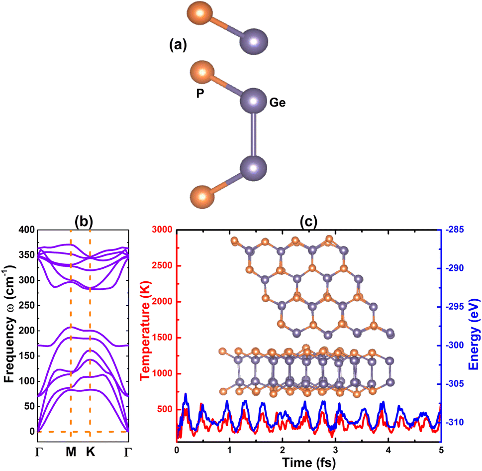
In recent years, IV–V group monolayers in a GaS-like hexagonal structure with double layer configuration have been exploited by several groups because of their stability and semiconductor nature.41,71–74 Herein, the GeP monolayer in hexagonal structure is predicted. Fig. 1a shows the top-view and side-view of a unit cell of a GeP monolayer that contains four atoms (two equivalent Ge atoms and two equivalent P atoms). From the figure, one can see the tetra-layered structure, in which two vertically aligned Ge–Ge dimer atoms are bound to six P atoms. With the hexagonal configuration, the structure is ascribed to P![[6 with combining macron]](https://www.rsc.org/images/entities/char_0036_0304.gif) m2 space group (no. 187), exhibiting D3h symmetry. From the structural relaxation, the following parameters are obtained for the GeP monolayer unit cell: lattice constant a = 3.66 Å, which is in line with previous studies;41 chemical bond lengths dGe–P = 2.37 Å and dGe–Ge = 2.51 Å; interatomic angles ∠PGeP = 101.14° and ∠PGeGe = 116.89°; and total buckling height Δt = 2 × ΔGe–P + ΔGe–Ge = 2 × 1.07 + 2.51 = 4.65 Å. Before investigating the electronic properties of the GeP monolayer, its structural stability is examined as follows: Fig. 1b shows the phonon dispersion curves of the GeP monolayer that exhibit no imaginary frequency in the whole Brillouin zone. The absence of a soft phonon mode asserts that this 2D material is dynamically stable; results of the AIMD simulations are displayed in Fig. 1c. From the figure, one can see that temperature and total energy fluctuate around a fixed value. Moreover, the inset shows that the initial structural geometry is well-preserved. These results indicate that the GeP monolayer is thermally stable; in order to determine the mechanical stability, the Born criteria C11 > 0 and C11 > |C12| should be satisfied for the 2D hexagonal structures.75 Using the stress–strain method, elastic constants C11 = 111.57 N m−1 and C12 = 22.37 N m−1 are obtained for the GeP monolayer. Note that these values follow the mentioned criteria, confirming that the GeP monolayer is mechanically stable, and cohesive energy is defined by:
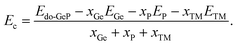
m2 space group (no. 187), exhibiting D3h symmetry. From the structural relaxation, the following parameters are obtained for the GeP monolayer unit cell: lattice constant a = 3.66 Å, which is in line with previous studies;41 chemical bond lengths dGe–P = 2.37 Å and dGe–Ge = 2.51 Å; interatomic angles ∠PGeP = 101.14° and ∠PGeGe = 116.89°; and total buckling height Δt = 2 × ΔGe–P + ΔGe–Ge = 2 × 1.07 + 2.51 = 4.65 Å. Before investigating the electronic properties of the GeP monolayer, its structural stability is examined as follows: Fig. 1b shows the phonon dispersion curves of the GeP monolayer that exhibit no imaginary frequency in the whole Brillouin zone. The absence of a soft phonon mode asserts that this 2D material is dynamically stable; results of the AIMD simulations are displayed in Fig. 1c. From the figure, one can see that temperature and total energy fluctuate around a fixed value. Moreover, the inset shows that the initial structural geometry is well-preserved. These results indicate that the GeP monolayer is thermally stable; in order to determine the mechanical stability, the Born criteria C11 > 0 and C11 > |C12| should be satisfied for the 2D hexagonal structures.75 Using the stress–strain method, elastic constants C11 = 111.57 N m−1 and C12 = 22.37 N m−1 are obtained for the GeP monolayer. Note that these values follow the mentioned criteria, confirming that the GeP monolayer is mechanically stable, and cohesive energy is defined by: 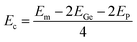 , where Em is the total energy of a GeP unit cell and EGe/EP are the energy of an isolated Ge/P atom. Our calculations provide a negative Ec value of −3.72 eV per atom, which suggests a good structural-chemical stability for the GeP monolayer.
 |
| | Fig. 1 (a) Atomic structure in a unit cell (top-view and side-view), (b) phonon dispersion curves, and (c) fluctuation of temperature and energy during AIMD simulations ((Inset): atomic structure after simulations), of GeP monolayer. | |
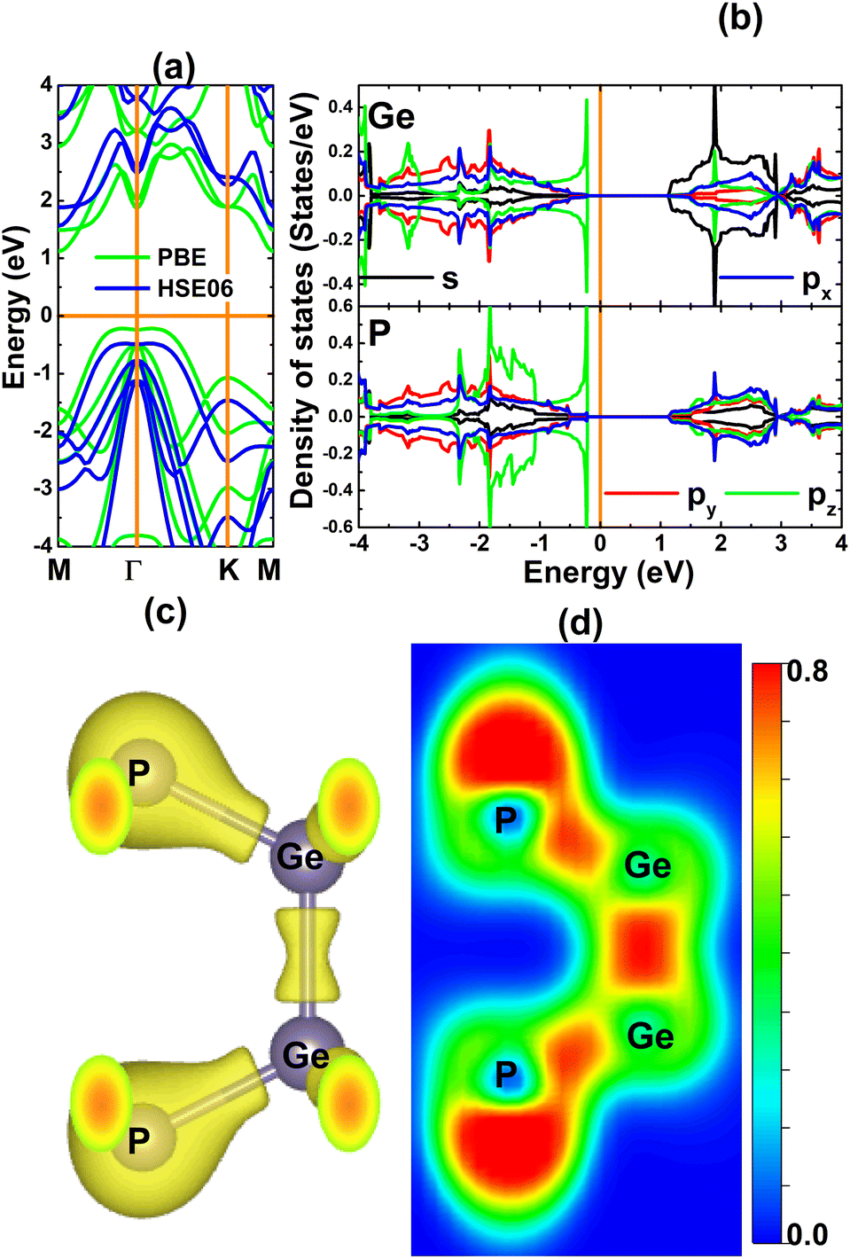
In the following, the electronic properties and chemical bonds of the GeP monolayer are examined. Besides the PBE functional, the hybrid functional HSE06 is also utilized considering its ability to provide a more accurate monolayer band gap – facilitated by 25% fraction of the exact Hartree exchange potential.76 Our spin-polarized calculations demonstrate the absence of intrinsic magnetism in the GeP monolayer, such that zero magnetic moment is obtained. Fig. 2a shows the calculated band structures. Note that the PBE and HSE06 functional yield quite similar band structure profiles that assert the indirect gap semiconductor nature of the GeP monolayer. Herein, the valence band maximum and conduction band minimum take place along the MΓ path and M point, respectively. According to our PBE- and HSE06-based calculations, relatively large energy gaps of 1.34 and 2.04 eV are obtained for the GeP monolayer, respectively. These results are in good agreement with previous calculations,77 suggesting the reliability of our results. Further, the projected density of states (PDOS) spectra are given in Fig. 2b, which assert the contribution from all constituent atoms in constructing the energy diagram. Focusing on the vicinity of the Fermi level, one can see that the low-energy region of the conduction band is formed mainly by the Ge-s state, while the high-energy part of the valence band originates mainly from the electronic hybridization between the Ge-pz and P-pz states. This hybridization suggests that Ge and P atoms are covalently bound. The covalent chemical bond is further confirmed by the charge distribution (Fig. 2c) and electron localization function (Fig. 2d) of the GeP monolayer, in which significant charge is observed in the region between Ge and P atoms to indicate their covalent bond. A similar feature is also noted in the region between Ge atoms, indicating that the Ge–Ge bond is predominantly covalent. However, the difference in electronegativity may cause charge transfer from the Ge atom to P atom, which is also suggested by the directionality of charge towards the P atom in Fig. 2c and d. Therefore, the Bader charge is further analyzed, and the results indicate that each P atom attracts charge of 0.48e from each Ge atom. This feature suggests significant ionic character of the Ge–P chemical bond.
 |
| | Fig. 2 (a) Electronic band structure (horizontal line: the Fermi level is set to 0 eV), (b) projected density of states calculated using the PBE functional (vertical line: the Fermi level is set to 0 eV; positive DOS value: spin-up; negative DOS value: spin-down), (c) charge distribution (iso-surface value: 0.06 e Å−3), and (d) electron localization function of the GeP monolayer. | |
3.2 Effects of Ge vacancies
In this part, the effects of single Ge vacancy (VaGe system) and pair Ge vacancies (pVaGe system) on the GeP monolayer’s electronic and magnetic properties, are investigated. Firstly, the formation energy Ef of vacancies is estimated using the following equation:| | |
Ef = Ede-GeP − EGeP + nGeμGe
| (1) |
where Ede-GeP and EGeP denote total energy of the defected and perfect GeP monolayer, respectively; nGe and μGe are the number of Ge vacancies and chemical potential of the Ge atom, respectively. μGe is calculated from the most stable bulk phase of germanium. Results are listed in Table 1. According to our calculations, additional energy of 3.47 eV is needed to create a single Ge vacancy, while a larger energy of 6.85 eV should be supplied to form a pair of Ge vacancies (corresponding to 3.425 eV for each single vacancy). Then, cohesive energy Ec of the defected GeP systems is calculated to analyze its structural-chemical stability as follows:| |
 | (2) |
Herein, EX and xX are the energy of an isolated atom X (X = Ge or P) and number of atom X in the system, respectively. From Table 1, one can see negative values of −3.66 and −3.61 eV per atom for the VaGe and pVaGe systems, respectively. Negative Ec values suggest that these systems are structural-chemically stable. It is important to mention that the stability of the GeP monolayer is slightly affected by creating Ge vacancies, such that the cohesive energy becomes slightly less negative (that of a perfect GeP monolayer is −3.72 eV per atom).
Table 1 Formation energy Ef (eV per atom), cohesive energy Ec (eV per atom), electronic band gap Eg (eV; spin-up/spin-down; M: metallic), charge transferred from transition metal impurity ΔQ(e), total magnetic moment per unit cell Mt (μB), local magnetic moment of atoms closest to vacancy sites/impurity Ml (μB) of the defected/doped GeP monolayer
| |
Ef |
Ec |
Eg |
ΔQ |
Mt |
Ml |
| VaGe |
3.47 |
−3.66 |
0.64/0.25 |
— |
2.00 |
0.23 |
| pVaGe |
6.85 |
−3.61 |
M/0.19 |
— |
2.02 |
0.13 |
| MnGe |
1.54 |
−3.66 |
1.18/M |
0.65 |
3.00 |
3.57 |
| FeGe |
1.47 |
−3.70 |
0.28/0.98 |
0.42 |
4.00 |
3.30 |
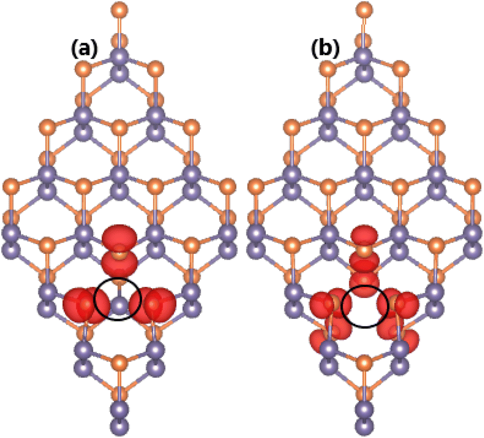
It is found that both types of vacancy lead to significant magnetization of the GeP monolayer, confirmed through analysis of magnetic moments and spin density. According to our calculations, total magnetic moments of 2.00 and 2.02 μB are obtained for the VaGe and pVaGe systems, respectively. The difference in spin-dependent charge distribution is further determined by the illustration of spin density in Fig. 3, in which the unbalanced charge distribution is confirmed by spin iso-surfaces. From the figure, one can see that magnetic properties of both defected GeP systems are produced mainly by P atoms around the vacancy sites. Herein, P atoms in the VaGe and pVaGe systems have local magnetic moments of 0.23 and 0.13 μB, respectively; this can be attributed to the creation of dangling bonds in these P atoms with unbalanced charge distribution between their spin channels. The origin of magnetism is similar to that of the vacancy-doped GaSe monolayer78 that shares the same structure with the GeP monolayer.
 |
| | Fig. 3 Spin density (iso-surface value: 0.005 e Å−3) in GeP monolayer with (a) single Ge vacancy and (b) pair Ge vacancies (vacancy sites are marked). | |
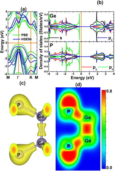
The appearance of magnetism is also reflected in the strong spin polarization of the calculated band structures, which are displayed in Fig. 4. Note that the spin symmetry of the GeP monolayer is broken mostly at the vicinity of the Fermi level when creating Ge vacancies as a consequence of new mid-gap energy branches. Interestingly, the band structure profile implies the diluted magnetic semiconductor nature of the VaGe system, where energy gaps of 0.64 and 0.25 eV are obtained for the spin-up and spin-down state, respectively. The half-metallicity is induced in the GeP monolayer after creating a pair of Ge vacancies. In this case, the spin-up state is metallized, meanwhile the semiconductor character is preserved in the spin-down state with a band gap of 0.19 eV. Since 2D diluted magnetic semiconductor and half-metallic systems can be recommended as prospective candidates for spintronic applications,79,80 the creation of Ge vacancies may be an effective method to functionalize the GeP monolayer towards fabricating spintronic materials.
 |
| | Fig. 4 Spin-polarized band structure calculated with PBE functional (horizontal line: the Fermi level is set to 0 eV) of the GeP monolayer with (a) single Ge vacancy and (b) pair Ge vacancies. | |
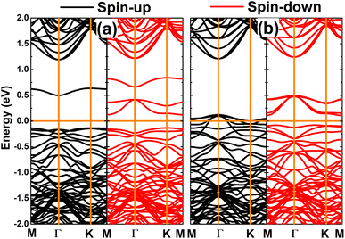
To provide more detail on the electronic and magnetic properties, the PDOS spectra of the atoms closest to vacancies are given in Fig. 5. From the figure, one can see that the mid-gap states of the VaGe system originate mainly from the P-pz state – the low-energy part of the spin-down state (with small contribution from the px and py state), and Ge-s–pz states – high-energy part. The PDOS spectra also suggest that the VaGe system magnetism originates mainly from the P-pz state. Meanwhile, the px,y,z states of the P atoms around the defect sites, are the main contributors of the magnetic properties of the pVaGe system, which have a significant presence around the Fermi level with strong spin polarization resulting in the half-metallicity.
 |
| | Fig. 5 Projected density of states calculated with PBE functional (vertical line: the Fermi level is set to 0 eV; positive DOS value: spin-up; negative DOS value: spin-down) of atoms closest to defect sites in the GeP monolayer with (a) single Ge vacancy and (b) pair Ge vacancies. | |
3.3 Effects of doping with Mn and Fe
Now, the effects of doping with transition metals (TM = Mn − MnGe and Fe − FeGe) on the GeP monolayer’s electronic and magnetic properties are investigated. Firstly, the formation energy Ef of the doped system is calculated using the following expression:| | |
Ef = Edo-GeP − EGeP + μGe − μTM
| (3) |
where Edo-GeP is the total energy of the doped system. Similar to μGe, μTM is calculated from the most stable bulk phase of transition metals. Then, cohesive energy Ec of the doped GeP systems is also computed as follows:| |
 | (4) |
All of the obtained Ef and Ec values are given in Table 1. From the table, it can be seen that additional energy (Ef) of 1.54 and 1.47 eV should be supplied to replace one Ge atom in the GeP monolayer by one Mn or one Fe atom, respectively. Once doping is realised, the Mn- and Fe-doped systems have good structural-chemical stability as suggested by their negative Ec values of −3.66 and −3.70 eV per atom, respectively, which exhibit only slight variation from the −3.72 eV per atom of the bare monolayer.
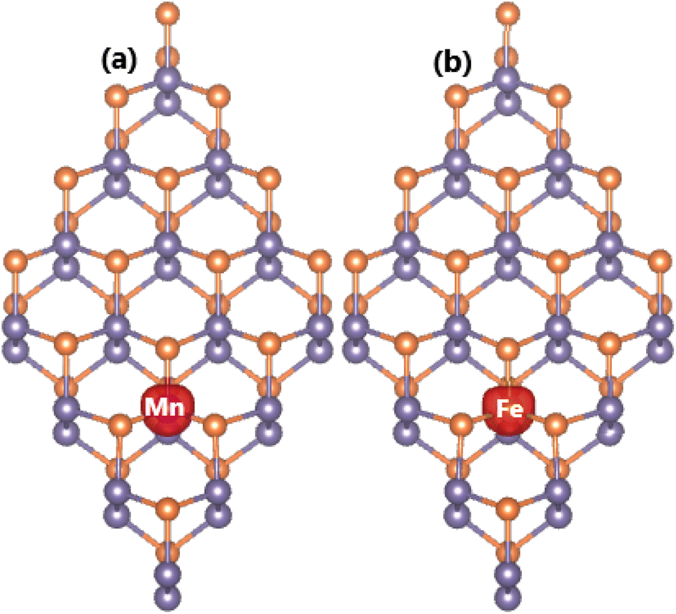
Our spin-polarized calculations demonstrate the significant magnetism induced in the GeP monolayer by doping with transition metals. Fig. 6 illustrates the spin density in the doped systems, where it can be noted that spin iso-surfaces are centred mainly at the TM sites. The spin density profile indicates that Mn and Fe atoms produce mainly the system magnetic properties. Consequently, total magnetic moments of 3.00 and 4.00 μB are obtained for the Mn- and Fe-doped GeP monolayer, respectively. In these cases, Mn and Fe impurities have local magnetic moments of 3.57 and 3.30 μB, respectively. In addition, the charge transfer from TM impurities to the host monolayer is confirmed using Bader charge analysis, which indicates that Mn and Fe impurities lose charge of 0.65 and 0.42e, respectively. Note that the charge loss of Mn and Fe atoms is due to their metallic nature, which is less electronegative than their surrounding P atoms.
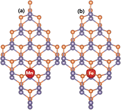 |
| | Fig. 6 Spin density (iso-surface value: 0.02 e Å−3) in GeP monolayer doped with (a) single Mn atom (MnGe system) and (b) single Fe atom (FeGe system). | |
The atomic substitution creates the emergence of feature-rich electronic properties – desirable for spintronic applications – as confirmed by the calculated band structures in Fig. 7. The novel features are regulated by new mid-gap energy branches in both spin channels. Specifically, the Mn-doped GeP monolayer exhibits a semiconductor spin-up state with an energy gap of 1.18 eV and metallic spin-down state. Consequently, this system can be classified as a 2D half-metallic material with perfect spin polarization at the Fermi level. On the contrary, Fe doping induces a diluted magnetic semiconductor nature in the GeP monolayer, where the semiconductor spin-up and spin-down states have an energy gap of 0.28 and 0.98 eV, respectively. These results may introduce new 2D candidates for spintronic applications made by doping the GeP monolayer with Mn and Fe atoms.81
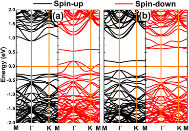 |
| | Fig. 7 Spin-polarized band structure calculated using the PBE functional (horizontal line: the Fermi level is set to 0 eV) of the GeP monolayer doped with (a) single Mn atom (MnGe system) and (b) single Fe atom (FeGe system). | |
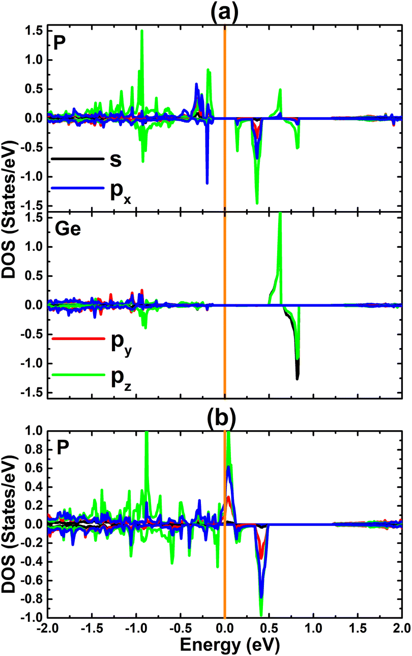
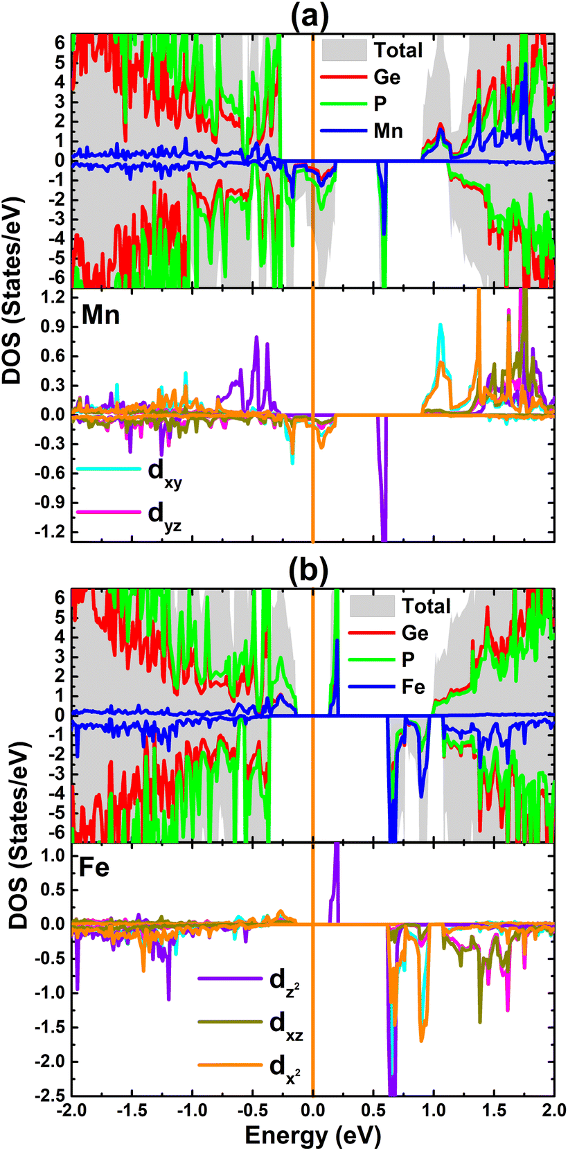
The total and atom-decomposed density of states of the MnGe and FeGe systems are given in Fig. 8. Note that the Mn and Fe atoms contribute mainly to the mid-gap states and to the conduction band, where the contribution from the host Ge and P atoms is also observed. Since TM impurities produce the main system magnetism, their PDOS spectra are also given to analyze the orbital-decomposed contribution. In the energy range considered, from −2 to 2 eV, there is the main contribution from the 3d orbital that originates mainly from the mid-gap energy states, whereas that from other s and p orbitals is negligible. The spin-down metallic character of the MnGe system can be attributed mainly to the Mn-dxy and Mn-dx2 states. Moreover, the dz2 state of both TM impurities may significantly participate in regulating the ground state electronic nature of the doped systems, considering their important presence around the Fermi level. Most importantly, electronic and magnetic properties are produced mainly by the 3d electrons of the Mn and Fe atoms as suggested by the strong spin polarization of the 3d orbital.
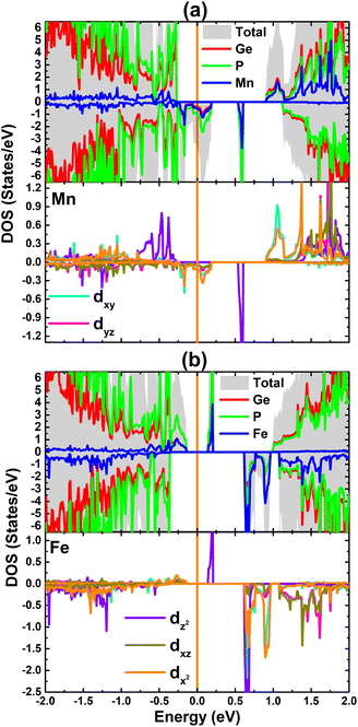 |
| | Fig. 8 Total density of states, atom-decomposed density of states, and projected density of states of transition metals calculated with PBE functional (vertical line: the Fermi level is set to 0 eV; positive DOS value: spin-up; negative DOS value: spin-down) of transition metal impurities in GeP monolayer doped with (a) single Mn atom (MnGe system) and (b) single Fe atom (FeGe system). | |
3.4 Spin alignment in Mn- and Fe-doped GeP monolayer
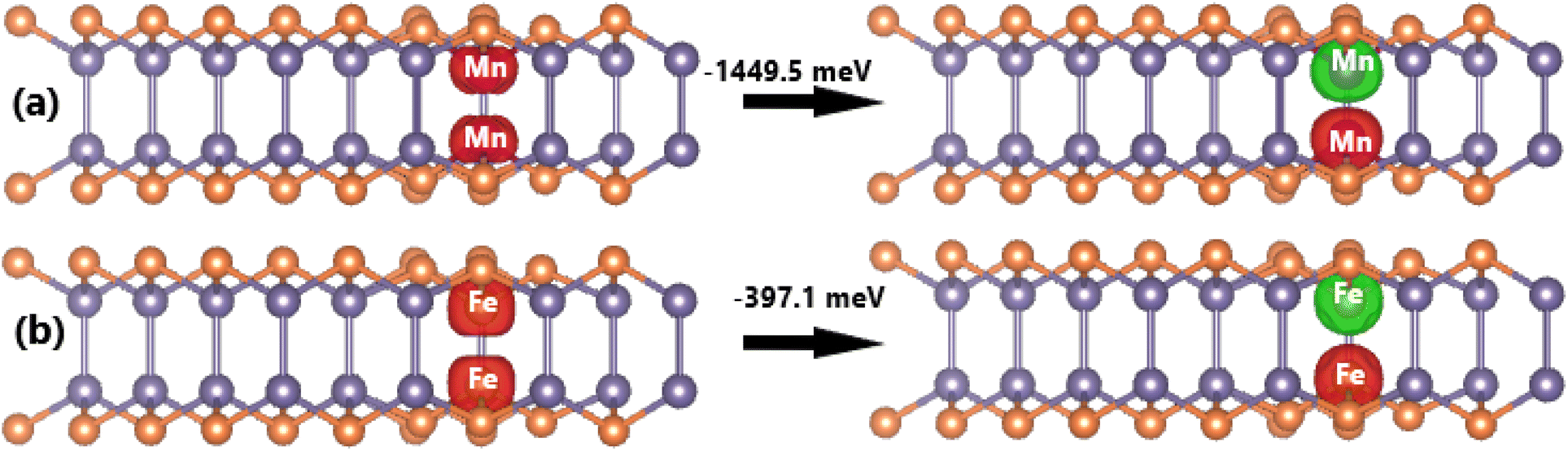
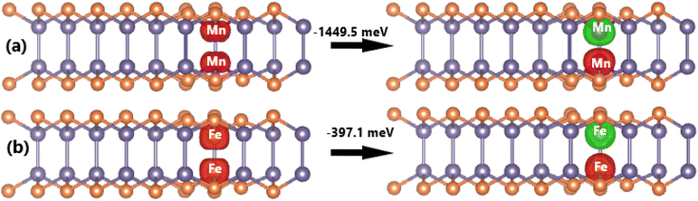
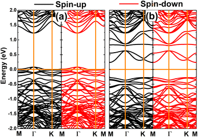
Now, the spin orientation in Mn- and Fe-doped GeP monolayer and its effects on the electronic properties are investigated. Firstly, the cases of doping with pair transition metals (pMnGe and pFeGe systems) are studied. According to our calculations, the antiferromagnetic state with antiparallel spin orientation is energetically favorable over the ferromagnetic state with parallel spin orientation. The obtained differences in energy are 1449.5 and 397.1 meV for pMn- and pFe-doped GeP systems, respectively (see Fig. 9). It is important to mention that the differences in energy are large, which derive from the Pauli expulsion between the 3d electrons of the transition metals that do not have any host atom located between them.82 According to our calculations, additional energies of 3.66 and 3.16 eV are required to realize the doping with pair Mn atoms and pair Fe atoms, respectively. Moreover, pMnGe and pFeGe systems have negative Ec values of −3.60 and −3.67 eV per atom, respectively, suggesting their good structural-chemical stability. In the antiferromagnetic state, the magnetism originates mainly from transition metals. Since two impurities are located at equivalent sites, they have equal (absolute) magnetic moments with opposite signs. Consequently, a zero total magnetic moment is obtained. Moreover, the band structures exhibit no spin polarization, as displayed in Fig. 10. The figure shows that the pMnGe system is an antiferromagnetic metallic system, meanwhile the antiferromagnetic semiconductor nature is obtained by doping with a pair of Fe atoms (pFeGe system).
 |
| | Fig. 9 Spin density (iso-surface value: 0.02 e Å−3; red surface: positive spin value; green surface: negative spin value) and energy of magnetic state transition in (a) pMn- and (b) pFe-doped GeP monolayer. | |
 |
| | Fig. 10 Spin-polarized band structure calculated with PBE functional (horizontal line: the Fermi level is set to 0 eV) of (a) pMn- and (b) pFe-doped GeP monolayer. | |
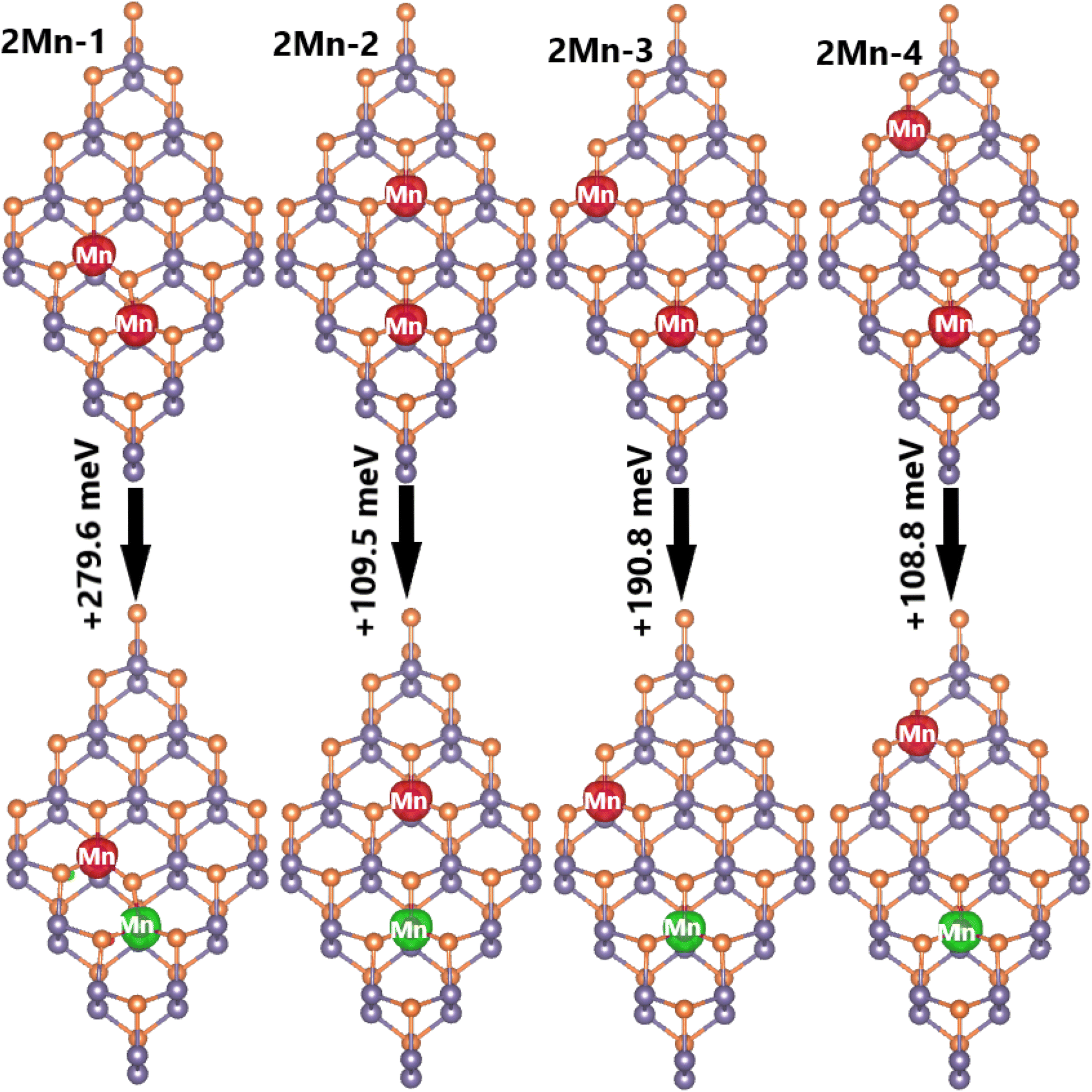
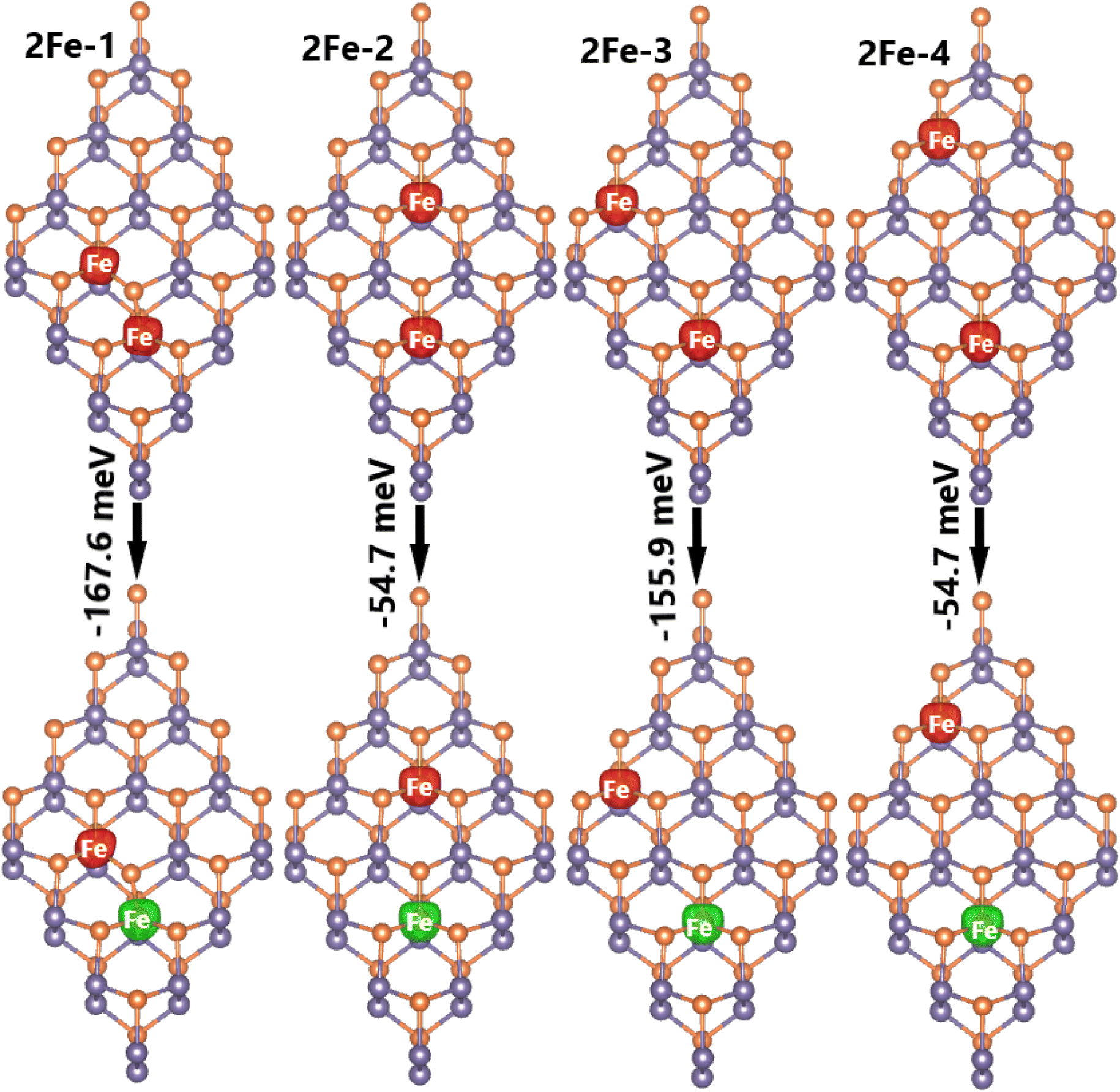
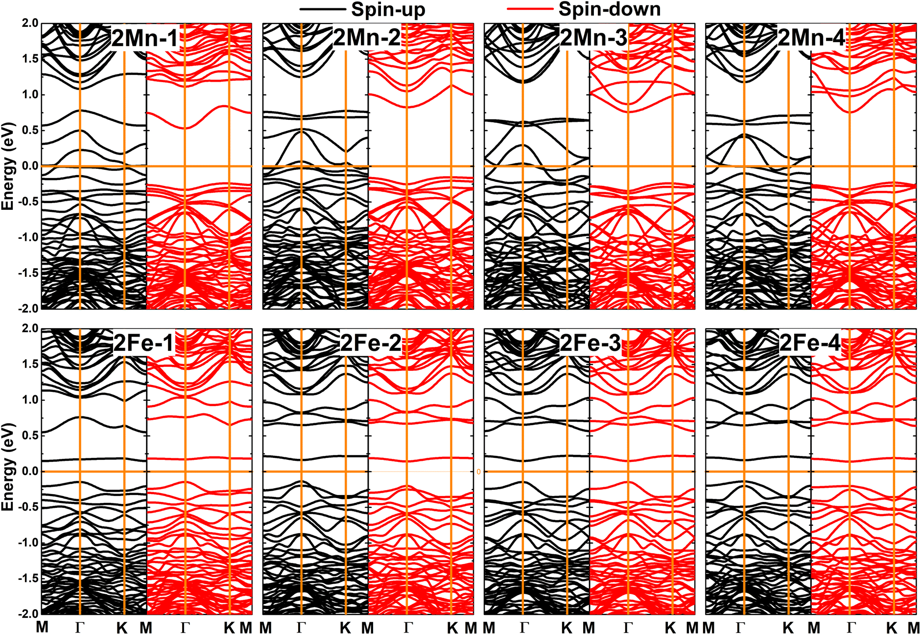
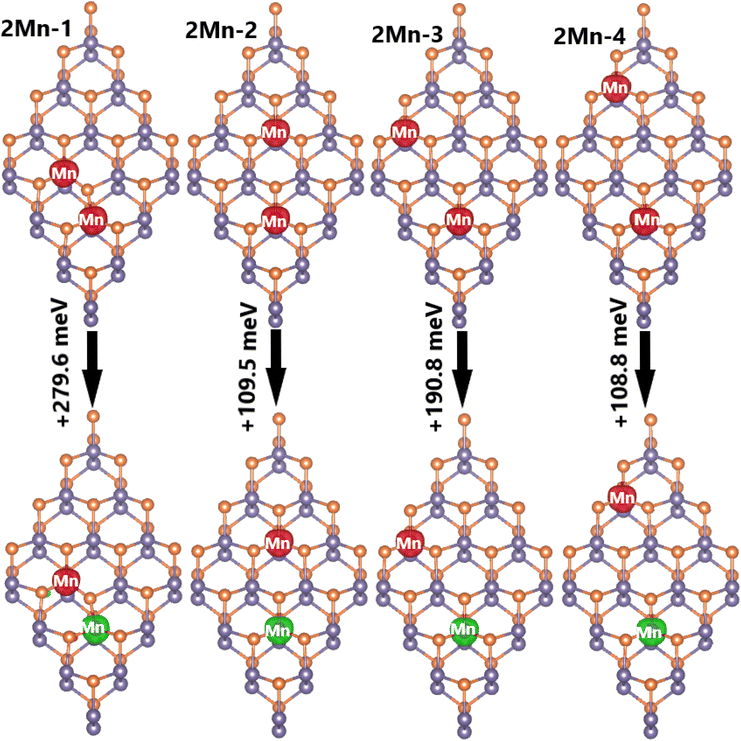
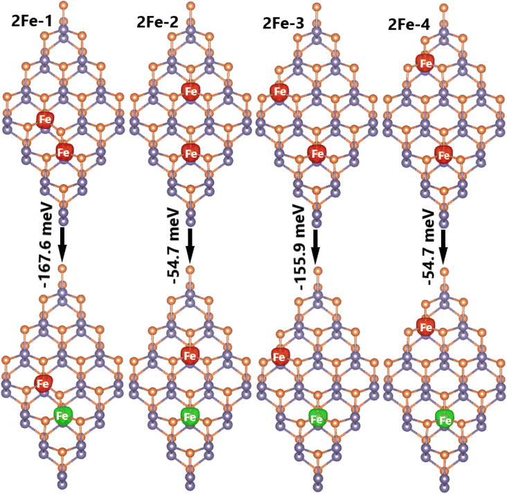
Now, doping at Ge sublattices at the same atomic sublayer is studied, where different interatomic distances between two transition metal atoms are considered. Herein, the systems are denoted by 2TM-n (n = 1 to 4, which increases with increasing distance between the transition metal atoms). It is found that the ferromagnetic state with parallel spin orientation is energetically favorable for Mn-doped systems, exhibiting difference in energy between 108.8 and 279.6 meV smaller than the antiferromagnetic state, as illustrated in Fig. 11. In contrast, the antiferromagnetic state with antiparallel spin orientation is stable in Fe-doped systems considering its lower energy in comparison with the ferromagnetic state (the difference in energy is between 54.7 and 167.6 meV higher, see Fig. 12). These results indicate that Coulomb repulsion interactions are dominant in 2Mn-n systems, meanwhile Pauli expulsion determines the antiferromagnetic state of 2Fe-n systems. Moreover, the spin surfaces are concentrated mainly at transition metal sites, indicating their key role in producing the system magnetism. In Table 2, one can see Ef values between 2.94 and 3.25 eV for 2Mn-n systems, while smaller values between 2.78 and 2.92 eV are obtained for 2Fe-n systems. It is important to mention that 2TM-3 systems are energetically the most favorable because they have the smallest Ef values. In addition, all the studied systems are proven to be structural-chemically stable considering their negative Ec values. Further, the electronic band structures are displayed in Fig. 13, which show two different features: all the Mn-doped GeP systems exhibit the ferromagnetic half-metallicity generated by the metallic spin-up state and semiconductor spin-down state. The spin-down energy gaps of 0.77, 0.98, 1.00, and 0.98 eV are obtained for 2Mn-1, 2Mn-2, 2Mn-3, and 2Mn-4 systems, respectively; whereas all the Fe-doped GeP systems exhibit antiferromagnetic semiconductor nature. In these cases, the spin-up/spin-down band gaps of 0.29/0.32, 0.30/0.34, 0.29/0.29, and 0.30/0.34 eV are obtained for 2Fe-1, 2Fe-2, 2Fe-3, and 2Fe-4, respectively.
 |
| | Fig. 11 Spin density (iso-surface value: 0.02 e Å−3; red surface: positive spin value; green surface: negative spin value) and energy of magnetic transition in 2Mn-n (n = 1, 2, 3, and 4) systems. | |
 |
| | Fig. 12 Spin density (iso-surface value: 0.02 e Å−3; red surface: positive spin value; green surface: negative spin value) and energy of magnetic transition in 2Fe-n (n = 1, 2, 3, and 4) systems. | |
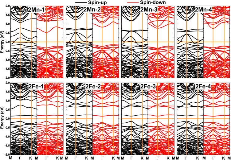 |
| | Fig. 13 Spin-polarized band structure calculated with PBE functional (horizontal line: the Fermi level is set to 0 eV) of 2Mn- and 2Fe-doped GeP monolayers with different distances between transition metal impurities. | |
Table 2 Interatomic distance between impurities dTM–TM (Å), formation energy Ef (eV per atom), cohesive energy Ec (eV per atom), electronic band gap Eg (eV; spin-up/spin-down; M: metallic), total magnetic moment per unit cell Mt (μB), and local magnetic moment of impurities MTMs (μB) of the doped GeP monolayer
| |
dTM–TM |
Ef |
Ec |
Eg |
Mt |
MTMs |
| pMnGe |
1.89 |
3.66 |
−3.60 |
M/M |
0.00 |
3.39/−3.39 |
| 2Mn-1 |
3.92 |
3.25 |
−3.61 |
M/0.77 |
6.00 |
3.54/3.54 |
| 2Mn-2 |
6.27 |
3.08 |
−3.61 |
M/0.98 |
6.00 |
3.56/3.56 |
| 2Mn-3 |
7.33 |
2.94 |
−3.62 |
M/1.00 |
6.00 |
3.56/3.56 |
| 2Mn-4 |
9.75 |
3.08 |
−3.61 |
M/0.98 |
6.00 |
3.56/3.56 |
| pFeGe |
2.13 |
3.16 |
−3.67 |
0.51/0.51 |
0.00 |
3.19/−3.19 |
| 2Fe-1 |
3.83 |
2.92 |
−3.68 |
0.29/0.32 |
0.00 |
3.05/−3.05 |
| 2Fe-2 |
6.33 |
2.92 |
−3.68 |
0.30/0.34 |
0.00 |
3.28/−3.28 |
| 2Fe-3 |
7.33 |
2.78 |
−3.68 |
0.29/0.29 |
0.00 |
3.25/−3.25 |
| 2Fe-4 |
9.71 |
2.92 |
−3.68 |
0.30/0.34 |
0.00 |
3.28/−3.28 |
4. Conclusions
In summary, the electronic and magnetic properties of the GeP monolayer under the effects of Ge vacancies and doping with transition metals (Mn and Fe), have been systematically investigated using first-principles calculations. The calculated phonon diagrams and elastic constants, as well as AIMD simulations confirm the good stability of the pristine GeP monolayer. It is found that the Ge–P chemical bond is a mix of covalent and ionic characters, while the Ge–Ge bond is predominantly covalent. Moreover, the spin-polarized calculations demonstrate its semiconductor character without intrinsic magnetism. Creating Ge vacancies and doping with transition metals is proposed as an efficient method to induce magnetism in the GeP monolayer with feature-rich electronic properties towards spintronic applications. The magnetic properties of the defected systems are produced mainly by the px,y,x of the P atoms closest to vacancy sites, while the 3d electrons of Mn and Fe impurities originate mainly from the magnetism of the doped systems. Further investigations assert the antiferromagnetic state in the GeP monolayer when doping with pair transition metals. Herein, pMnGe and pFeGe are antiferromagnetic metallic and semiconductor 2D materials, respectively. Moreover, the ferromagnetic half-metallicity is also confirmed for Mn-doped GeP systems, where the parallel spin orientation exhibits lower energy than the antiparallel orientation regardless of the distance between impurities. In contrast, all Fe-doped GeP systems are antiferromagnetic diluted magnetic 2D materials provided that the antiferromagnetic state is energetically more favorable than the ferromagnetic state. Our study may create a reliable way to realize new ferromagnetic/antiferromagnetic 2D materials made from the GeP monolayer, which may be recommended as promising candidates for nano-spintronics.
Data availability
Data related to this study are available upon reasonable request.
Conflicts of interest
The authors declare that they have no known competing financial interests or personal relationships that could have appeared to influence the work reported in this paper.
Acknowledgements
Calculations were performed at the DGCTIC-UNAM Supercomputing Center (projects LANCAD-UNAM-DGTIC-368) and the high-performance computing cluster (HPCC) of Thu Dau Mot University (TDMU). D. M. Hoat expresses his gratitude to all the valuable support from Duy Tan University, which is going to celebrate its 30th anniversary of establishment (Nov. 11, 1994–Nov. 11, 2024) towards “Integral, Sustainable and Stable Development”.
References
- K. S. Novoselov, A. K. Geim, S. V. Morozov, D.-e. Jiang, Y. Zhang, S. V. Dubonos, I. V. Grigorieva and A. A. Firsov, Electric field effect in atomically thin carbon films, Science, 2004, 306(5696), 666–669 CrossRef CAS PubMed
 .
. - K. Novoselov, S. Morozov, T. Mohinddin, L. Ponomarenko, D. C. Elias, R. Yang, I. Barbolina, P. Blake, T. Booth and D. Jiang, et al., Electronic properties of graphene, Phys. Status Solidi B, 2007, 244(11), 4106–4111 CrossRef CAS .
- S. Eigler, C. Dotzer and A. Hirsch, Visualization of defect densities in reduced graphene oxide, Carbon, 2012, 50(10), 3666–3673 CrossRef CAS .
- Y.-W. Son, M. L. Cohen and S. G. Louie, Energy gaps in graphene nanoribbons, Phys. Rev. Lett., 2006, 97(21), 216803 CrossRef PubMed .
- M. Y. Han, B. Özyilmaz, Y. Zhang and P. Kim, Energy band-gap engineering of graphene nanoribbons, Phys. Rev. Lett., 2007, 98(20), 206805 CrossRef .
- J. Zhou, M. M. Wu, X. Zhou and Q. Sun, Tuning electronic and magnetic properties of graphene by surface modification, Appl. Phys. Lett., 2009, 95(10), 103108 CrossRef .
- T. Kuila, S. Bose, A. K. Mishra, P. Khanra, N. H. Kim and J. H. Lee, Chemical functionalization of graphene and its applications, Prog. Mater. Sci., 2012, 57(7), 1061–1105 CrossRef CAS .
- L. Tao, E. Cinquanta, D. Chiappe, C. Grazianetti, M. Fanciulli, M. Dubey, A. Molle and D. Akinwande, Silicene field-effect transistors operating at room temperature, Nat. Nanotechnol., 2015, 10(3), 227–231 CrossRef CAS .
- A. Acun, L. Zhang, P. Bampoulis, M. v. Farmanbar, A. van Houselt, A. Rudenko, M. Lingenfelder, G. Brocks, B. Poelsema and M. Katsnelson, et al., Germanene: the germanium analogue of graphene, J. Phys.: Condens. Matter, 2015, 27(44), 443002 CrossRef CAS PubMed .
- L. Li, Y. Yu, G. J. Ye, Q. Ge, X. Ou, H. Wu, D. Feng, X. H. Chen and Y. Zhang, Black phosphorus field-effect transistors, Nat. Nanotechnol., 2014, 9(5), 372–377 CrossRef CAS .
- W. Zhang, H. Enriquez, Y. Tong, A. Bendounan, A. Kara, A. P. Seitsonen, A. J. Mayne, G. Dujardin and H. Oughaddou, Epitaxial synthesis of blue phosphorene, Small, 2018, 14(51), 1804066 CrossRef .
- K. K. Kim, A. Hsu, X. Jia, S. M. Kim, Y. Shi, M. Hofmann, D. Nezich, J. F. Rodriguez-Nieva, M. Dresselhaus and T. Palacios, et al., Synthesis of monolayer hexagonal boron nitride on Cu foil using chemical vapor deposition, Nano Lett., 2012, 12(1), 161–166 CrossRef .
- Y. Stehle, H. M. Meyer III, R. R. Unocic, M. Kidder, G. Polizos, P. G. Datskos, R. Jackson, S. N. Smirnov and I. V. Vlassiouk, Synthesis of hexagonal boron nitride monolayer: control of nucleation and crystal morphology, Chem. Mater., 2015, 27(23), 8041–8047 CrossRef CAS .
- S. A. Han, R. Bhatia and S.-W. Kim, Synthesis, properties and potential applications of two-dimensional transition metal dichalcogenides, Nano Convergence, 2015, 2, 1–14 CrossRef .
- Y. Shi, H. Li and L.-J. Li, Recent advances in controlled synthesis of two-dimensional transition metal dichalcogenides via vapour deposition techniques, Chem. Soc. Rev., 2015, 44(9), 2744–2756 RSC .
- C. Zhang, Y. Ma, X. Zhang, S. Abdolhosseinzadeh, H. Sheng, W. Lan, A. Pakdel, J. Heier and F. Nüesch, Two-dimensional transition metal carbides and nitrides (MXenes): synthesis, properties, and electrochemical energy storage applications, Energy Environ. Mater., 2020, 3(1), 29–55 CrossRef CAS .
- A. VahidMohammadi, J. Rosen and Y. Gogotsi, The world of two-dimensional carbides and nitrides (MXenes), Science, 2021, 372(6547), eabf1581 CrossRef CAS PubMed .
- L. Tang, X. Meng, D. Deng and X. Bao, Confinement catalysis with 2D materials for energy conversion, Adv. Mater., 2019, 31(50), 1901996 CrossRef CAS .
- T. A. Shifa, F. Wang, Y. Liu and J. He, Heterostructures based on 2D materials: a versatile platform for efficient catalysis, Adv. Mater., 2019, 31(45), 1804828 CrossRef CAS .
- S. Das, D. Pandey, J. Thomas and T. Roy, The role of graphene and other 2D materials in solar photovoltaics, Adv. Mater., 2019, 31(1), 1802722 CrossRef PubMed .
- Z. Liu, S. P. Lau and F. Yan, Functionalized graphene and other two-dimensional materials for photovoltaic devices: device design and processing, Chem. Soc. Rev., 2015, 44(15), 5638–5679 RSC .
- J. An, X. Zhao, Y. Zhang, M. Liu, J. Yuan, X. Sun, Z. Zhang, B. Wang, S. Li and D. Li, Perspectives of 2D materials for optoelectronic integration, Adv. Funct. Mater., 2022, 32(14), 2110119 CrossRef CAS .
- J. Shim, H.-Y. Park, D.-H. Kang, J.-O. Kim, S.-H. Jo, Y. Park and J.-H. Park, Electronic and optoelectronic devices based on two-dimensional materials: From fabrication to application, Adv. Electron. Mater., 2017, 3(4), 1600364 CrossRef .
- R. Kurapati, K. Kostarelos, M. Prato and A. Bianco, Biomedical uses for 2D materials beyond graphene: current advances and challenges ahead, Adv. Mater., 2016, 28(29), 6052–6074 CrossRef CAS .
- T. Hu, X. Mei, Y. Wang, X. Weng, R. Liang and M. Wei, Two-dimensional nanomaterials: fascinating materials in biomedical field, Sci. Bull., 2019, 64(22), 1707–1727 CrossRef CAS PubMed .
- R. Rojaee and R. Shahbazian-Yassar, Two-dimensional materials to address the lithium battery challenges, ACS Nano, 2020, 14(3), 2628–2658 CrossRef CAS .
- N. Deng, Y. Feng, G. Wang, X. Wang, L. Wang, Q. Li, L. Zhang, W. Kang, B. Cheng and Y. Liu, Rational structure designs of 2D materials and their applications toward advanced lithium-sulfur battery and lithium-selenium battery, Chem. Eng. J., 2020, 401, 125976 CrossRef CAS .
- E. C. Ahn, 2D materials for spintronic devices, npj 2D Mater. Appl., 2020, 4(1), 17 CrossRef CAS .
- Y. Liu, C. Zeng, J. Zhong, J. Ding, Z. M. Wang and Z. Liu, Spintronics in two-dimensional materials, Nano–Micro Lett., 2020, 12, 1–26 CrossRef .
- A. Nijamudheen, R. Bhattacharjee, S. Choudhury and A. Datta, Electronic and chemical properties of germanene: the crucial role of buckling, J. Phys. Chem. C, 2015, 119(7), 3802–3809 CrossRef CAS .
- H. Liu, A. T. Neal, Z. Zhu, Z. Luo, X. Xu, D. Tománek and P. D. Ye, Phosphorene: an unexplored 2D semiconductor with a high hole mobility, ACS Nano, 2014, 8(4), 4033–4041 CrossRef CAS PubMed .
- B. Mortazavi and T. Rabczuk, Anisotropic mechanical properties and strain tuneable band-gap in single-layer SiP, SiAs, GeP and GeAs, Phys. E., 2018, 103, 273–278 CrossRef CAS .
- J. Sun and J. Leng, The mechanical flexibility, electronic structure and carrier mobility of monolayer GeP: A first principles study, Phys. Lett. A, 2019, 383(27), 125856 CrossRef CAS .
- L. Li, W. Wang, P. Gong, X. Zhu, B. Deng, X. Shi, G. Gao, H. Li and T. Zhai, 2D GeP: an unexploited low-symmetry semiconductor with strong in-plane anisotropy, Adv. Mater., 2018, 30(14), 1706771 CrossRef .
- F. Yang, J. Hong, J. Hao, S. Zhang, G. Liang, J. Long, Y. Liu, N. Liu, W. K. Pang and J. Chen, et al., Ultrathin few-layer GeP nanosheets via lithiation-assisted chemical exfoliation and their application in sodium storage, Adv. Energy Mater., 2020, 10(14), 1903826 CrossRef CAS .
- E. Jiang, X. Zhu, T. Ouyang, C. Tang, J. Li, C. He, C. Zhang and J. Zhong, The thermoelectric properties of monolayer SiP and GeP from first-principles calculations, J. Appl. Phys., 2019, 126(18), 185106 CrossRef .
- A. Lou, Q.-B. Liu and H.-H. Fu, Enhanced thermoelectric performance by lone-pair electrons and bond anharmonicity in the two-dimensional Ge2Y2 family of materials with Y= N, P, As, or Sb, Phys. Rev. B, 2022, 105(7), 075431 CrossRef CAS .
- C. Niu, T. Lan, D. Wang, J. Pan, J. Chu, C. Wang, H. Yuan, A. Yang, X. Wang and M. Rong, Tunable adsorption behavior of small molecule on GeP monolayer by applied strain and electric field, Appl. Surf. Sci., 2020, 520, 146257 CrossRef CAS .
- D. Wang, T. Lan, A. Yang, J. Pan, J. Chu, H. Yuan, Y. Li, X. Wang and M. Rong, SF6 decomposition gas sensor based on GeP monolayer: A first-principle study, IEEE Sensor. J., 2020, 20(16), 8997–9003 CAS .
- F. Shojaei and H. S. Kang, Electronic structure of the germanium phosphide monolayer and Li-diffusion in its bilayer, Phys. Chem. Chem. Phys., 2016, 18(47), 32458–32465 RSC .
- N. Niasadegh, M. Naseri and S. Rezaee, Structural, electronic and optical properties of GeX (X= N, P and As) monolayer: under stress and strain conditions, Opt. Quantum Electron., 2021, 53(9), 502 CrossRef CAS .
- J. Zhang, G. Yang, J. Tian, Z. Wang, Y. Tang and D. Ma, Effect of atom adsorption on the electronic, magnetic, and optical properties of the GeP monolayer: A first-principle study, Appl. Surf. Sci., 2019, 475, 863–872 CrossRef CAS .
- A. Hirohata, K. Yamada, Y. Nakatani, I.-L. Prejbeanu, B. Diény, P. Pirro and B. Hillebrands, Review on spintronics: Principles and device applications, J. Magn. Magn. Mater., 2020, 509, 166711 CrossRef CAS .
- T. Dietl and H. Ohno, Dilute ferromagnetic semiconductors: Physics and spintronic structures, Rev. Mod. Phys., 2014, 86(1), 187–251 CrossRef CAS .
- B. Huang, G. Clark, E. Navarro-Moratalla, D. R. Klein, R. Cheng, K. L. Seyler, D. Zhong, E. Schmidgall, M. A. McGuire and D. H. Cobden, et al., Layer-dependent ferromagnetism in a van der Waals crystal down to the monolayer limit, Nature, 2017, 546(7657), 270–273 CrossRef CAS .
- C. Gong, L. Li, Z. Li, H. Ji, A. Stern, Y. Xia, T. Cao, W. Bao, C. Wang and Y. Wang, etal., Discovery of intrinsic ferromagnetism in two-dimensional van der Waals crystals, Nature, 2017, 546(7657), 265–269 CrossRef CAS PubMed .
- H. Wu, W. Zhang, L. Yang, J. Wang, J. Li, L. Li, Y. Gao, L. Zhang, J. Du and H. Shu, et al., Strong intrinsic room-temperature ferromagnetism in freestanding non-van der Waals ultrathin 2D crystals, Nat. Commun., 2021, 12(1), 5688 CrossRef CAS PubMed .
- J. J. Palacios, J. Fernández-Rossier and L. Brey, Vacancy-induced magnetism in graphene and graphene ribbons, Phys. Rev. B: Condens. Matter Mater. Phys., 2008, 77(19), 195428 CrossRef .
- H. Zheng, B. Yang, D. Wang, R. Han, X. Du and Y. Yan, Tuning magnetism of monolayer MoS2 by doping vacancy and applying strain, Appl. Phys. Lett., 2014, 104(13), 132403 CrossRef .
- R. Faccio and A. W. Mombru, Magnetism in multivacancy graphene systems, J. Phys.: Condens. Matter, 2012, 24(37), 375304 CrossRef .
- A. Avsar, C.-Y. Cheon, M. Pizzochero, M. Tripathi, A. Ciarrocchi, O. V. Yazyev and A. Kis, Probing magnetism in atomically thin semiconducting PtSe2, Nat. Commun., 2020, 11(1), 4806 CrossRef CAS PubMed .
- O. Dyck, L. Zhang, M. Yoon, J. L. Swett, D. Hensley, C. Zhang, P. D. Rack, J. D. Fowlkes, A. R. Lupini and S. Jesse, Doping transition-metal atoms in graphene for atomic-scale tailoring of electronic, magnetic, and quantum topological properties, Carbon, 2021, 173, 205–214 CrossRef CAS .
- D. Shen, B. Zhao, Z. Zhang, H. Zhang, X. Yang, Z. Huang, B. Li, R. Song, Y. Jin and R. Wu, et al., Synthesis of group VIII magnetic transition-metal-doped monolayer MoSe2, ACS Nano, 2022, 16(7), 10623–10631 CrossRef CAS PubMed .
- J. Zhou, J. Lin, H. Sims, C. Jiang, C. Cong, J. A. Brehm, Z. Zhang, L. Niu, Y. Chen and Y. Zhou, et al., Synthesis of Co-doped MoS2 monolayers with enhanced valley splitting, Adv. Mater., 2020, 32(11), 1906536 CrossRef CAS PubMed .
- J. Ren, H. Zhang and X. Cheng, Electronic and magnetic properties of all 3d transition-metal-doped ZnO monolayers, Int. J. Quantum Chem., 2013, 113(19), 2243–2250 CrossRef CAS .
- W. Kohn and L. J. Sham, Self-consistent equations including exchange and correlation effects, Phys. Rev., 1965, 140(4A), A1133 CrossRef .
- G. Kresse and J. Furthmüller, Efficiency of ab initio total energy calculations for metals and semiconductors using a plane-wave basis set, Comput. Mater. Sci., 1996, 6(1), 15–50 CrossRef CAS .
- G. Kresse and J. Furthmüller, Efficient iterative schemes for ab initio total-energy calculations using a plane-wave basis set, Phys. Rev. B: Condens. Matter, 1996, 54(16), 11169 CrossRef CAS PubMed .
- J. P. Perdew, K. Burke and M. Ernzerhof, Generalized gradient approximation made simple, Phys. Rev. Lett., 1996, 77(18), 3865 CrossRef CAS .
- S. L. Dudarev, G. A. Botton, S. Y. Savrasov, C. Humphreys and A. P. Sutton, Electron-energy-loss spectra and the structural stability of nickel oxide: An LSDA+U study, Phys. Rev. B: Condens. Matter, 1998, 57(3), 1505 CrossRef CAS .
- Y. Wang, S. Li and J. Yi, Transition metal-doped tin monoxide monolayer: a first-principles study, J. Phys. Chem. C, 2018, 122(8), 4651–4661 CrossRef CAS .
- H. A. Huy, D. K. Nguyen, R. Ponce-Pérez, J. Guerrero-Sanchez and D. Hoat, Electronic and magnetic properties of snc monolayer doped with 3d transition metals: a first-principles study, Mater. Today Commun., 2023, 36, 106511 CrossRef CAS .
- S. Grimme, J. Antony, S. Ehrlich and H. Krieg, A consistent and accurate ab initio parametrization of density functional dispersion correction (DFT-D) for the 94 elements H-Pu, J. Chem. Phys., 2010, 132(15), 154104 CrossRef .
- H. J. Monkhorst and J. D. Pack, Special points for Brillouin-zone integrations, Phys. Rev. B: Solid State, 1976, 13(12), 5188 CrossRef .
- K. Momma and F. Izumi, VESTA3 for three-dimensional visualization of crystal, volumetric and morphology data, J. Appl. Crystallogr., 2011, 44(6), 1272–1276 CrossRef CAS .
- W. Tang, E. Sanville and G. Henkelman, A grid-based Bader analysis algorithm without lattice bias, J. Phys.: Condens. Matter, 2009, 21(8), 084204 CrossRef CAS PubMed .
- M. Yu and D. R. Trinkle, Accurate and efficient algorithm for Bader charge integration, J. Chem. Phys., 2011, 134(6), 064111 CrossRef PubMed .
- A. Togo, L. Chaput, T. Tadano and I. Tanaka, Implementation strategies in phonopy and phono3py, J. Phys.: Condens. Matter, 2023, 35(35), 353001 CrossRef CAS .
- W. G. Hoover, Canonical dynamics: Equilibrium phase-space distributions, Phys. Rev. A: At., Mol., Opt. Phys., 1985, 31(3), 1695 CrossRef .
- S. Nosé, A unified formulation of the constant temperature molecular dynamics methods, J. Chem. Phys., 1984, 81(1), 511–519 CrossRef .
- J. Wu, J.-H. Li and Y.-X. Yu, A theoretical analysis on the oxidation and water dissociation resistance on group-IV phosphide monolayers, ChemPhysChem, 2020, 21(22), 2539–2549 CrossRef CAS .
- D. H. Ozbey, M. J. Varjovi, G. Ö. Sargın, H. Sevinçli and E. Durgun, Structural, electronic, vibrational, and thermoelectric properties of Janus Ge2PX (X= N, As, Sb, and Bi) monolayers, Phys. Rev. B, 2024, 110(3), 035411 CrossRef CAS .
- H. T. P. Thuy, V. Van On, R. Ponce-Pérez, J. Guerrero-Sanchez and D. Hoat, Synergistic effects of vacancy and doping at ge sublattices on the electronic and magnetic properties of new Janus Ge2PAs monolayer, Mater. Sci. Semicond. Process., 2024, 184, 108826 CrossRef .
- C. V. Ha, R. Ponce-Perez, J. Guerrero-Sanchez and D. M. Hoat, Point defects in hexagonal SiP monolayer: A systematic investigation on the electronic and magnetic properties, Adv. Theory Simul., 2024, 7(6), 2400320 CrossRef CAS .
- F. Mouhat and F.-X. Coudert, Necessary and sufficient elastic stability conditions in various crystal systems, Phys. Rev. B: Condens. Matter Mater. Phys., 2014, 90(22), 224104 CrossRef .
- A. V. Krukau, O. A. Vydrov, A. F. Izmaylov and G. E. Scuseria, Influence of the exchange screening parameter on the performance of screened hybrid functionals, J. Chem. Phys., 2006, 125(22), 224106 CrossRef .
- B. Özdamar, G. Özbal, M. N. Çınar, K. Sevim, G. Kurt, B. Kaya and H. Sevinçli, Structural, vibrational, and electronic properties of single-layer hexagonal crystals of group IV and V elements, Phys. Rev. B, 2018, 98(4), 045431 CrossRef .
- L. Ao, H. Xiao, X. Xiang, S. Li, K. Liu, H. Huang and X. Zu, Functionalization of a GaSe monolayer by vacancy and chemical element doping, Phys. Chem. Chem. Phys., 2015, 17(16), 10737–10748 RSC .
- X. Li and J. Yang, First-principles design of spintronics materials, Natl. Sci. Rev., 2016, 3(3), 365–381 CrossRef CAS .
- T. V. Vu, J. Guerrero-Sanchez and D. Hoat, Engineering the half-metallic and magnetic semiconductor natures in gallium phosphide monolayer towards spintronic applications, Chem. Phys., 2024, 582, 112297 CrossRef CAS .
- X. Li and X. Wu, Two-dimensional monolayer designs for spintronics applications, Wiley Interdiscip. Rev.: Comput. Mol. Sci., 2016, 6(4), 441–455 CAS .
- S. Chen, S. Zhou, W. Yan, Y. Chen, X. Qin and W. Xiong, Effect of Fe and Ti substitution doping on magnetic property of monolayer CrSi2: a first-principle investigation, J. Supercond. Novel Magn., 2019, 32, 1341–1346 CrossRef CAS .
|
| This journal is © The Royal Society of Chemistry 2025 |
Click here to see how this site uses Cookies. View our privacy policy here. 
 Open Access Article
 This Open Access Article is licensed under a Creative Commons Attribution-Non Commercial 3.0 Unported Licence
 *de
*de
 -mesh64 of 20 × 20 × 1. From the optimized unit cell, a 4 × 4 × 1 supercell – containing 64 atoms – is constructed to investigate the effects of vacancy and doping. In these cases, a reduced 4 × 4 × 1 MP
  -point grid is generated to integrate the primitive cell of the defected and doped systems, whose structures are optimized by freely relaxing all the constituent atoms. By adding a thick vacuum of more than 15 Å, the interactions between periodic layers along the z-axis (perpendicular to the monolayer plane) are avoided. All the structures and charge/spin density are visualized using VESTA (Visualization for Electronic and STructural Analysis) code.65 Density of states (DOS) is calculated using the tetrahedron method with Blöchl corrections (ISMEAR = −5) and large number of grid points (NEDOS = 2000). The charge transfer between atoms is studied through Bader charge analysis.66,67
 , where Em is the total energy of a GeP unit cell and EGe/EP are the energy of an isolated Ge/P atom. Our calculations provide a negative Ec value of −3.72 eV per atom, which suggests a good structural-chemical stability for the GeP monolayer.