
 Open Access Article
 This Open Access Article is licensed under a Creative Commons Attribution-Non Commercial 3.0 Unported Licence
Fluorescent nanodiamond scintillators for beam diagnostics of EUV and soft X-ray in photolithographic applications†
Yuen Yung Huia,
Chen-Yu Ho a,
Teng-I. Yangb,
Tzu-Ping Huangc,
Bing-Ming Chengde,
Yin-Yu Leec and
Huan-Cheng Chang*afg
a,
Teng-I. Yangb,
Tzu-Ping Huangc,
Bing-Ming Chengde,
Yin-Yu Leec and
Huan-Cheng Chang*afg
aInstitute of Atomic and Molecular Sciences, Academia Sinica, Taipei 106, Taiwan. E-mail: hchang@gate.sinica.edu.tw
bTaiwan Instrument Research Institute, National Applied Research Laboratories, Hsinchu City 300092, Taiwan
cNational Synchrotron Radiation Research Center, Hsinchu City 300092, Taiwan
dDepartment of Medical Research, Hualien Tzu Chi Hospital, Buddhist Tzu Chi Medical Foundation, Hualien City 970, Taiwan
eCenter for General Education, Tzu Chi University, Hualien City 970, Taiwan
fDepartment of Chemical Engineering, National Taiwan University of Science and Technology, Taipei City 106335, Taiwan
gDepartment of Chemistry, National Taiwan Normal University, Taipei City 106, Taiwan
First published on 13th January 2025
Abstract
Extreme ultraviolet (EUV) lithography is a cutting-edge technology in contemporary semiconductor chip manufacturing. Monitoring the EUV beam profiles is critical to ensuring consistent quality and precision in the manufacturing process. This study uncovers the practical use of fluorescent nanodiamonds (FNDs) coated on optical image sensors for profiling EUV and soft X-ray (SXR) radiation beams. We employed a positive electrospray ion source to deposit 100 nm FNDs onto indium tin oxide (ITO)-coated substrates, forming 1 μm thick films. The scintillation films exhibited approximately 50% transparency in the visible region and could emit red fluorescence from neutral nitrogen-vacancy (NV0) centers in the FNDs when exposed to EUV/SXR radiation. We evaluated the performance of a device featuring an FND coating on a fiber optic plate (FOP) attached to the sensor of a complementary metal-oxide semiconductor (CMOS) camera using synchrotron radiation across the 80–1400 eV energy range. At 91.8 eV (or a wavelength of 13.5 nm), the fiber-coupled device exhibited a noise-equivalent power density of 0.25 μW cm−2 Hz−1/2, approximately eight times lower than that of an f/1.0 lens-coupled system. This enhanced sensitivity makes the FND/FOP-based detection system useful for beam profiling of various EUV/SXR radiation sources. Our results highlight the promising potential of electrosprayed FND scintillators as a cost-effective and versatile diagnostic tool for advancing next-generation photolithography.
Introduction
Extreme ultraviolet (EUV) and soft X-ray (SXR) radiation is broadly defined as electromagnetic radiation of 10–120 nm and 0.1–10 nm in wavelength, respectively.1 Both types of radiation are strongly absorbed by air, requiring detection in a vacuum. Recently, there has been surging interest in EUV due to the fabrication of nanoelectronic chips using 13.5 nm radiation in advanced photolithography equipment.2,3 The interest continues to increase as the proposal of SXR as the light source for next-generation photolithography has been ongoing for nearly 50 years.4 Although SXR can now be readily produced via laser-produced plasma using solid metal targets,5 methods for facilely and effectively characterizing their beam properties (such as positions, intensities, and profiles) are still lacking. The challenge stems from the limited availability of EUV and SXR light sources as well as the difficulty in detecting them. The commonly used detectors for viewing and imaging EUV/SXR radiation are Si-based photodiodes or imaging sensors.6 As is well documented in the literature,7 the penetration depth of EUV in Si is low, only ∼10 nm at the wavelength of 90 nm (Fig. S1†). If the electron–hole pairs generated by photoexcitation in the P or N layers are far from the depletion region, they will recombine in the material as heat. Consequently, the photo-sensing region must be positioned very close to the substrate's surface to achieve high responsivity.6 At 13.5 nm, although the light penetration depth in Si increases to about 0.7 μm, the detection performance of the semiconductor chips can severely degrade due to irradiation-induced charging in the top oxide layers (e.g., SiO2).A way to address the issue of shallow light penetration depth is to use backside-thinned back-illuminated sensors.8,9 However, fabricating these sensors is costly because the Si substrate has to be thinned to only a few microns.6 Furthermore, EUV/SXR radiation can ablate Si-based semiconductor chips over time. To conduct the EUV/SXR sensing and imaging without damaging the detectors, the best option is to avoid directly exposing the Si chips to the ionizing radiation using EUV/SXR-to-visible photon converters. Covering the sensors with phosphors to convert EUV/SXR radiation to visible light is an appealing alternative.10 Although less sensitive than the direct conversion of EUV/SXR photons into electrical currents due to random emission, the approach has been well adopted in the 200–400 nm spectral range. Physical vapor deposition is a typical method of coating organic phosphors like Lumogen on charged-coupled devices (CCDs) and complementary metal-oxide semiconductor (CMOS) detectors to extend their response ranges into the deep UV region.11,12 Although organic coatings exhibit excellent responsivity during the initial excitation stages, their poor long-term photostability is a concern.12 Inorganic phosphors, such as those used in fluorescent light tubes as light-conversion materials, have been proposed as alternatives. Employing a sedimentation method to coat an optical CCD sensor with (LaCeTb)PO4:Ce,Tb phosphors, Franks et al.13 demonstrated an improvement in quantum efficiency by a factor of 3.5 at 265 nm. However, coating a uniform thin film of inorganic scintillators directly on Si chips poses a significant challenge.
With the availability of fiber optic plates (FOPs), coupling inorganic phosphors to CCD and CMOS sensors is greatly simplified. These FOPs are compatible with phosphors and are commonly used in image transfer applications for X-ray radiography.14–17 In producing inorganic phosphor coatings on FOPs, a critical parameter to consider is the structural uniformity of the scintillation layers. The uniformity and thickness of the layers are critical in determining the resulting image resolution and contrast.18 This is especially true for the EUV/SXR imaging because the radiations have exceptionally shallow penetration depths in the scintillators. Producing coatings with a high level of structural uniformity is essential but challenging. Spin and sedimentation coatings have been previously tested,13 but better deposition methods are needed. Electrospray deposition is a more viable option (Fig. 1a).19 We have recently successfully applied the technique to deposit fluorescent nanodiamonds (FNDs) with nitrogen-vacancy (NV) centers on conductive substrates like indium tin oxide (ITO) to form a uniform thin film for EUV sensing and imaging.20 The technique offers several advantages, including the uniform dispersion of materials in the high electric field, precise control over deposition thickness through spray time, and easy regulation of the deposition area by adjusting the plume size. However, to the best of our knowledge, there have been no reports on the application of this method for depositing inorganic phosphors (including FNDs) onto FOPs for installation in front of CCD or CMOS sensors.
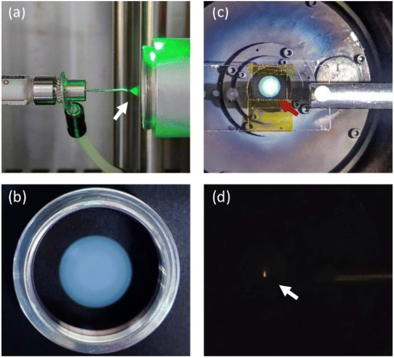 | ||
| Fig. 1 (a) Photograph showing the electrospray deposition of FNDs on an ITO-coated glass substrate mounted in a lens tube. The white arrow denotes the spray. (b) Photograph of a FND/ITO-coated glass substrate, prepared with a deposition time of 25 min. (c) Photograph of an FND/ITO-coated glass substrate in a synchrotron radiation beam path. The external white light was turned on to show the position of the substrate, which was mounted on a vacuum-compatible translation stage. (d) Photograph of an FND/ITO-coated glass substrate irradiated by a synchrotron radiation beam of 50 nm in wavelength. With a beam flux of 1.1 × 10¹² photons per s, the red fluorescence from NV0 centers hosted in FNDs could be readily seen with the naked eye in reflective mode when the external light was turned off. The red arrow in (c) denotes the FND film of ∼10 mm diameter, and the white arrow in (d) indicates the beam position, i.e., the red fluorescence spot with a size of about 3 × 3 mm2. | ||
An important consideration in preparing a uniform thin film of molecules or particles by electrospray deposition is that the substrate must be sufficiently electrically conductive to avoid charge accumulation that can lead to spray instability. This presents a major hurdle when applying it to non-conductive substrates like FOPs. To circumvent this problem, a thin layer of ITO was first coated on FOP by magnetron sputtering, followed by an oxygen plasma treatment to remove organic contaminants on the ITO surface before the FND coating by electrospray deposition. The method is straightforward, and the installation of FND-coated FOPs enables the manufacturing of low-cost, compact, broadband EUV/SXR-responsive CCD or CMOS image sensors with excellent photostability, high resolution, and exceptional contrast.
Results and discussion
FNDs
The FNDs used in this work were produced by bombarding synthetic type-Ib diamond powders with 10 MeV electrons, followed by vacuum annealing at 800 °C to create NV centers, as previously described.21,22 Two types of NV centers coexist in the FND matrix: NV0 and NV−.23 Their coexistence was revealed by optical excitation of the particles with a green laser, showing characteristic zero phonon lines at 576 nm and 638 nm for NV0 and NV−, respectively (Fig. S2†). Material characterization by scanning electron microscopy and dynamic light scattering revealed that the particles were monocrystalline, with a mean size of ∼100 nm in diameter and a zeta potential value of about −40 mV in distilled deionized water.20 The monocrystalline structure suggests their optical properties are similar to those of bulk diamonds, except for the fluorescence lifetimes of the electronically excited NV centers, which depend on the refractive indexes of their environments (Table S1†).24–28 An investigation of NV0 centers in FNDs drop-cast onto a glass coverslip revealed a lifetime of 28 ns.28An ideal inorganic scintillator should provide a combination of high light yield, short decay time, and good response linearity.29 To the best of our knowledge, diamonds with NV centers are the most promising carbon-based scintillators for meeting these requirements.20–22,30,31
FND-coated ITO/glass
Our previous studies have shown that the negatively charged FND particles could be well dispersed in a mixed water–methanol solution (30![[thin space (1/6-em)]](https://www.rsc.org/images/entities/char_2009.gif) :70, v/v) at a 10 mg mL−1 concentration.20 These particles formed a uniform thin film on an ITO-coated substrate by electrospray deposition in positive mode (See Fig. 1a and S3 in ESI† for the experimental setup). Fig. 1b shows a photograph of the FND film on an ITO-coated plate mounted in a Ø1′′ lens tube. The film is disk-like with a diameter of ∼12 mm and a transmission of 10–70% in the 400–800 nm wavelength region (Fig. S4†). It has a thickness of ∼1 μm, which is sufficient for the present application as the penetration depth of EUV/SXR light over 80–1400 eV in diamond is less than 1 μm (Fig. S1†).32 However, caution must be taken when using the scintillator, which lacks a protective layer in front of the FND film. This is because most chemicals strongly absorb light in the EUV/SXR regions; therefore, direct exposure of FNDs to these radiations is necessary for achieving the highest possible sensitivity. To ensure its practical use, we mounted the sensor in a filter holder for protection and installed it in a vacuum environment prior to operation.
:70, v/v) at a 10 mg mL−1 concentration.20 These particles formed a uniform thin film on an ITO-coated substrate by electrospray deposition in positive mode (See Fig. 1a and S3 in ESI† for the experimental setup). Fig. 1b shows a photograph of the FND film on an ITO-coated plate mounted in a Ø1′′ lens tube. The film is disk-like with a diameter of ∼12 mm and a transmission of 10–70% in the 400–800 nm wavelength region (Fig. S4†). It has a thickness of ∼1 μm, which is sufficient for the present application as the penetration depth of EUV/SXR light over 80–1400 eV in diamond is less than 1 μm (Fig. S1†).32 However, caution must be taken when using the scintillator, which lacks a protective layer in front of the FND film. This is because most chemicals strongly absorb light in the EUV/SXR regions; therefore, direct exposure of FNDs to these radiations is necessary for achieving the highest possible sensitivity. To ensure its practical use, we mounted the sensor in a filter holder for protection and installed it in a vacuum environment prior to operation.
A unique and novel application of the FND-coated ITO plate is to use it as an EUV/SXR viewing plate in reflective mode, similar to a laser viewing card. This distinctive utility is exemplified in Fig. 1c and d, where the FND film mounted on a translation stage was utilized to view the 50 nm radiation in a vacuum chamber at a synchrotron radiation facility in Taiwan.20 The orange emission, visible to the naked eye through the chamber's viewport, was a direct result of the film's exposure to EUV with a beam flux of 1.1 × 10¹² photons per s or a power of 4.4 μW. The emission band, peaking at ∼620 nm (Fig. S5†),20,22 was primarily derived from the NV0 centers implanted in the FND matrix. The use of this sensor plate dramatically simplifies the alignment procedures for the EUV/SXR beam, a critical step in mass spectrometric and photoelectron spectroscopic studies of clusters and nanoparticles in the gas phase using synchrotron radiations.33,34
The second application of the FND-coated ITO plate is to couple it with a lens system for EUV/SXR beam imaging. A diamond-based EUV imager (DEUVI) has been developed, with the plate operated in transmission mode, as shown in Fig. 2a.20 The optical system in this DEUVI system consisted of two Ø1′′ lenses (focal lengths of 25.4 mm and 35.1 mm) with an image magnification factor of 1.4 (Fig. 2b). A visible CMOS camera with a sensing area of 4.97 mm × 3.73 mm and a pixel size of 3.45 μm × 3.45 μm acquired the fluorescence images. To enable using DEUVI as a beam monitoring device, we sprayed FND particles on an ITO substrate supported by a polyethylene terephthalate (PET) film. The film has a thickness of ∼200 μm with a transmittance of ∼90% at 600 nm and has been widely used as a component in flexible optoelectronic applications. They can be conveniently cut into various sizes and shapes to fit specific needs using a continuous-wave CO2 laser. Fig. 2c shows a photograph of the FND-deposited ITO/PET film engraved with a laser-cut crosshair reticle from its backside. The reticle, with a fine line thickness of 0.5 mm, provides a distinctive measurement reference for visual inspections. It is a suitable replacement for the costly diamond screens prepared by chemical vapor deposition for X-ray beam monitoring.35 Employing this two-lens system, one can further carry out ON/OFF measurements to investigate the afterglow properties of the FND scintillator by replacing the CMOS camera with a photomultiplier tube. As shown in Fig. 2d, the fraction of the scintillation light that remained observable after switching off the synchrotron radiation was <0.01% at 50 nm. The value was over 2 orders of magnitude lower than that of Ce:YAG,36 which exhibited an afterglow lifetime of about 3 min.20
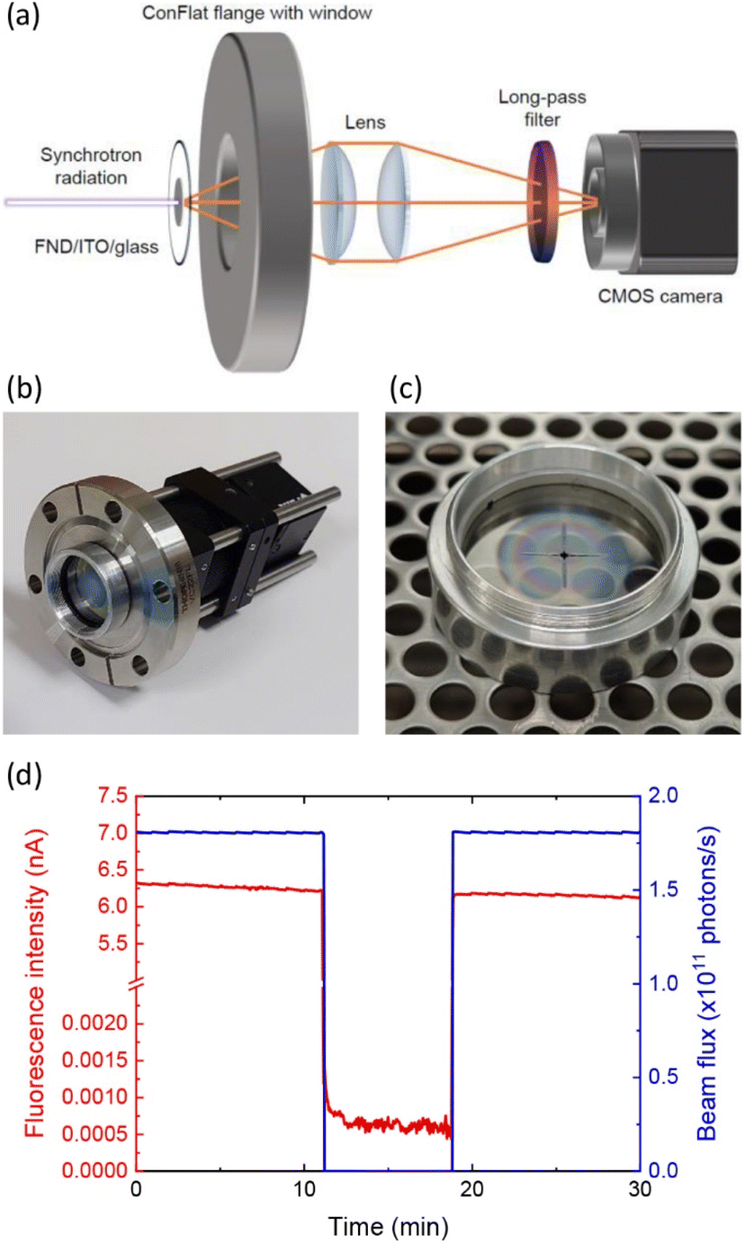 | ||
| Fig. 2 (a) Schematic diagram of the optical system used to image the EUV/SXR beam irradiated on an FND film deposited on an ITO-coated glass. (b) Photograph of a prototype of the diamond-based EUV imager (DEUVI). (c) Photograph of an FND thin film deposited on a PET film with a laser-cut crosshair reticle at the disk center. (d) Afterglow measurement for an FND thin film with 50 nm radiation. The light (with intensities in blue) was switched on and off to probe the temporal response of the scintillator. | ||
FND-coated ITO/FOP
Tested previously with 50 nm and 13.5 nm synchrotron radiations, the lens-coupled DEUVI system shown in Fig. 2a was found to provide a spatial resolution of 30 μm for the FND film of ∼1 μm thickness.20 Its noise-equivalent power density was 29 μW cm−2 Hz−1/2 at 13.5 nm. Although this noise level is sufficiently low to catch the images of the 13.5 nm radiation in an EUV scanner (such as that produced by ASML),37,38 it is desirable to enhance its sensitivity by collecting more fluorescence signals from the scintillators, thereby improving its usability and increasing its overall value. Replacing the two-lens system with an FOP attached to a CCD or CMOS image sensor offers a promising solution. To achieve this goal, the surface of an FOP of 3 mm thick was first made electrically conductive by coating with a thin layer (∼100 nm thick) of ITO using magnetron sputtering. The coating can be easily applied to FOPs, which are made of glass and consist of a bundle of micron-sized optical fibers. Electrospray deposition of FNDs on the ITO-coated FOPs was followed according to the abovementioned procedures. Fig. 3a shows a photograph of two FOPs with and without FND coating. A distinct concentric ring pattern of rainbow-like colors appeared on the FND-coated plate under white light, indicating the formation of a radially uniform scintillator layer.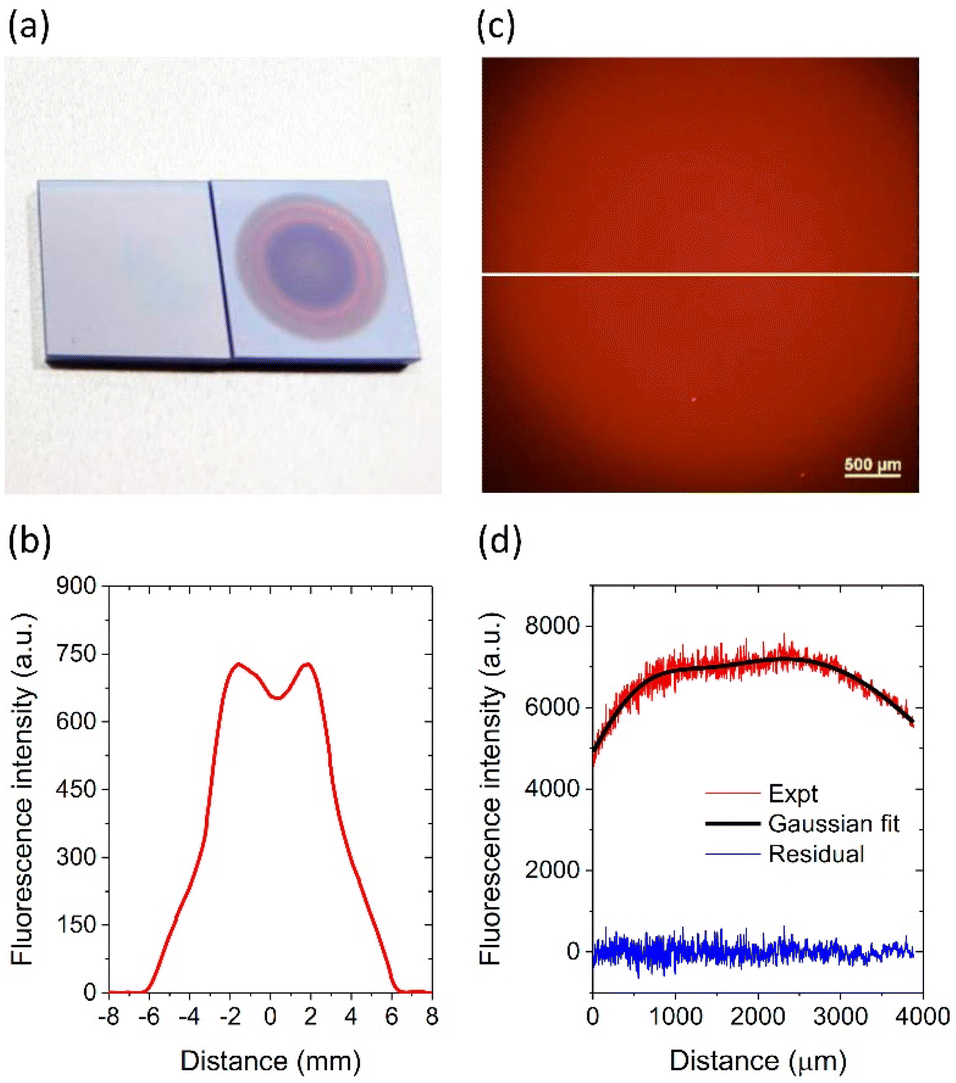 | ||
| Fig. 3 (a) Photograph of FOPs without (left) and with (right) FND coatings prepared by electrospray deposition. Dimensions of the FOPs were 14 × 14 mm2. (b) Fluorescence intensity line profile across the center of an FND film on an FOP. (c and d) Wide-field fluorescence image (c) and fluorescence intensity line profile (d) of an FND film on an FOP. The white line in (c) denotes the data points in (d), which were fitted with two Gaussian functions (black). | ||
To map out the thickness profile of the film, we performed fluorescence measurement through intra-defect excitation of the NV centers in FNDs using a green laser. As NV centers are perfectly photostable, the resulting fluorescence intensity can directly reflect the film thickness. Fig. 3b shows a typical fluorescence intensity profile of the FND film deposited on an ITO-coated FOP, measured by scanning the sample through a laser beam (0.7 mm diameter) in a home-built apparatus (Fig. S6†),39 as detailed in the Experimental section. The intensity profile is slightly asymmetrical with a full width at half maximum of 6.8 mm, which is larger than the image sensor's diagonal (6.2 mm) and well suited for use in this experiment. We further examined the film's uniformity by wide-field fluorescence imaging using a fluorescence microscope equipped with a 550 nm light source to excite the NV centers in FNDs and a 4× objective lens to collect the fluorescence. Fig. 3c and d show the image and a fluorescence intensity line profile across the FND film center over a 4 mm range. The line profile was convoluted with the film thickness and the excitation beam shape. By fitting the line profile with two Gaussian functions, we determined that the dispersion of the measured fluorescence intensities around the regression curve was 2.5%.
The FOP (3 mm thick) used in this work has a numerical aperture of 1 and a resolving power of 6 μm. Fibers in the plate are fused to form a vacuum-tight glass plate (Fig. 4a) and can be used as a zero-thickness window. Leveraging these properties, we attached the FND-coated FOP directly to the imaging sensor of a CMOS monochrome camera, rendering it EUV/SXR-responsive and vacuum-compatible. This was accomplished by gluing an FND-coated FOP plate on an aluminum holder to create an air-tight metal/glass seal and then mounting it on a high-vacuum 2.75′′ CF flange viewport through an O-ring (Fig. 4b). On the air side, the FOP was connected in direct contact with a board-level CMOS module (sensing area of 4.97 mm × 3.73 mm and a pixel size of 3.45 μm × 3.45 μm), forming a highly compact fiber-coupled DEUVI system (Fig. 4c). The design allowed the images produced on the FND film inside the vacuum chamber to be transported to the external surface of the FOP without losing light. The image distortion percentage is about 1%, according to the specifications.
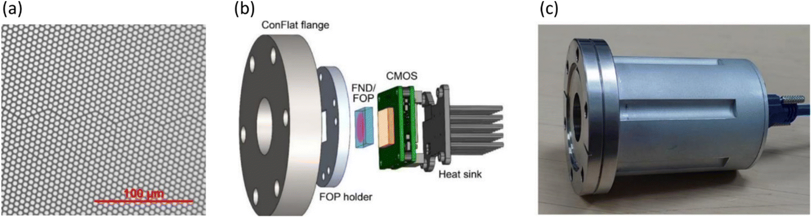 | ||
| Fig. 4 (a) Bright-field image of an FOP without FND coating. Individual fibers of 6 μm in diameter can be readily seen for the FOP. (b) Exploded view of a fiber-coupled DEUVI system. (c) A prototype of fiber-coupled DEUVI. | ||
Beam diagnostics
We first applied the FND/FOP-coupled CMOS camera as a beam diagnostic tool for EUV/SXR radiations from the BL08B beamline at the National Synchrotron Radiation Research Center (NSRRC), Taiwan.40 The beamline was equipped with two concave diffraction gratings, each having a ruling density of 350 and 1000 lines per mm, to disperse the EUV/SXR radiations over the wavelength range of 15.5–0.89 nm or the energy range of 80–1400 eV (Fig. S7 and S8†). Fig. 5 presents the images acquired under the same experimental conditions, with the grating (1000 lines per mm) scanned to select the radiation of interest (300–1400 eV). The beams were similar in size but differed significantly in shape. It was nearly vertically elliptical at 300 eV but became horizontally elliptical at 1400 eV. In contrast, the beam profile remained almost unchanged (e.g., inset in Fig. 6) after continuous beamline operation at fixed photon energies (such as 92 eV) for more than 6 h. The change in beam orientation by about 60° is most likely a result of the variation in beam divergence along the vertical and horizontal directions when the radiation is reflected from the grating and mirrors at different photon energies. We attribute the observations to the misalignment (including tilt, decentering, or a combination of both) of the incident beam relative to the diffraction grating. The ability to detect these minor beam alignment imperfections has direct and significant implications for the use of this device in EUV lithography for contemporary semiconductor chip manufacturing.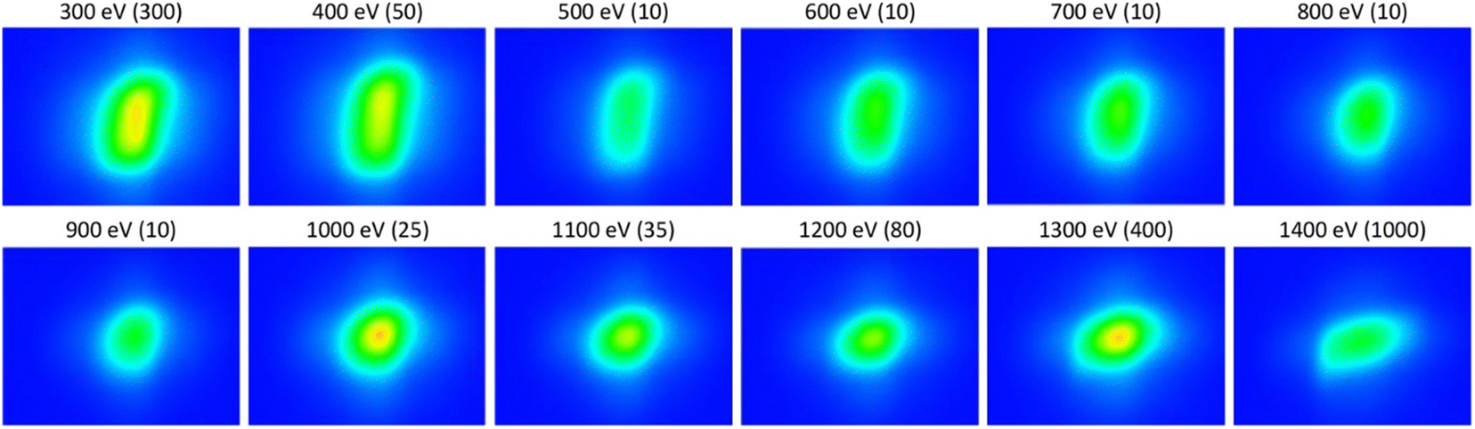 | ||
| Fig. 5 Variation of the beam shape with the photon energy of the synchrotron radiations over 300–1400 eV. Numbers in parentheses are exposure times in the units of ms. The sensing area of the CMOS camera was 4.97 mm × 3.73 mm. | ||
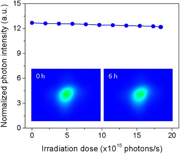 | ||
| Fig. 6 Photostability tests of an FND scintillator with 13.5 nm radiation from the BL08B beamline. The beam flux used was 7.7 × 10¹¹ photons per s with a beam spot area of ∼0.46 mm2. The measured fluorescence intensities were normalized by the photocurrents of a calibrated photodiode. (Inset) Images of the beam at the beginning (left) and end (right) of the measurements, showing a negligible change in beam profile after continuous operation for 6 h. | ||
In Fig. 6, we also show the result of a photostability test for the FND films using 13.5 nm radiation at an intensity of 24 μW mm−2 for more than 6 h. The fluorescence intensity decreased by approximately 4% after 6 h of continuous illumination of the FND film. The intensity decrease could be due to the gradual accumulation of charges in diamond lattice or surface defects,41 which may significantly reduce the photoluminescence quantum yield of implanted NV centers. Compared to commonly used organic phosphors such as sodium salicylate (SS), which degrade rapidly under continuous EUV excitation, FNDs significantly enhance scintillator durability and sensing performance. For instance, the photoluminescence intensity of FNDs changed by less than 2% after continuous irradiation with 60 nm light for 1 h, whereas the SS sensor experienced a decrease of approximately 42% during the same irradiation period.22
Finally, we compare the imaging capabilities of the fiber-coupled DEUVI system at 13.5 nm (92 eV) and 0.95 nm (1300 eV) with the radiations selected using different gratings. Fig. 7a and b show that both the beams were about 1 mm in diameter according to their line profiles across the beam centers (Fig. 7c and d). The response of the scintillator was highly linear, with the beam flux varying by more than 2 orders of magnitude (Fig. 8).22 Compared with the lens-coupled system, the fiber-coupled DEUVI was about 8-fold more sensitive (cf., Fig. S9† for representative images and intensity profiles). This sensitivity improvement agrees well with that reported by Uesugi et al.,42 who deposited Gd2O2S:Tb+ powders on a tapered FOP and a phosphor thickness of 20 mm. They found a 4× higher sensitivity in the fiber-coupled system than in a lens-coupled system when using their devices in X-ray computed tomography. For the EUV, by decreasing the beam flux to a level of 4 × 10⁸ photons per s (Fig. S10†), we determined a noise-equivalent power density of 0.25 μW cm−2 Hz−1/2 for the fiber-coupled DEUVI system at 13.5 nm. With such a high sensitivity, the device can be applied for beam diagnostics of not only EUV scanners in photolithography but also other EUV light sources such as gas discharge plasmas43 and high harmonic generation by table-top lasers.44
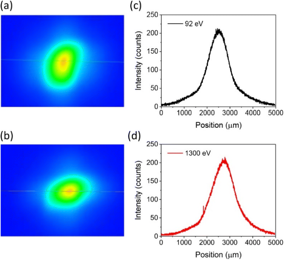 | ||
| Fig. 7 (a and b) Images and (c and d) intensity profiles of synchrotron radiations at 13.5 nm (a and c) and 0.95 nm (b and d), obtained with a fiber-coupled DEUVI system. The beam flux was 7.7 × 10¹¹ photons per s (and 4.5 × 10¹⁰ photons per s), and the exposure time used to acquire the image in (a) (and b) was 0.1 s (and 0.4 s) with a gain of 1 dB. The pixel size of the imaging sensor on the CMOS camera was 3.45 μm. | ||
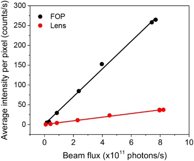 | ||
| Fig. 8 Dependence of average image intensities on the beam flux of 13.5 nm radiation using fiber-coupled DEUVI and lens-coupled DEUVI as the detectors. | ||
Conclusions
A new EUV/SXR-responsive image sensor with enhanced fluorescent coatings has been developed and characterized. The coating consists of 100 nm FNDs with a dense ensemble (∼10 ppm) of NV centers as built-in fluorophores.23 These nanomaterials are produced under extreme conditions by high-energy electron bombardment or ion irradiation,45,46 followed by vacuum annealing at 800 °C. As a result, they are radiation-hard and can survive EUV/SXR ablation processes over an extended period. Moreover, the NV centers are highly photostable and exhibit negligible afterglow, even in the SXR region. Using a positive electrospray deposition method, we have successfully fabricated highly uniform FND thin films (∼1 μm thickness) on ITO-coated glass, PET, and FOP surfaces. Tested with EUV/SXR radiation from a synchrotron facility, the FND thin films, formed on either ITO-coated glass substrates or ITO-coated PET plates, have been shown to be applicable as EUV/SXR viewing cards. Additionally, an 8-fold improvement in sensitivity is achieved by depositing FNDs directly on the FOP of a CMOS camera without deteriorating its imaging performance. The FND film is useful for imaging EUV/SXR radiations with a noise-equivalent power density of 0.25 μW cm−2 Hz−1/2, about 100× lower than the previously reported values at 13.5 nm using a lens-coupled system.20 The FND-based sensing and imaging devices offer low-cost, durable alternatives to existing EUV/SXR-responsive Si-based image sensors, which are prone to radiation damage from direct exposure to ionizing radiation above 10 eV. The production of larger, more uniform, and more robust FND thin films will be the focus of our future work.Experimental section
FND suspensions
NV centers in FNDs (∼100 nm diameter) were created by bombarding synthetic type-Ib diamond powders (Micron + MDA, Element Six) with high-energy particles, followed by vacuum annealing at 800 °C.45,46 The particles were first oxidized in air at 450 °C to remove graphitic carbon on their surface and then dispersed in 80:20 methanol/water solution at 4 mg mL−1 concentration as the stock solution. The particles in distilled deionized water were negatively charged with a zeta potential of −40 mV. Detailed characterizations of the sizes, surface properties, and fluorescence spectra of the 100 nm FNDs have been previously reported.20–22
FND films on ITO-coated glass plates
Fig. S3† shows a schematic diagram of the experimental setup for fabricating FND thin films on ITO-coated plates by electrospray deposition. Specifically, a 1 mL glass syringe (Gastight Syringe 1001RN, Hamilton) filled with a 4 mg mL−1 FND suspension in 80% methanol was first loaded on a syringe pump (LSP02-1B, KD Scientific). The syringe needle was 2 cm long and separated from the ITO substrate (Uni-onward, Taiwan) mounted on a digital rotator (MX-RD-Pro, DLAB) by about 10 mm. The ITO film was grounded with its holder, and a DC voltage of about +4 kV was applied to the needle from a high-voltage power supply (205A-05R, Bertan). The syringe pump ran continuously at a flow rate of 90 μL h−1 with the ITO-coated substrate rotating at 10 rpm during the sample preparation. A stable spray was established by fine adjustment of the DC voltage, confirmed by observing a steady stream of small droplets through light scattering from a green laser beam. The typical time of depositing an FND film of 1 μm thickness20 on an electrically conductive substrate was 25 min.FND films on ITO-coated FOPs
FOPs consisting of Schott 47A Glass with extra-mural absorption as the substrate (3 mm thickness) were obtained from commercial sources (Edmund Optics or Schott). These plates were first cut to a size of 14 × 14 mm2 to match the dimensions of the imaging sensor (IMX273, Sony) in a CMOS camera (BFS-U3-16S2M-BD, FLIR) and then coated with a thin layer (∼100 nm thick) of ITO by magnetron sputtering (UCSM Technology, Taiwan). The ITO-coated FOP was treated with oxygen plasma for 5 min before electrospray deposition. To ensure proper grounding of the ITO-coated FOP during electrospray deposition, the plate was additionally covered with a disk-shaped stainless steel foil (0.1 mm thick) having a 12 mm diameter hole at its center before the plasma and electrospray treatments.Coating thickness mapping
The variation of the FND film thickness across the ITO/glass substrate in the radial direction was measured using a green laser for the intra-defect excitation of NV centers in FNDs. Fig. S6† shows a home-built apparatus for such measurement.39 The apparatus consisted of a lock-in amplifier, which generated a sinewave, triggering a current amplifier to drive an electromagnetic coil. The sinewave frequency was 102.4 Hz, and the magnetic field strength was 30 mT (root-mean-square values). A continuous-wave 532 nm laser excited the FND film mounted on a motorized translation stage and situated above the electromagnetic coil. The magnetically modulated fluorescence was collected by an objective lens and detected by a photomultiplier tube. The lock-in amplifier analyzed the resulting electrical signals. Further information about the working principle of the magnetic modulation method and additional experimental details can be found in ref. 39.Optical microscopy
Bright-field and photoluminescence images of FND films were acquired using a fluorescence microscope system (Eclipse Ti2-E, Nikon) equipped with a UV-vis light source (D-LEDI, Nikon). Photoexcitation was carried out at 550 nm with a spot size of 4 mm in diameter, and the resulting fluorescence from NV centers in FNDs was collected through a 4× objective lens and detected over 600–800 nm by a CCD camera. The same microscope was applied to obtain the bright-field images of FOPs.Synchrotron radiation
Synchrotron radiation images were acquired in two separate end-stations connected to the beamlines BL03A and BL08B of Taiwan Light Source at NSRRC. The current of circulating electrons in the 1.5 GeV storage ring was 360 mA in top-up mode. Fig. S7† shows an optical layout of the BL08B beamline, which was equipped with a bending-magnet source.40 The beam, after being reflected through the grating, was focused by mirrors at a point approximately 50 cm before the sample position. At 400 eV, the focused beam size was measured to be about 0.55 mm vertical and 2.0 mm horizontal, when the widths of both entrance and exit slits were set at 50 μm.40 To further reduce the beam size, a screen plate with an aperture of 1 mm in diameter was placed about 20 cm before the focus. Photon fluxes of the beam after passing through the aperture were measured with a calibrated electron photodetector (AXUV100G, Opto Diode). Details of the design and characteristics of the BL03A beamline can be found elsewhere.20,22In the first experiment, the synchrotron radiation beam was shined on an FND/ITO film mounted on a lens tube attached to a 2.75′′ CF flange viewport with a Ø1′′ window (Fig. 2a). The fluorescence emission was collected with an imaging system composed of two Ø1′′ plano-convex lenses (LA1951-A and LA4052, Thorlabs) having focal lengths of 25.4 mm and 35.1 mm in series. The signals were finally detected by a CMOS camera (BFS-U3-16S2M-CS, FLIR) or a photomultiplier tube (PMT1001, Thorlabs). In the second experiment, the beam was shined on an FND film coated on an FOP, which was sealed on a 2.75′′ CF flange (Fig. 4b) mounted on a vacuum chamber of the BL08B beamline. On the air side, the imaging sensor (IMX273, Sony) of a CMOS monochrome camera (BFS-U3-16S2M-BD, FLIR) was physically attached to the FOP to acquire fluorescence images of the synchrotron radiation. Both the lens-coupled and fiber-coupled DEUVI systems were vacuum-compatible.
Data availability
The data supporting the findings of this study are available within the article, its ESI materials,† and upon request from the corresponding author.Author contributions
Yuen Yung Hui: conceptualization, methodology, formal analysis, investigation, writing – original draft, writing – review & editing. Chen-Yu Ho: methodology, investigation. Teng-I. Yang: conceptualization, methodology, formal analysis, investigation. Tzu-Ping Huang: methodology, investigation. Bing-Ming Cheng: conceptualization, writing – review & editing. Yin-Yu Lee: methodology, investigation, resources, writing – review & editing. Huan-Cheng Chang: conceptualization, methodology, formal analysis, writing – original draft, writing – review & editing, supervision, funding acquisition.Conflicts of interest
There are no conflicts to declare.Acknowledgements
This work was supported by Academia Sinica and the Ministry of Science and Technology, Taiwan, with Grant No. 113-2221-E-001-011-MY2. We thank NSRRC for providing the EUV/SXR beamlines and Alex Wang and Prof. Chia-Chun Wang for technical assistance in obtaining images in Fig. 1c and d.Notes and references
- D. Attwood, in Soft X-Rays and Extreme Ultraviolet Radiation: Principles and Applications, Cambridge University Press, Cambridge, 1999, ch. 1, p. 2 Search PubMed.
- B. Wu and A. Kumar, J. Vac. Sci. Technol., B:Microelectron. Nanometer Struct.–Process., Meas., Phenom., 2007, 25, 1743–1761 CrossRef CAS.
- EUV Lithography, ed. V. Bakshi, SPIE, Bellingham, 2nd edn, 2018 Search PubMed.
- A. Bharti, A. Turchet and B. Marmiroli, Front. Nanotechnol., 2022, 4, 835701 CrossRef.
- T. Higashiguchi, T. Otsuka, N. Yugami, W. Jiang, A. Endo, B. Li, D. Kilbane, P. Dunne and G. O'Sullivan, Appl. Phys. Lett., 2011, 99, 191502 CrossRef.
- L. K. Nanver, in Advances in Photodiodes, ed. G.-F. Dalla Betta, IntechOpen, London, 2011, ch. 10, pp. 205–224 Search PubMed.
- D. F. Edwards, in Handbook of Optical Constants of Solids, ed. E. D. Palik, Academic Press, Boston, 1985, vol. 1, pp. 547–569 Search PubMed.
- H. P. Garnir and P.-H. Lefèbvre, Nucl. Instrum. Methods Phys. Res., Sect. B, 2005, 235, 530–534 CrossRef CAS.
- T. Harada, N. Teranishi, T. Watanabe, Q. Zhou, J. Bogaerts and X. Wang, Appl. Phys. Express, 2019, 13, 016502 CrossRef.
- W. Zheng, L. Jia and F. Huang, iScience, 2020, 23, 101145 CrossRef CAS.
- A. Deslandes, A. B. Wedding, S. R. Clarke, J. G. Matisons and J. S. Quinton, in Smart Structures, Devices, and Systems II, ed. S. F. Al-Sarawi, SPIE, Bellingham, 2005, vol. 5649, pp. 616–626 Search PubMed.
- R. C. Catura, D. W. Duncan, L. Shing, T. D. Tarbell and C. J. Wolfson, in EUV, X-Ray, and Gamma-Ray Instrumentation for Astronomy IX, ed. O. H. W. Siegmund and M. A. Gummin, SPIE, Bellingham, 1998, vol. 3445, pp. 291–297 Search PubMed.
- W. A. R. Franks, M. J. Kiik and A. Nathan, IEEE Trans. Electron Devices, 2003, 50, 352–358 CrossRef CAS.
- Z. Yang, T. Wang, X. Xu, J. Yao, L. Xu, S. Wang, Y. Xu and J. Song, J. Phys. Chem. Lett., 2023, 14, 326–333 CrossRef CAS.
- L. Wang, K. Fu, R. Sun, H. Lian, X. Hu and Y. Zhang, Nano-Micro Lett., 2019, 11, 52 CrossRef.
- X. Zhang, Y. Shi, X. Wang, Y. Liu and Y. Zhang, ACS Nano, 2022, 16, 21576–21582 CrossRef CAS PubMed.
- S. Zhao, Z. Jia, Y. Huang, Q. Qian, Q. Lin and Z. Zang, Adv. Funct. Mater., 2023, 33, 2305858 CrossRef CAS.
- C. Huang, G. Xia, Y. Chang, J. Hong and H. Lu, OSA Continuum, 2019, 2, 1065–1079 CrossRef CAS.
- F. Bensebaa, in Interface Science and Technology, ed. F. Bensebaa, Elsevier, Amsterdam, 2013, vol. 19, ch. 4, pp. 185–277 Search PubMed.
- T.-I. Yang, Y. Y. Hui, J.-I. Lo, Y.-W. Huang, Y.-Y. Lee, B.-M. Cheng and H.-C. Chang, Nano Lett., 2023, 23, 9811–9816 CrossRef CAS.
- H.-C. Lu, Y.-C. Peng, S.-L. Chou, J.-I. Lo, B.-M. Cheng and H.-C. Chang, Angew. Chem., Int. Ed., 2017, 56, 14469–14473 CrossRef CAS PubMed.
- H.-C. Lu, J.-I. Lo, Y.-C. Peng, S.-L. Chou, B.-M. Cheng and H.-C. Chang, ACS Appl. Mater. Interfaces, 2020, 12, 3847–3853 CrossRef CAS.
- H.-C. Chang, W. W.-W. Hsiao and M.-C. Su, in Fluorescent Nanodiamonds, Wiley, Hoboken, 2019 Search PubMed.
- G. Liaugaudas, G. Davies, K. Suhling, R. U. A. Khan and D. J. F. Evans, J. Phys. Condens. Matter, 2012, 24, 435503 CrossRef CAS PubMed.
- D. Gatto Monticone, F. Quercioli, R. Mercatelli, S. Soria, S. Borini, T. Poli, M. Vannoni, E. Vittone and P. Olivero, Phys. Rev. B: Condens. Matter Mater. Phys., 2013, 88, 155201 CrossRef.
- E. Fraczek, V. G. Savitski, M. Dale, B. G. Breeze, P. Diggle, M. Markham, A. Bennett, H. Dhillon, M. E. Newton and A. J. Kemp, Opt. Mater. Express, 2017, 7, 2571–2585 CrossRef CAS.
- T.-I. Yang, T. Azuma, Y.-W. Huang, Y. Y. Hui, C.-T. Chiang and H.-C. Chang, J. Chin. Chem. Soc., 2023, 70, 451–459 CrossRef CAS.
- J. Storteboom, P. Dolan, S. Castelletto, X. Li and M. Gu, Opt. Express, 2015, 23, 11327–11333 CrossRef CAS.
- S. E. Derenzo, M. J. Weber, E. Bourret-Courchesne and M. K. Klintenberg, Nucl. Instrum. Methods Phys. Res., Sect. A, 2003, 505, 111–117 CrossRef CAS.
- S. Stoupin, S. Antipov and A. M. Zaitsev, J. Synchrotron Radiat., 2020, 27, 708–712 CrossRef CAS.
- A. Umemoto, T. Iida, M. Yoshino, A. Yoshikawa and S. Nomura, Nucl. Instrum. Methods Phys. Res., Sect. A, 2023, 1057, 168789 CrossRef CAS.
- S. Adachi, in Optical Constants of Crystalline and Amorphous Semiconductors: Numerical Data and Graphical Information, ed. S. Adachi, Springer US, Boston, MA, 1999, ch. A1, pp. 5–17 Search PubMed.
- C.-C. Su, Y. Yu, P.-C. Chang, Y.-W. Chen, I.-Y. Chen, Y.-Y. Lee and C. C. Wang, J. Phys. Chem. Lett., 2015, 6, 817–823 CrossRef CAS PubMed.
- M. Ahmed and O. Kostko, Phys. Chem. Chem. Phys., 2020, 22, 2713–2737 RSC.
- M. Degenhardt, G. Aprigliano, H. Schulte-Schrepping, U. Hahn, H.-J. Grabosch and E. Wörner, J. Phys.: Conf. Ser., 2013, 425, 192022 CrossRef.
- M. Benk and K. Bergmann, Rev. Sci. Instrum., 2009, 80, 033113 CrossRef.
- H. Meiling, H. Meijer, V. Banine, R. Moors, R. Groeneveld, H.-J. Voorma, U. Mickan, B. Wolschrijn, B. Mertens, G. van Baars, P. Kürz and N. Harned, in Emerging Lithographic Technologies X, ed. M. J.Lercel, SPIE, Bellingham, 2006, vol. 6151, pp. 49–60 Search PubMed.
- C.-P. Wang, B. J. Lin, P.-J. Wu, J.-R. Shih, Y.-D. Chih, J. Chang, C. J. Lin and Y.-C. King, Nanoscale Res. Lett., 2022, 17, 5 CrossRef CAS PubMed.
- Y. Y. Hui, O. J. Chen, H.-H. Lin, Y.-K. Su, K. Y. Chen, C.-Y. Wang, W. W.-W. Hsiao and H.-C. Chang, Anal. Chem., 2021, 93, 7140–7147 CrossRef CAS.
- J.-Y. Yuh, S.-W. Lin, L.-J. Huang, H.-S. Fung, L.-L. Lee, Y.-J. Chen, C.-P. Cheng, Y.-Y. Chin and H.-J. Lin, J. Synchrotron Radiat., 2015, 22, 1312–1318 CrossRef CAS PubMed.
- M. Schreck, P. Ščajev, M. Träger, M. Mayr, T. Grünwald, M. Fischer and S. Gsell, J. Appl. Phys., 2020, 127, 125102 CrossRef CAS.
- K. Uesugi, M. Hoshino and N. Yagi, J. Synchrotron Radiat., 2011, 18, 217–223 CrossRef CAS PubMed.
- V. Banine and R. Moors, J. Phys. D:Appl. Phys., 2004, 37, 3207 CrossRef CAS.
- E. Goulielmakis and T. Brabec, Nat. Photonics, 2022, 16, 411–421 CrossRef CAS.
- Y.-R. Chang, H.-Y. Lee, K. Chen, C.-C. Chang, D.-S. Tsai, C.-C. Fu, T.-S. Lim, Y.-K. Tzeng, C.-Y. Fang, C.-C. Han, H.-C. Chang and W. Fann, Nat. Nanotechnol., 2008, 3, 284–288 CrossRef CAS.
- J.-P. Boudou, P. A. Curmi, F. Jelezko, J. Wrachtrup, P. Aubert, M. Sennour, G. Balasubramanian, R. Reuter, A. Thorel and E. Gaffet, Nanotechnology, 2009, 20, 235602 CrossRef.
Footnote |
| † Electronic supplementary information (ESI) available. See DOI: https://doi.org/10.1039/d4ra08013k |
| This journal is © The Royal Society of Chemistry 2025 |