
 Open Access Article
 This Open Access Article is licensed under a Creative Commons Attribution-Non Commercial 3.0 Unported Licence
Magnetic exchange coupling and photodetection multifunction characteristics of an MnSe/LaMnO3 heterostructure†
Ye Zhao‡
a,
Xingguo Gao‡a,
Ruilong Yangab,
Ke Yanga,
Jiarui Doua,
Jinzhong Guoa,
Xiaoting Yanga,
Guowei Zhou *ab and
Xiaohong Xu*ab
*ab and
Xiaohong Xu*ab
aSchool of Chemistry and Materials Science of Shanxi Normal University & Key Laboratory of Magnetic Molecules and Magnetic Information Materials of Ministry of Education, Taiyuan 030006, China. E-mail: zhougw@sxnu.edu.cn; xuxh@sxnu.edu.cn
bResearch Institute of Materials Science of Shanxi Normal University & Collaborative Innovation Center for Advanced Permanent Magnetic Materials and Techonology, Taiyuan 030006, China
First published on 3rd January 2025
Abstract
Artificial heterostructures are often realized by stacking different materials to present new emerging properties that are not exhibited by their individual constituents. In this work, non-layered two-dimensional α-MnSe nanosheets were transferred onto LaMnO3 (LMO) films to obtain a multifunctional heterostructure. The high crystal quality of the MnSe/LMO heterostructure was revealed by X-ray diffraction, Raman spectroscopy, and scanning electron microscopy measurements. The enhancement of the saturated magnetization and coercive field and synchrotron X-ray measurements indicated the magnetic exchange coupling effect present in this MnSe/LMO heterostructure. The exchange bias field and coercive field reached 400 Oe and 1013 Oe under a positive 5k Oe field-cooling process. Thus, an outstanding photodetector with photoresponsivity of 4.1 × 10⁻⁴ A W−1 and photo detectivity of 2.6 × 10⁸ jones was obtained with a luminescence of 532 nm for this MnSe/LMO heterostructure. The multifunction characteristics of magnetic exchange coupling and photodetection in this heterostructure are very useful for next-generation devices.
Introduction
Artificial heterostructures, achieved via stacking of similar materials, often exhibit novel properties that are distinct from those of their individual components. Conventional heterostructures, composed of materials from the same crystal structural family, have traditionally been favored owing to their ability to maintain structural quality with minimized defects.1–3 However, recent endeavors are focused on creating heterostructures that combine diverse material families, including classic semiconductor compounds, transition metal oxides with perovskite structures, and more recently, two-dimensional (2D) atomic structures with layered or non-layered morphology.4–6 These efforts are driven by the potential of such heterostructures to enable multifunctional devices. For instance, their strongly correlated electron systems manifest various physical phenomena, like superconductivity, ferroelectricity, and ferromagnetism, owing to the interplay of multiple freedom of parameters, including spin, orbital, charge, and lattice, resulting in intricate phase diagrams.7–9 The responsiveness of these materials to parameter modifications makes them promising candidates for the next-generation electronic devices. However, many of these variables are inherent to the material properties established during growth and are challenging to control in practical applications. To introduce additional functionalities, post-growth modifications or interfacing the correlated oxides with other functional materials is usually employed. Nonetheless, most of these oxides lack sensitivity to light.10,11 On the other hand, 2D layered or non-layered materials, like graphene and transition metal dichalcogenides, exhibit exceptional electronic and optical properties and can be transferred from their original growth substrates onto alternative platforms owing to their weak van der Waals bonding.12,13 These characteristics make them particularly valuable for heterogeneous integration applications. Therefore, the investigation of transferring the 2D materials with outstanding photoelectric effect on transition metal oxides with excellent magnetoelectric properties is very valuable for the next-generation multifunctional devices.In Mn-based chalcogenides, rock salt (α-phase) manganese selenide (MnSe) is a typical material owing to its excellent photoelectric behaviour and abundant crystal structures.14 Duan et al. reported that thermodynamically stable α-MnSe is a wide-bandgap p-type semiconductor with antiferromagnetic properties, offering significant potential in the magneto-optical and magneto-optoelectronic device applications.15 Zhai et al. utilised the spatially confined chemical vapor deposition (CVD) technique to produce 2D α-MnSe with controlled thickness. Its optical and optoelectronic characteristics were investigated to address spin-ordering effects on the magnetic phase transition.16 To date, the outstanding p-type semiconductor characteristic of α-MnSe has been utilised in optoelectrical devices and the weak magnetic property also has been found in our recent experiments.17–21 Stoichiometric bulk LMO is known to be a layered-type (A-type) antiferromagnet, in which Mn3+ is a Jahn–Teller ion with a t2g3eg1 occupancy and the in-plane interaction between adjacent Mn ions is ferromagnetic (FM) while the out-of-plane one is antiferromagnetic (AFM). In contrast to bulk LMO, there have been several controversies about magnetic phases in thin films. While some studies describe the appearance of FM behavior in stoichiometric thin films, other reports have shown that AFM order stays in the films thinner than 5 unit cells, and the FM phase in films thicker. Meanwhile, almost all experiments have unveiled an insulating feature of LMO films in both FM and AFM phases. Therefore, the LMO material does not affect the photoelectronic property of the MnSe semiconductor.
In this work, the reported multifunctional heterostructure consists of a non-layered α-MnSe and a ferromagnetic insulator LaMnO3 (LMO). The high crystal quality of MnSe/LMO heterostructure was supported by X-ray diffraction (XRD), Raman spectroscopy, and scanning electron microscopy (SEM) measurements. The obvious enhancement of saturated magnetization and coercive field of MnSe/LMO heterostructure compared to that with single materials indicates that the magnetic exchange coupling effect is observed in the field-cooling loops. The exchange bias field and coercive field reached 400 Oe and 1013 Oe under a positive field-cooling process. The X-ray photoelectron spectroscopy (XPS) measurement and synchrotron X-ray technologies indicate the antiparallel spin arrangement of Mn ions, which further support the mechanism of magnetic coupling. The outstanding photodetector with photoresponsivity of 4.1 × 10⁻⁴ A W−1 and photo detectivity of 2.6 × 10⁸ jones was obtained in luminescence of 532 nm for this MnSe/LMO heterostructure. This work demonstrates a paradigm to create multifunctional heterostructures from materials with disparate properties.
Experimental section
Growth process of MnSe/LMO
The growth process of ultrathin MnSe nanosheets was conducted using a low-pressure chemical vapor deposition (CVD) technique in a two-temperature zone tube furnace inside a quartz tube (2-inch). Se (powder, 99.999%, Alfa) was placed at the upstream holding at 370 °C (first heating zone). MnCl2 (powder, 99.9%, Alfa) was positioned in the middle of the furnace holding at 610–660 °C. A mica substrate was placed downstream (about 4.5 cm away from MnCl2 powder) and faced down. The LaMnO3 (LMO) films with different thicknesses were grown on (001)-oriented SrTiO3 substrates using the pulsed-laser deposition (PLD) system in the oxygen environment with PO2 100 mTorr. During the growth, the substrates were held at 750 °C. The wavelength of the KrF excimer laser was 248 nm and the laser fluence was 1.2 J cm−2. MnSe nanosheets were transferred onto a polydimethylsiloxane (PDMS) sheet using a wedging transfer method, and then mechanically transferred on LMO films using a transfer platform.Characterisation of MnSe/LMO
MnSe/LMO heterostructures were characterized using a confocal Raman system with 532 nm laser (Horiba Scientific), X-ray diffraction (XRD, Rigaku), X-ray photoelectron spectroscopy (XPS, Thermo Scientific), and scanning electron microscopy combined with X-ray energy-dispersive spectroscopy (SEM, EDS, JEOL, JSM-IT800). Magnetic properties were measured with a vibrating sample magnetometer using a physical property measurement system (QD, PPMS-VSM), and hysteresis curves were obtained after subtracting the diamagnetic background. X-ray absorption spectroscopy (XAS) and X-ray magnetic circular dichroism (XMCD) measurements were performed at the beamline BL12B-a of the National Synchrotron Radiation Laboratory. The laser direct writing was used to construct the device of two-probe electrodes and Cr/Au (10/80 nm) was thermally deposited on the MnSe sample as electrodes. The electrical properties were measured on a four-probe station equipped with a Keithley 4200 semiconductor analyser system. The optoelectronic properties were measured under the 532 nm lasers.Results and discussion
The non-layered α-MnSe nanosheets were grown on f-mica substrates by low-pressure CVD using high-purity MnCl2 and Se as the precursors.22 The LaMnO3 films of different thicknesses were grown on (111)-oriented SrTiO3 substrates by PLD. Then, a mass of MnSe nanosheets was transferred onto the LMO films through a wedging transfer method.23 The surface morphology of the obtained MnSe/LMO heterostructures was analyzed from SEM images. The obvious triangular shape of the MnSe nanosheet is shown in Fig. 1a. Fig. 1a also displays the EDS elemental mapping images of triangular MnSe nanosheets, which prove the uniform distribution of Mn and Se elements. Moreover, Fig. S1† illustrates that La and Sr elements also exist in the measured range. Fig. S1d† provides a quantitative analysis of the EDS spectrum. The Mn elements are attributed to MnSe and LMO layers so the stoichiometric ratio of MnSe cannot be obtained from this measurement. Moreover, the structural, magnetic, and optoelectronic properties were further measured for this MnSe/LMO sample. Raman spectra can be used for a comprehensive understanding of the information on lattice vibration mode and phase structure. Fig. 1b shows the Raman spectra of a single LMO film and MnSe/LMO heterostructure via excitation by a 532 nm laser. In the investigated range from 150 to 900 cm−1, the peak for the MnSe nanosheet appears at 253 cm−1.24 For the LMO film, the Raman peaks are located at 492 and 657 cm−1.25 To further identify the crystal structure of MnSe/LMO heterostructure, XRD patterns were collected as shown in Fig. 1c. The main diffraction peaks at 46.9° can be indexed to the (002) plane of single LMO films on the STO substrate. However, the peak of the LMO film is very close to that of the STO substrate so the half-peak width is increased at the (002) plane. The XRD peak at 58.5° can also be observed in the pattern of the MnSe/LMO heterostructure, indicating that the non-layered MnSe nanosheet is stable on the LMO film.26 The XRD patterns indicate that the transferred MnSe nanosheet on LMO film is well along the (222) plane, and the absence of peaks corresponding to original precursors and impurity phases confirm the formation of the high-quality MnSe/LMO heterostructure. The other peaks are attributed to the (001)-oriented STO substrate.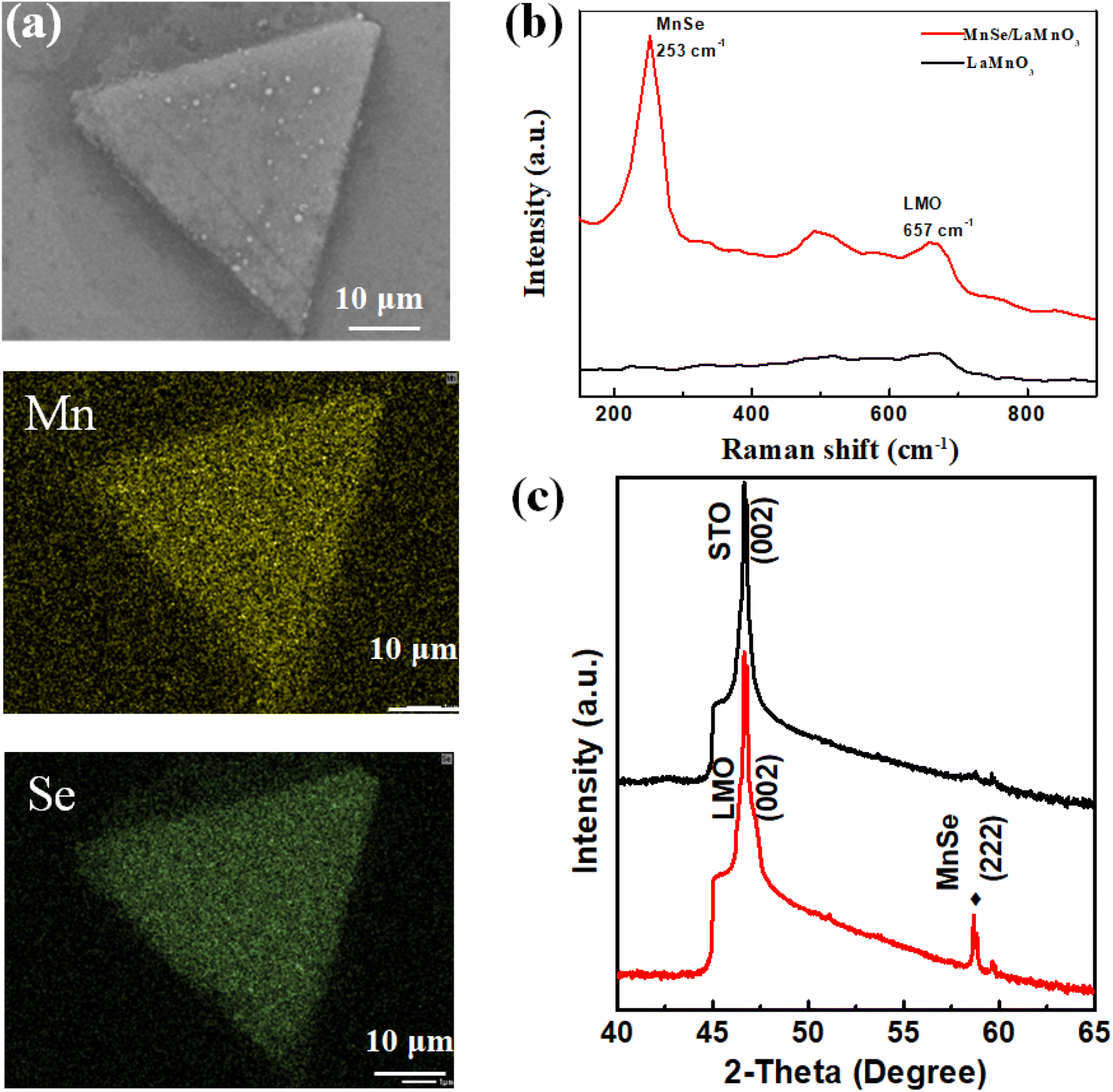 | ||
| Fig. 1 (a) SEM image of MnSe/LMO heterostructure. Mn and Se elemental images of MnSe/LMO heterostructure. (b) Raman spectra of MnSe/LMO heterostructure and the reference single LMO film. (c) XRD patterns of the obtained MnSe/LMO heterostructure and the reference single LMO film. The ♦ symbol is labeled as MnSe peak. | ||
In order to investigate the magnetic coupling effect in MnSe/LMO heterostructure, magnetic measurements were performed. As per previous results, the non-layered α-MnSe nanosheets present weak magnetic properties, and the LMO films show ferromagnetic properties.27 Fig. 2a shows the magnetic hysteresis loops of single MnSe nanosheets, 30 nm LMO film, and MnSe/LMO heterostructure at 10 K with the magnetic field along the in-plane direction. The saturated magnetization and coercive field in the MnSe/LMO heterostructure are larger than those in the other two single materials. This suggests the existence of the obvious magnetic coupling effect between the weaker magnetic MnSe and stronger magnetic LMO. In addition, the magnetic hysteresis loops of MnSe/LMO heterostructure were further measured after the sample was cooled from room temperature with in-plane magnetic fields of ±5k Oe. It is apparent that the horizontal loop shift direction is opposite to that of the cooling field for all samples, indicating the presence of the exchange bias effect (EBE) in this heterostructure. The exchange bias field (HEB) value is determined as HEB = |H+ + H−|/2, and the coercive field (HC) is evaluated as HC = |H+ − H−|/2, where H+ and H− represent the right and left side coercivity, respectively.28 As shown in Fig. 2b, the highlighted negative coercive field is −1413 Oe and the positive coercive field is 613 Oe. Therefore, the exchange bias field of 400 Oe and the coercive field of 1013 Oe are derived from the +5k Oe field-cooling loop. In contrast, on cooling in a −5k Oe field, a shift in the center of the magnetic loop along the magnetic field axis was observed towards positive fields. This behavior indicates that the exchange coupling effect is an intrinsic property in the MnSe/LMO heterostructure.7,28 The magnetic hysteresis loops of a single LMO film were cooled from room temperature with in-plane magnetic fields of ±5k Oe, as shown in Fig. S2.† The hysteresis loop shift is not observed in a single LMO film, indicating that the exchange coupling is induced by the MnSe/LMO heterostructure.
 | ||
| Fig. 2 (a) Magnetic hysteresis loops of LMO film, MnSe nanosheet, and MnSe/LMO heterostructure along the in-plane magnetic field at 10 K. (b) The positive field cooling (+5k Oe) and negative field cooling (−5k Oe) magnetic hysteresis loops of MnSe/LMO heterostructure at 10 K. | ||
To investigate the atomic composition and magnetic coupling effect within the MnSe/LMO heterostructure, X-ray photoelectron spectroscopy (XPS) measurements and synchrotron X-ray techniques were employed to analyze the core level states of Mn ions. Fig. 3a exhibits the Mn 2p spectra of MnSe/LMO heterostructure. The sample shows two main contributions of 641.5 and 654.0 eV, corresponding to Mn 2p3/2 and 2p1/2 positions, respectively. The other two peaks located at 646.2 and 658.0 eV may suggest the characteristics of Mn2+ and weak oxidation at the surface, respectively.29 In addition, the XPS spectra of La and Se ions are presented in Fig. S3.† To further support the magnetic exchange coupling effect in MnSe/LMO heterostructure, synchrotron X-ray curves of Mn elements were measured at 10 K. The polarized photon at 30° grazing incidence enters into the MnSe/LMO sample under the applied field of 5k Oe and the fluorescence yield mode.30 Fig. 3b shows the measured XAS/XMCD at Mn L edges, and the XMCD curve was calculated by the discrepancy of the XAS signal in the positive circle (PC+) and negative circle (NC−) along the applied field direction. The shoulder peak and main peak of the L3 edge are detected at 640.9 and 642.8 eV, respectively. These two different peaks are indicated as the Mn2+ ions in the MnSe layer and Mn3+ ions in the LMO layer. The corresponding XMCD signal at the L3 edge is antiparallel, suggesting the existence of a magnetic exchange coupling effect in the MnSe/LMO heterostructure.
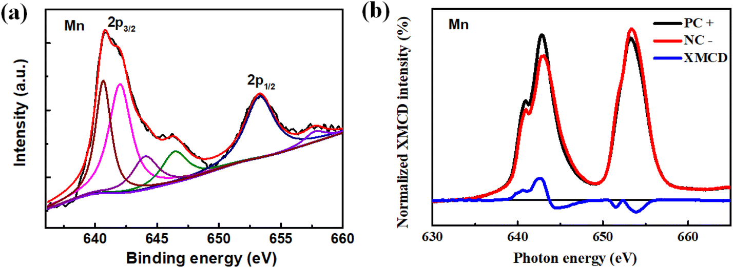 | ||
| Fig. 3 (a) XPS spectra of Mn 2p orbitals. (b) X-ray absorption spectroscopy and XMCD of Mn element for MnSe/LMO heterostructure at 10 K. | ||
Based on the previous discussion, excellent optoelectronic properties should exist in p-type semi-conductive MnSe nanosheets.31 To confirm whether this property exists in the MnSe/LMO heterostructure, the electronic and optoelectronic behaviors were studied herein. MnSe/LMO photodetectors were fabricated using a single-step laser direct writing technique to deposit Cr/Au as the electrode material. The photoresponse behaviours were thoroughly evaluated under ambient conditions, with a 532 nm laser as the excitation light source and the optical band-gap of α-MnSe is 2.0 eV. Fig. 4a illustrates the output curves measured with or without illumination. The source-drain current shows a linear correlation with the power density, confirming the ohmic contact between the MnSe/LMO channel and the electrodes. Fig. 4b exhibits the curves of photocurrent Iph dependence on voltage under different incident power densities. The photocurrent Iph, is defined by Iph = Ilight − Idark (Ilight is the irradiated current under illumination and Idark is the dark current).29–34 The photocurrent Iph increases linearly with increasing power densities, which indicates that the photocurrent is mainly determined by the absorbed photons. Moreover, the stability and reproducibility under periodical illumination with different incident wavelengths were measured to confirm the reversibility of the photoelectric conversion. Based on the same MnSe/LMO device sizes, the corresponding responsivity (Rλ) and detectivity (D*) under different incident lights were calculated; Fig. 4c shows the photon-to-electron conversion capability and the sensitivity of a photodetector with respect to dark current. Notably, Iph, Rλ, and D* are the main indicators for evaluating the photodetector performance. According to the formulas Rλ = Iph/PS and D* = RλS1/2/(2eIdark)1/2 (where Rλ, Iph, λ, P, S, and Idark are the responsivity, photogenerated current, incident wavelength, laser power density, effective detection area, and dark current, respectively), the MnSe device exhibits excellent photoresponse to 532 nm laser with a light intensity of 4.4 mW cm−2, an Iph of up to 5.2 × 10⁻⁶ μA, a maximum Rλ of up to 4.1 × 10⁻⁴ A W−1, and D* of up to 2.6 × 10⁸ jones. Fig. 4d displays the dependence of photocurrent on incident light of 532 nm intensity, in which the enhanced laser power density leads to monotonically increasing photocurrent. Therefore, the responsivity in MnSe/LMO devices is superior to those in the reported semiconductor materials such as α-MnSe, MoS2, and WS2.33–35
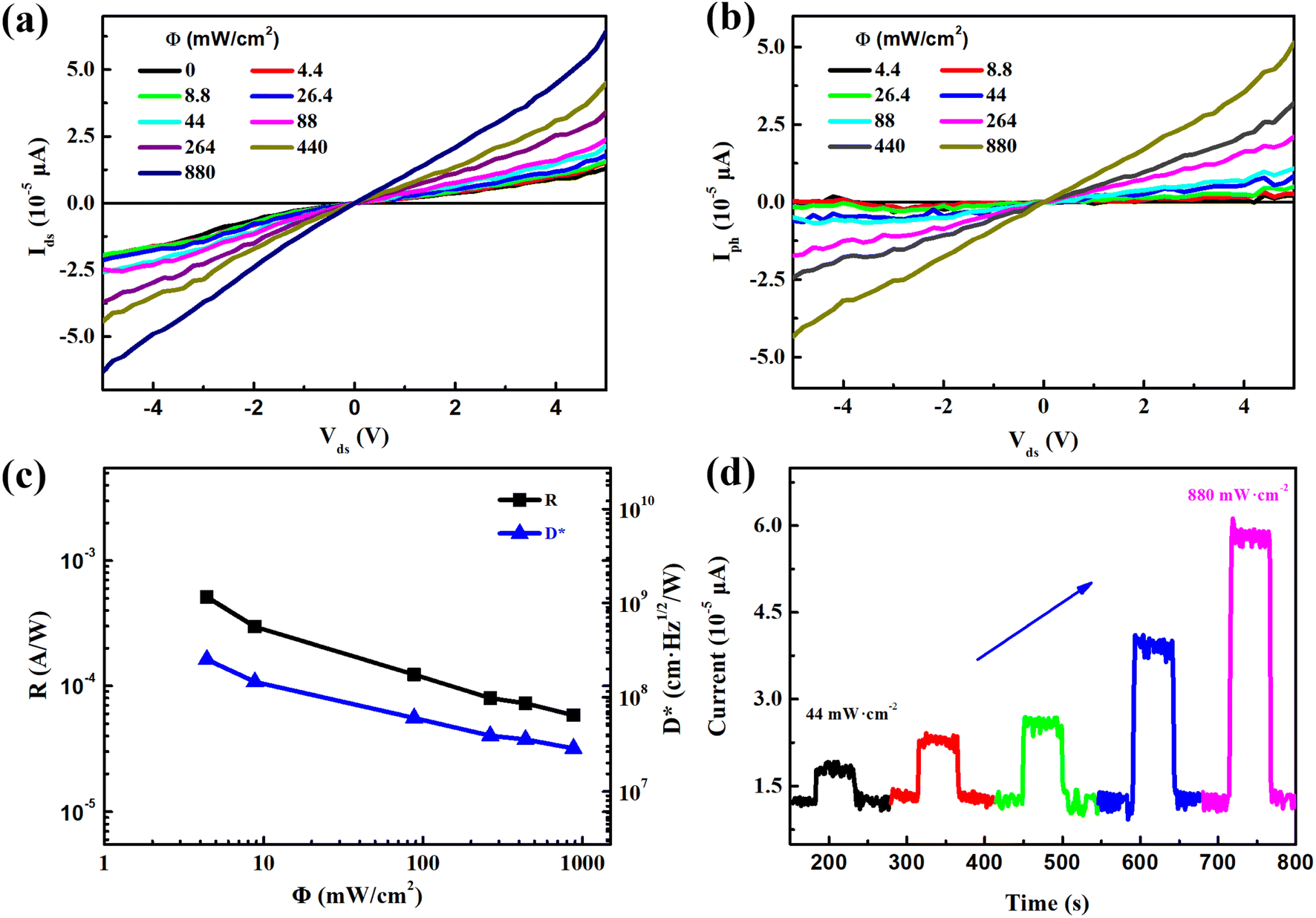 | ||
| Fig. 4 (a) Output characteristic curves of the MnSe/LMO photodetector under darkness and different illuminated power densities. (b) Photocurrent (Iph) as a function of incident power densities. (c) Responsivity and detectivity of the MnSe/LMO photodetector at various laser incident powers. (d) Photoresponse time dependence of light intensity curves of MnSe/LMO with various intensities at a bias voltage of 5 V. | ||
Conclusions
In this work, a ferromagnetic insulator LMO film with 30 nm thickness was deposited on (001)-oriented STO substrates. The non-layered α-MnSe nanosheets were transferred onto a PDMS sheet using a wedging transfer method, and then mechanically transferred on LMO films using a transfer platform. The high crystal quality of the MnSe/LMO heterostructure was supported by XRD, Raman spectroscopy, and SEM measurements. The obvious enhancement of saturated magnetization and coercive field and the synchrotron X-ray measurements indicate the magnetic exchange coupling effect in this MnSe/LMO heterostructure. The exchange bias field and coercive field reached 400 Oe and 1013 Oe, respectively, under a positive 5k Oe field-cooling process. Finally, the excellent photodetector with photoresponsivity of 4.1 × 10⁻⁴ A W−1 and photo detectivity of 2.6 × 10⁸ jones were obtained in the luminescence of 532 nm for this MnSe/LMO heterostructure. Therefore, the multifunction characteristics containing magnetic exchange coupling and photodetector in this heterostructure are very useful for next-generation devices.Data availability
Data underlying the results presented in this paper are not publicly available at this time but may be obtained from the authors upon reasonable request.Author contributions
Xu Xiaohong: funding acquisition, project administration, supervision, writing – review and editing. Zhao Ye: conceptualization, data curation, resources, writing – original draft. Yang Ruilong: conceptualization, data curation. Yang Ke: data curation. Dou Jiarui: investigation, methodology. Guo Jinzhong: investigation, methodology. Yang Xiaoting: data curation. Zhou Guowei: conceptualization, data curation, formal analysis, investigation, methodology, writing – review and editing.Conflicts of interest
The authors declare that they have no known competing financial interests or personal relationships that could have appeared to influence the work reported in this paper.Acknowledgements
This work is financially supported by the National Natural Science Foundation of China (No. 52471203, 12174237, 52002232, and 12304148) and the Fundamental Research Program of Shanxi Province (202303021221152). We acknowledge the XAS measurement at Beamline BL08U1A in Shanghai Synchrotron Radiation Facility (SSRF) and the XMCD measurement at Beamline BL12-a in the National Synchrotron Radiation Laboratory (NSRL).References
- H. Y. Hwang, Y. Iwasa, M. Kawasaki, B. Keimer, N. Nagaosa and Y. Tokura, Nat. Mater., 2012, 11, 103–113 CrossRef CAS PubMed.
- J. Chakhalian, J. W. Freeland, A. J. Millis, C. Panagopoulos and J. M. Rondinelli, Rev. Mod. Phys., 2014, 86, 1189 CrossRef CAS.
- J. Mannhart and D. G. Schlom, Science, 2010, 327, 5973 CrossRef PubMed.
- A. Ohtomo and H. Y. Hwang, Nature, 2004, 427, 423–426 CrossRef CAS PubMed.
- C. Song, B. Cui, F. Li, X. Zhou and F. Pan, Prog. Mater. Sci., 2017, 87, 33–82 CrossRef.
- C. Gong, L. Li, Z. Li, H. Ji, A. Stern, Y. Xia, T. Cao, W. Bao, C. Wang, Y. Wang, Z. Q. Qiu, R. J. Cava, S. G. Louie, J. Xia and X. Zhang, Nature, 2017, 546, 265–269 CrossRef CAS PubMed.
- G. Zhou, F. Jiang, J. Zang, Z. Quan and X. Xu, ACS Appl. Mater. Interfaces, 2018, 10, 1463–1467 CrossRef CAS PubMed.
- M. Alexe, M. Ziese, D. Hesse, P. Esquinazi, K. Yamauchi, T. Fukushima, S. Picozzi and U. Gösele, Adv. Mater., 2009, 21, 4452–4455 CrossRef CAS.
- H. Ji, Z. Yan, G. Zhou, X. Wang, J. Zhang, Z. Li, P. Kang and X. Xu, Appl. Phys. Lett., 2020, 117, 192402 CrossRef CAS.
- N. Reyren, S. Thie, A. D. Caviglia, L. Fitting Kourkoutis, G. Hammer, C. Richter, C. W. Schneider, T. Kopp, A.-S. Rüetschi, D. Jaccard, M. Gabay, D. A. Muller, J.-M. Triscone and J. Mannhart, Science, 2007, 317, 1196–1199 CrossRef CAS PubMed.
- H. Navarro, A. C. Basaran, F. Ajejas, L. Fratino, S. Bag, T. D. Wang, E. Qiu, V. Rouco, I. Tenreiro, F. Torres, A. Rivera-Calzada, J. Santamaria, M. Rozenberg and I. K. Schuller, Phys. Rev. Appl., 2023, 19, 040077 Search PubMed.
- H. Wang, Y. Wen, H. Zeng, Z. Xiong, Y. Tu, H. Zhu, R. Cheng, L. Yin, J. Jiang, B. Zhai, C. Liu, C. Shan and J. He, Adv. Mater., 2023, 2305044 Search PubMed.
- C. Dai, P. He, L. Luo, P. Zhan, B. Guan and J. Zheng, Sci. China Mater., 2023, 66, 859–876 CrossRef.
- M. J. Grzybowski, C. Autieri, J. Domagala, C. Krasucki, A. Kaleta, S. Kret, K. Gas, M. Sawicki, R. Bożek, J. Suffczyński and W. Pacuski, Nanoscale, 2024, 16, 6259–6267 RSC.
- Z. Zhang, B. Zhao, D. Shen, Q. Tao, B. Li, R. Wu, B. Li, X. Yang, J. Li, R. Song, H. Zhang, Z. Huang, Z. Zhang, J. Zhou, Y. Liu and X. Duan, Small Struct., 2021, 2, 2100028 CrossRef CAS.
- N. Zhou, Z. Zhang, F. Wang, J. Li, X. Xu, H. Li, S. Ding, J. Liu, X. Li, Y. Xie, R. Yang, Y. Ma and T. Zhai, Adv. Sci., 2022, 9, 2202177 CrossRef CAS PubMed.
- G. Zhou, H. Ji, Y. Bai, Z. Quan and X. Xu, Sci. China Mater., 2019, 1046–1152 CrossRef CAS.
- G. Zhou, H. Ji, W. Lin, J. Zhang, Y. Bai, J. Chen, M. Wu and X. Xu, Phys. Rev. B, 2020, 101, 024422 CrossRef CAS.
- Z. Chen, Z. Chen, Z. Q. Liu, M. E. Holtz, C. J. Li, X. Renshaw Wang, W. M. Lü, M. Motapothula, L. S. Fan, J. A. Turcaud, L. R. Dedon, C. Frederick, R. J. Xu, R. Gao, A. T. N'Diaye, E. Arenholz, J. A. Mundy, T. Venkatesan, D. A. Muller, L.-W. Wang, J. Liu and L. W. Martin, Phys. Rev. Lett., 2017, 119, 156801 CrossRef PubMed.
- M. Yang, K. Jin, H. Yao, Q. Zhang, Y. Ji, L. Gu, W. Ren, J. Zhao, J. Wang, E. Guo, C. Ge, C. Wang, X. Xu, Q. Wu and G. Yang, Adv. Sci., 2021, 2100177 CrossRef CAS PubMed.
- Y. J. Kim, C. Lee, H. Park, Y. Yeo, G. A. Safarina, D. D. Le, J. G. Kim, D. Bang, B. G. Cho, J. H. Park, K. T. Ko, T. Y. Koo, J. H. Shim and C. H. Yang, Nano Lett., 2022, 22, 1059–1066 CrossRef CAS PubMed.
- N. Li, L. Zhu, H. Shang, F. Wang, Y. Zhang, Y. Yao, J. Wang, X. Zhan, F. Wang, J. He and Z. Wang, Nanoscale, 2021, 13, 6953 RSC.
- G. F. Schneider, V. E. Calado, H. Zandbergen, L. Vandersypen and C. Dekker, Nano Lett., 2010, 10, 1912–1916 CrossRef CAS PubMed.
- M. Zhu, H. Xu, Z. Tan and L. Wang, Results Phys., 2023, 47, 106321 CrossRef.
- A. Kumar, M. Warshi, M. Gupta and P. R. Sagdeo, J. Magn. Magn. Mater., 2020, 514, 167210 CrossRef CAS.
- A. Panchwanee, V. Reddy, A. Gupta, R. J. Choudhary, D. M. Phase and V. Ganesan, Thin Solid Films, 2019, 669, 301–305 CrossRef CAS.
- C. Huang, C. Wang, C. Chang, Y. Lee, G. Huang, M. Wang and M. Wu, J. Magn. Magn. Mater., 2019, 483, 205–211 CrossRef CAS.
- G. Zhou, H. Ji, W. Lin, J. Zhang, Y. Bai, J. Chen, M. Wu and X. Xu, Phys. Rev. B, 2020, 101, 024422 CrossRef CAS.
- J. Zang, G. Zhou, Y. Bai, Z. Quan and X. Xu, Sci. Rep., 2017, 7, 10557 CrossRef PubMed.
- G. Zhou, C. Song, Y. Bai, Z. Quan, F. Jiang, W. Liu, Y. Xu, S. Dhesi and X. Xu, ACS Appl. Mater. Interfaces, 2017, 9, 3156–3160 CrossRef CAS PubMed.
- L. Hu, L. Cao, L. Li, J. Duan, X. Liao, F. Long, J. Zhou, Y. Xiao, Y. Zeng and S. Zhou, Mater. Horiz., 2021, 8, 1286–1296 RSC.
- C. Jin, X. Li, W. Han, Q. Liu, S. Hu, Y. Ji, Z. Xu, S. Hu, M. Ye, M. Gu, Y. Zhu and L. Chen, ACS Appl. Mater. Interfaces, 2021, 13, 34 CrossRef PubMed.
- D. O'Hara, T. Zhu, A. H. Trout, A. Ahmed, Y. Luo, C. Lee, M. Brenner, S. Rajan, J. Gupta, D. McComb and R. Kawakami, Nano Lett., 2018, 18, 3125–3131 CrossRef PubMed.
- Z. Yin, H. Li, H. Li, L. Jiang, Y. Shi, Y. Sun, G. Lu, Q. Zhang, X. Chen and H. Zhang, ACS Nano, 2012, 6, 74–80 CrossRef CAS PubMed.
- N. Perea-López, A. L. Elías, A. Berkdemir, A. Castro-Beltran, H. R. Gutiérrez, S. Feng, R. Lv, T. Hayashi, F. López-Urías, S. Ghosh, B. Muchharla, S. Talapatra, H. Terrones and M. Terrones, Adv. Funct. Mater., 2013, 23, 5511–5517 CrossRef.
Footnotes |
| † Electronic supplementary information (ESI) available: See DOI: https://doi.org/10.1039/d4ra06719c |
| ‡ These authors contributed equally to this paper. |
| This journal is © The Royal Society of Chemistry 2025 |