
 Open Access Article
 This Open Access Article is licensed under a Creative Commons Attribution-Non Commercial 3.0 Unported Licence
Improved self-powered perovskite CH3NH3PbI3/SnO2 heterojunction photodetectors achieved by interfacial engineering with a synergic effect
Guipeng Lia,
Huimin Zhanga,
Weihao Qinb and
Mingming Chen *a
*a
aDepartment of Microelectronics, Jiangsu University, Zhenjiang, Jiangsu 212013, China. E-mail: andychain@live.cn
bSchool of Materials Science and Engineering, East China University of Science and Technology, Shanghai, 200237, China
First published on 27th January 2025
Abstract
Lead halide perovskite heterojunctions have been considered as important building blocks for fabricating high-performance photodetectors (PDs). However, the interfacial defects induced non-radiative recombination and interfacial energy-level misalignment induced ineffective carrier transport severely limit the performance of photodetection of resulting devices. Herein, interfacial engineering with a spin-coating procedure has been studied to improve the photodetection performance of CH3NH3PbI3/SnO2 heterojunction PDs, which were fabricated by sputtering a SnO2 thin film on ITO glass followed by spin-coating a CH3NH3PbI3 thin film. It has shown that spin-coating of a SnO2 layer on the sputtered SnO2 thin films suppressed the surface oxygen vacancies of SnO2 thin films and up-shifted their conduction band, which suppressed the interfacial non-radiative recombination and enhanced the carriers transport at the CH3NH3PbI3/SnO2 interface, respectively. Accordingly, improved photodetection performance, such as the reduced dark current and increased photocurrent, has been observed in the CH3NH3PbI3/SnO2 heterojunction PDs, where the responsivity and detectivity of 0.077 A W−1 and 2.0 × 10¹¹ jones, respectively, at the zero bias have been demonstrated. These results show a simple way to suppress the interfacial non-radiative recombination and enhance the carrier transport at the interface to fabricate improved perovskite heterojunction PDs in the future.
Introduction
Photodetectors (PDs), which convert photons into electric charge, have attracted much attention recently owing to their important applications in various areas including digital imaging, optical communications, medical analysis, and environment monitoring.1–4 In general, PDs can be classified into two categories, i.e., photoconductors and photodiodes. The former ones possess a simple device structure but feature a high noise current and low photoconductive gains.5 In contrast, the latter ones have usually been characterized with a low noise current and high photon-to-electric conversion efficiencies owing to the presence of an interfacial barrier and a strong built-in electric field.6,7 Additionally, the photodiodes can operate without the requirement of a power supply. Heterojunctions, which are composed of two different semiconductors bound together, have been considered as important building blocks for photodiodes owing to simple fabrication process regarding free-of-controlled n- and p-type doping of selected semiconductors. In recent years, lead halide perovskites (LHPs) with a formula of ABX3 (where A is the CH3NH3+ (MA+), and HC(NH2)2+ (FA+); B is the Pb2−; X is the Cl−, Br−, and I−) have attracted much attention from the optoelectronics community due to their outstanding properties such as long charge carriers lifetime, long charge carriers diffusion length, high absorption coefficient, widely tunable energy bandgap, and low-temperature solution processability.8 Benefiting from these advantages, LHP heterojunctions have been considered as promising candidates for achieving efficient photodetection.9–12Generally, the working principles of PDs are similar to those of solar cells (SCs), where excess carriers are generated due to the valance-band-to-conduction-band transition upon light illumination, followed by the collection of excess carriers by the electrodes. As a wide bandgap semiconductor, tin dioxide (SnO2) features a high electron mobility, deep conduction band, and low-temperature processability, and has widely been employed as an electron transport layer to fabricate efficient SCs recently.13–15 Meanwhile, various PDs have recently been demonstrated based on LHP/SnO2 heterojunctions.16–18 Similar to LHP SCs, the performance of LHP PDs is mainly related to the collection efficiencies of excess carriers, which are limited by the trap-assisted non-radiative recombination and ineffective carrier transport.19 In heterojunction PDs, the former is mainly related to the bulk and interfacial defects, while the latter is owing to the energy-level misalignment at the heterojunction interface. Notably, various strategies have been explored to improve the crystalline quality of LHP thin films recently, which facilitated the rapid development of power conversion efficiency (PCE) of LHP SCs.20 Typically, doping of elements has resulted in an increase in grain sizes and a suppression of intrinsic defects (such as halide and Pb vacancies) in LHP thin films and nanocrystals.21 Besides, interfacial engineering with a thin dielectric layer and anchoring groups have been demonstrated but primarily to suppress the interfacial non-radiative recombination.22 In contrast, the alignment of energy-level at the heterojunction interface has seldom been explored before. Practically, both interfacial passivation and energy-level alignment are fundamental for fabricating high-performance heterojunction PDs.23 Herein, we showed the fabrication of improved solution-processed MAPbI3/SnO2 heterojunction PDs by employing a stacked SnO2 thin film prepared by sputtering and spin-coating methods in sequence. It showed that the subsequent spin-coating procedure behaved a synergic effect including a suppression of interfacial defects and alignment of the energy-level at the MAPbI3/SnO2 interface. Accordingly, a decreased dark current and an increased photocurrent have been demonstrated simultaneously in the MAPbI3/SnO2 heterojunction PDs. Finally, improved performance of photodetection with the responsivity and detectivity as high as 0.077 A W−1 and 2 × 10¹¹ jones, respectively, at the zero bias have been evidenced.
Experiments
MAPbI3/SnO2 heterojunctions (Fig. 1b) were fabricated by spin-coating a MAPbI3 thin film onto a stacked SnO2 thin film, which was prepared by sputtering a SnO2 thin film on cleaned ITO glasses then followed by spin-coating a thin SnO2 layer. In detail, the ITO glasses were cleaned with acetone, ethanol and DI water in sequence. After that, a thin SnO2 film was firstly grown using a sputtering method with a growth temperature of 500 °C and growth time of 10 min (labeled as SnO2-1). The RF power is 80 W. The Sn source was provided by a SnO2 target (99.99%). Ar/O2 with a flow of 55 sccm/5 sccm were used as working gas. Then, a thin SnO2 layer was grown by spin-coating to obtain the stacked SnO2 thin films (labeled as SnO2-2), in which the SnO2 precursor solution (3 wt%) was prepared by diluting SnO2 nanoparticles (∼20 nm) into DI water. Finally, MAPbI3 thin films were grown on SnO2-2 (labeled as MAPbI3-2) according to previous reports.24 The perovskite precursor was prepared by dissolving PbI2 and MAI into DMF/GBL/DMSO mixtures. The perovskite precursor was spin-coated with a two-step program (1000 rpm for 10 s and 5000 rpm for 20 s), where 400 μL toluene was dropped at 8 s of the second program. To reveal the roles of the spin-coated SnO2 thin layer, MAPbI3 thin films were directly prepared onto SnO2-1 (labeled as MAPbI3-1), as shown in Fig. 1a. The PDs were obtained by depositing a thin Au electrode with an area of 0.01 mm2 on the MAPbI3 thin films and an Ag paste on ITO.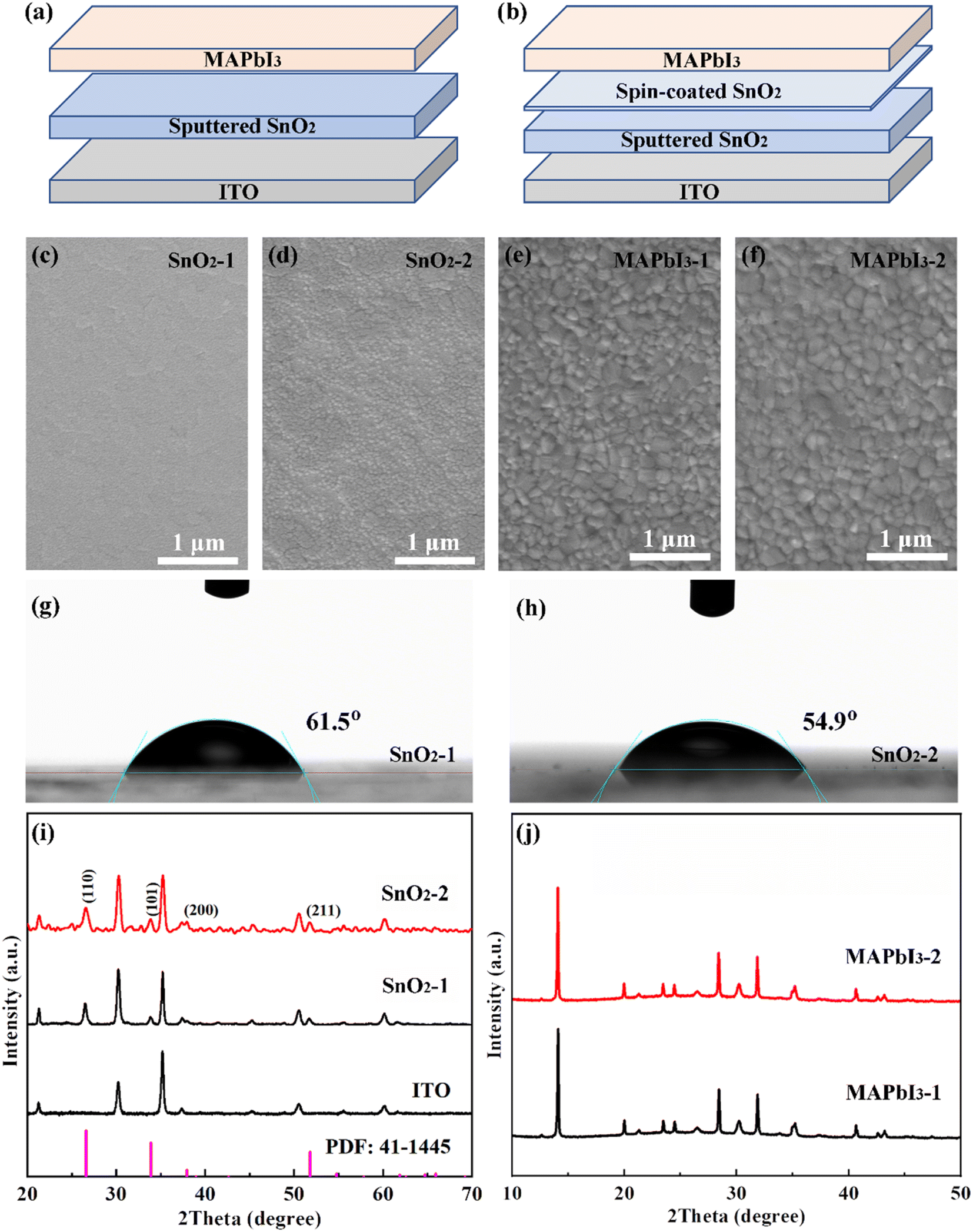 | ||
| Fig. 1 Characteristics of SnO2 and MAPbI3 thin films. (a and b) Scheme of MAPbI3/SnO2-1 and MAPbI3/SnO2-2 heterojunctions. (c–f) SEM images of SnO2 and MAPbI3 thin films. (g and h) Water contact angles of SnO2 thin films. (i and j) XRD patterns of SnO2 and MAPbI3 thin films. | ||
The morphology and structure of SnO2 and MAPbI3 thin films were studied by field-emission scanning electron microscopy (SEM, JSM-7800F) and X-ray diffraction (XRD, Bruker D8 with Cu Kα radiation of 1.54 Å). The steady-state photoluminescence (PL) spectra of MAPbI3 thin films were obtained with the excitation of a cw 405 nm laser. The power of the incident laser was modulated by an attenuator. The transient PL spectra were excited with a ps-pulse laser at 450 nm, and the data were recorded by a ps time-correlated single photon counting technique. The absorption spectra were collected on an ultraviolet-visible spectrophotometer. The atomic electron binding energies of SnO2 thin films were studied by X-ray photoelectron spectroscopy (XPS). The work function and energy band structure of SnO2 were studied by ultraviolet photoelectron spectroscopy technique (UPS) using He I as the excitation source.
The performance of MAPbI3/SnO2 heterojunction PDs was studied by a photoresponse system consisting of a Xe lamp, a monochromator, an electronic shutter, two probers, a microscope, a Keithley 2401 source-measure unit (SMU), and a semiconductor parameter analyzer (Keysight, B1500A). All experiments were carried out in the atmosphere with a humidity of ∼55–60%.
Results and discussions
Fig. 1c and d exhibit the SEM images of SnO2-1 and SnO2-2 thin films. It can be seen that the SnO2-1 thin films feature a smooth surface (Fig. 1c). This can be attributed to the high growth temperature (500 °C, as mentioned above), which facilitated the migration of species at the substrate surface. In comparison, a rough surface has been observed in the SnO2-2 thin films (Fig. 1d). According to previous report,25 a rough surface of buried layer increases the contact area at the MAPbI3/SnO2 interface, which improves the optical absorption in the MAPbI3 thin films. XRD were carried out to investigate the crystalline structures of SnO2-1 and SnO2-2 thin films, and the results are illustrated in Fig. 1i. As depicted, both the SnO2 thin films exhibit a similar crystalline structure. According to the XRD peaks which are located at 22.3°, 33.5°, 36.8°, and 52.5°, both the SnO2 thin films were crystallized into tetragonal with a space group of P42/mnm.Fig. 1e and f exhibit the SEM images of MAPbI3 thin films grown on SnO2-1 and SnO2-2. It shows that both the MAPbI3 thin films have a dense structure, which is fundamental for the subsequent fabrication of heterojunction PDs. Notably, the grain sizes of MAPbI3 thin films grown on SnO2-2 are around 200 nm, which is slightly larger than those grown on SnO2-1 (150 nm). In general, the MAPbI3 thin films with a larger grain size possess a decreased density of boundary defects, which is favorable to improve the photodetection performance of resulting PDs.26,27
Fig. 1j shows the XRD patterns of MAPbI3 thin films grown on SnO2-1 and SnO2-2. It shows that both the MAPbI3 thin films exhibit a similar crystalline structure and quality. Accordingly, the spin-coated SnO2 layer did not affect the growth of MAPbI3 thin films. Further observations show that the contact angle of SnO2-2 is comparable to that of SnO2-1 (Fig. 1g and h), which is responsible for the similar crystalline quality of the two MAPbI3 thin films.
As mentioned above, the SnO2-2 thin films were grown by sputtering and spin-coating SnO2 layers in sequence. In the latter case, the SnO2 precursor was prepared by diluting the SnO2 nanoparticles in DI water, therefore oxhydryl groups (OH−) tended to be doped into the SnO2 thin films.28 To verify this, XPS measurements were performed, and the results are shown in Fig. 2. As depicted in Fig. 2a, only Sn and O signals were observed in both the SnO2 thin films. This suggests that no impurities were incorporated during the preparation processes. Fig. 2b exhibits the O 1s core-level spectra of SnO2-1 and SnO2-2. The binding energies are observed at around 530.5 eV, 531.3 eV, and 532.5 eV, which are associated with Sn–O, oxygen vacancies (VO), and OH−, respectively.29 As reported, the content of various components can be qualitatively evaluated from their intensities of XPS peaks.29 Accordingly, the SnO2-2 shows an increased content of OH− and a reduced content of VO compared to SnO2-1. The former is related to the oxhydryl groups in the aqueous solution. The reasons for latter are unclear currently, but should be related to the SnO2 nanoparticles used. Importantly, it has reported that surface treatment with oxhydryl groups tuned the energy band of buried layers.30 As shown later, the SnO2-2 thin films show an increased conduction band, which aligned the energy-level at the MAPbI3/SnO2 interface. Meanwhile, the reduced VO suppressed the non-radiative recombination at the MAPbI3/SnO2 interface.31
 | ||
| Fig. 2 XPS curves of SnO2 thin films. (a) XPS survey spectra. (b) O 1s core-level spectra. | ||
Fig. 3 shows the steady-state and time-resolved PL spectra of MAPbI3 thin films grown on SnO2-1 and SnO2-2. It can be seen that the PL spectra captured from the front surface of MAPbI3 thin films exhibit similar intensity and lifetime (Fig. 3a and c), showing that both MAPbI3 thin films possess similar crystalline quality. This is in consistence with the XRD and SEM results shown above. Notably, the PL spectra captured from the back surface of MAPbI3 thin films exhibit distinct behaviors. As can be seen in Fig. 3b and d, the MAPbI3 thin films prepared on SnO2-2 exhibit a decreased PL intensity and lifetime. This suggests that the spin-coated SnO2 layer enhanced the extraction of electrons at the MAPbI3/SnO2 interface. Similar phenomena have been reported in graphdiyne decorated MAPbI3/SnO2 and Mg2+ decorated MAPbI3/NiO heterojunctions.32–34 As shown below, the slight up-shift of the conduction band of the SnO2-2 thin films aligned the interfacial energy-level, which is responsible for the decreased PL intensity and lifetime in the back surface of MAPbI3/SnO2-2 heterojunctions.
 | ||
| Fig. 3 Optical properties of MAPbI3 thin films prepared on SnO2-1 and SnO2-2. (a and b) Steady-state and (c and d) transient PL spectra. (e and f) Excitation power dependent PL spectra. The PL data in a and c were captured from the front surface of MAPbI3, as shown in Fig. 1c inset. The PL data in b, d, e and f were captured from the back surface of MAPbI3, as shown in Fig. 1d inset. | ||
Additionally, the interfacial defects at the MAPbI3/SnO2 interfaces were further studied from the excitation power dependent integrated PL, and the results are shown in Fig. 3e and f. As depicted in Fig. 3e, the PL spectra of both MAPbI3 thin films exhibit similar patterns with an increase in excitation power, showing that the recombination processes of excess carriers kept unchanged. Fig. 3f depicts the relationship between integrated PL intensity and corresponding excitation power. According to the trap-filling model, the PL intensity increases slowly with an increase in excitation power under the low excitation level, while it increases rapidly with the excitation power under the high excitation level.17,35,36 As a result, the density of trap states (ntrap) is proportional to the excitation power threshold of complete trap filling (Pth), i.e., ntrap ∝ Pth.17,35,36 As shown in Fig. 3f, the Pth for MAPbI3 grown on SnO2-1 and SnO2-2 were observed at 9.2 μW and 10.9 μW, respectively. This suggests that around 10% trap states have been reduced at the MAPbI3/SnO2-2 interface compared to MAPbI3/SnO2-1 interface. It is speculated that the reduced trap states at the MAPbI3/SnO2-2 interface is associated with the decreased surface VO of the SnO2-2 thin films as verified from XPS results shown above.
The energy band structure of SnO2 thin films was further studied by UPS and UV-vis absorption results. Fig. 4 exhibits the UPS spectra of SnO2-1 and SnO2-2 thin films. As reported before, the valence band maximum (EV) can be calculated from the following eqn (1):37
| EV = −[hν − (Ecutoff − EFV)] | (1) |
 | ||
| Fig. 4 (a and b) UPS and (c and d) absorption spectra of (a and c) SnO2-1 and (b and d) SnO2-2 thin films. The inset in (a and b) shows the energy band diagrams and in (c and d) shows the plot of (αhν)2 as a function of photon energy (hν). | ||
After depositing thin circular Au electrodes on MAPbI3 thin films and Ag paste on ITO, MAPbI3/SnO2 heterojunction PDs were fabricated. Fig. 5a illustrates the current–voltage (I–V) curves of MAPbI3/SnO2-1 and MAPbI3/SnO2-2 PDs captured in dark and under 540 nm illumination. As illustrated, the MAPbI3/SnO2-2 PDs shows a decreased dark current and an improved photocurrent compared to MAPbI3/SnO2-1 PDs. According to previous reports,17,40 the suppressed VO at the surface of SnO2-2 thin films is responsible for the reduced dark current and improved photocurrent. Besides, the up-shift of conduction band of SnO2-2 thin films further increases the photocurrent.41 Fig. 5b shows the current–time curves of both PDs captured at zero bias with 540 nm illumination switched on and off. As shown, the photocurrent of both PDs increases linearly with an increase in light power, in which the slope of 0.06 A W−1 and 0.02 A W−1 for MAPbI3/SnO2-2 and MAPbI3/SnO2-1 PDs were derived (Fig. 5b inset). Generally, the increased slope of light power dependent photocurrent in MAPbI3/SnO2-2 PDs suggests the improved photodetection performance of them.
 | ||
| Fig. 5 Photodetection performance of MAPbI3/SnO2 PDs. (a) I–V. (b) Current–time curves. (c) Responsivity. (d) Detectivity. The bias in (b–d) is 0 V. The light was illuminated at the back surface of MAPbI3 thin films. | ||
The photodetection performance of MAPbI3/SnO2 PDs was further evaluated from the responsivity and detectivity parameters. According to previous reports, the responsivity (R) and detectivity (D*) were calculated using the following eqn (2) and (3):17
 | (2) |
 | (3) |
Finally, the mechanisms of improved photodetection performance in MAPbI3/SnO2-2 PDs are discussed. Fig. 6 illustrates the photodetection processes of MAPbI3/SnO2-1 and MAPbI3/SnO2-2 PDs. Initially, electron–hole pairs were generated within the MAPbI3 thin films upon illumination. Then, the electrons were extracted by the SnO2 thin films owing to the interfacial electrical field and the holes moved toward the Au electrode. As a result, remarkable photocurrent has been observed in the MAPbI3/SnO2-1 and MAPbI3/SnO2-2 PDs. However, remarkable non-radiative recombination occurred at the MAPbI3/SnO2-1 interface (Fig. 6a) due to the high density of VO at the surface of SnO2-1 thin films. This resulted in an increased dark current and decreased photocurrent. In comparison, the non-radiative recombination was suppressed at the MAPbI3/SnO2-2 interface (Fig. 6b) owing to the suppressed VO at the surface of SnO2-2. Accordingly, improved photocurrent and decreased dark current have been observed simultaneously in the MAPbI3/SnO2-2 PDs. Besides, the up-shift of conduction band of SnO2-2 facilitated the electron transport at the MAPbI3/SnO2 interface (Fig. 6b), which further improved the photocurrent. Collectively, the spin-coating procedure behaved a synergic effect including reduced surface VO and increased conduction band of the SnO2, which accounted for the improved performance of photodetection of MAPbI3/SnO2-2 PDs.
 | ||
| Fig. 6 Photodetection processes of (a) MAPbI3/SnO2-1 and (b) MAPbI3/SnO2-2 PDs. | ||
In summary, performance-improved solution-processed MAPbI3/SnO2 heterojunction PDs have been fabricated by employing a stacked SnO2 thin film prepared by sputtering and spin-coating methods in sequence. It has shown that the spin-coating procedure have little impacts on the growth of MAPbI3 thin films, while it behaved a synergic effect such as reduced the surface VO and up-shifted the conduction band of SnO2 thin films. The former suppressed the interfacial non-radiative recombination, while the latter aligned the energy-level at the MAPbI3/SnO2 interface and further improved the carrier transport. On these basis, the MAPbI3/SnO2 heterojunction PDs with a stacked SnO2 thin film exhibited an improved photodetection performance in terms of reduced dark current and increased photocurrent, where an improved responsivity and detectivity of 0.077 A W−1 and 2.0 × 10¹¹ jones, respectively, at the zero bias have been achieved. The results provided in this work provide a simple strategy for suppressing the interfacial defects and aligning the energy-level simultaneously for improving the performance of perovskite heterojunction PDs in the future.
Data availability
The data that support the findings of this study are available from the corresponding authors upon reasonable request.Conflicts of interest
The authors have declared that no conflict of interest exists.References
- L. Li, H. Chen, Z. Fang, X. Meng, C. Zuo, M. Lv, Y. Tian, Y. Fang, Z. Xiao, C. Shan, Z. Xiao, Z. Jin, G. Shen, L. Shen and L. Ding, An Electrically Modulated Single-Color/Dual-Color Imaging Photodetector, Adv. Mater., 2020, 32(24), 1907257 CrossRef CAS PubMed.
- W. Wu, X. Wang, X. Han, Z. Yang, G. Gao, Y. Zhang, J. Hu, Y. Tan, A. Pan and C. Pan, Flexible Photodetector Arrays Based on Patterned CH3NH3 PbI(3-x)Cl(x) Perovskite Film for Real-Time Photosensing and Imaging, Adv. Mater., 2019, 31(3), 1805913 CrossRef PubMed.
- P. Büchele, M. Richter, S. F. Tedde, G. J. Matt, G. N. Ankah, R. Fischer, M. Biele, W. Metzger, S. Lilliu, O. Bikondoa, J. E. Macdonald, C. J. Brabec, T. Kraus, U. Lemmer and O. Schmidt, X-ray imaging with scintillator-sensitized hybrid organic photodetectors, Nat. Photonics, 2015, 9(12), 843–848 CrossRef.
- C. Bao, J. Yang, S. Bai, W. Xu, Z. Yan, Q. Xu, J. Liu, W. Zhang and F. Gao, High Performance and Stable All-Inorganic Metal Halide Perovskite-Based Photodetectors for Optical Communication Applications, Adv. Mater., 2018, 30(38), 1803422 CrossRef PubMed.
- J. Liu, M. Gao, J. Kim, Z. Zhou, D. S. Chung, H. Yin and L. Ye, Challenges and recent advances in photodiodes-based organic photodetectors, Mater. Today, 2021, 51, 475–503 CrossRef CAS.
- Y. Yan, Q. Wu, Y. Zhao, S. Chen, S. Hu, J. Zhu, J. Huang and Z. Liang, Air-Stable and Self-Driven Perovskite Photodiodes with High On/Off Ratio and Swift Photoresponse, Small, 2018, 14(41), 1802764 CrossRef PubMed.
- M. V. Kovalenko, L. Protesescu and M. I. Bodnarchuk, Properties and potential optoelectronic applications of lead halide perovskite nanocrystals, Science, 2017, 358(6364), 745–750 CrossRef CAS PubMed.
- L. K. Ono, Y. Qi and S. Liu, Progress toward Stable Lead Halide Perovskite Solar Cells, Joule, 2018, 2(10), 1961–1990 CrossRef CAS.
- D. Nodari, L. J. F. Hart, O. J. Sandberg, F. Furlan, E. Angela, J. Panidi, Z. Qiao, M. A. McLachlan, P. R. F. Barnes, J. R. Durrant, A. Ardalan and N. Gasparini, Dark Current in Broadband Perovskite-Organic Heterojunction Photodetectors Controlled by Interfacial Energy Band Offset, Adv. Mater., 2024, 36(33), 2401206 CrossRef CAS PubMed.
- Y. Zhang, C. Li, E. Bi, T. Wang, P. Zhang, X. Yang and H. Chen, Efficient Inverted Perovskite Solar Cells with a Low-Dimensional Halide/Perovskite Heterostructure, Adv. Energy Mater., 2022, 12(48), 2202191 CrossRef CAS.
- J. Zhuang, J. Wang and F. Yan, Review on Chemical Stability of Lead Halide Perovskite Solar Cells, Nano-Micro Lett., 2023, 15(1), 84 CrossRef CAS PubMed.
- J. Zhou and J. Huang, Photodetectors Based on Organic-Inorganic Hybrid Lead Halide Perovskites, Adv. Sci., 2018, 5(1), 1700256 CrossRef PubMed.
- L. Xiong, Y. Guo, J. Wen, H. Liu, G. Yang, P. Qin and G. Fang, Review on the Application of SnO2 in Perovskite Solar Cells, Adv. Funct. Mater., 2018, 28(35), 1802757 CrossRef.
- Q. Jiang, X. Zhang and J. You, SnO2 : A Wonderful Electron Transport Layer for Perovskite Solar Cells, Small, 2018, 1801154 CrossRef PubMed.
- C. Wu, B. Du, W. Luo, Y. Liu, T. Li, D. Wang, X. Guo, H. Ting, Z. Fang, S. Wang, Z. Chen, Y. Chen and L. Xiao, Highly Efficient and Stable Self-Powered Ultraviolet and Deep-Blue Photodetector Based on Cs2AgBiBr6/SnO2 Heterojunction, Adv. Opt. Mater., 2018, 6(22), 1800811 CrossRef.
- M. J. Paik, Y. Y. Kim, J. Kim, J. Park and S. I. Seok, Ultrafine SnO2 colloids with enhanced interface quality for high-efficiency perovskite solar cells, Joule, 2024, 8(7), 2073–2086 CrossRef CAS.
- P. Cheng, T. Zhao, M. Chen, S. Chen, X. Shen, Y. Liu, S. Yang, Z. Chen, X. Dong, Q. Wang and D. Cao, Improved Perovskite CH3NH3PbI3 Thin Films by ZIF-67 Additive Assisted Co Ion Doping toward High-Performance and Stable Photodetectors, Adv. Opt. Mater., 2023, 11(21), 2300757 CrossRef CAS.
- Y. Lin, Y. Bai, Y. Fang, Z. Chen, S. Yang, X. Zheng, S. Tang, Y. Liu, J. Zhao and J. Huang, Enhanced Thermal Stability in Perovskite Solar Cells by Assembling 2D/3D Stacking Structures, J. Phys. Chem. Lett., 2018, 9(3), 654–658 CrossRef CAS PubMed.
- Z. Yang, Y. Deng, X. Zhang, S. Wang, H. Chen, S. Yang, J. Khurgin, N. X. Fang, X. Zhang and R. Ma, High-Performance Single-Crystalline Perovskite Thin-Film Photodetector, Adv. Mater., 2018, 30(8), 1704333 CrossRef PubMed.
- D. Yang, R. Yang, K. Wang, C. Wu, X. Zhu, J. Feng, X. Ren, G. Fang, S. Priya and S. F. Liu, High efficiency planar-type perovskite solar cells with negligible hysteresis using EDTA-complexed SnO2, Nat. Commun., 2018, 9(1), 3239 Search PubMed.
- T. Bu, J. Li, F. Zheng, W. Chen, X. Wen, Z. Ku, Y. Peng, J. Zhong, Y. B. Cheng and F. Huang, Universal passivation strategy to slot-die printed SnO2 for hysteresis-free efficient flexible perovskite solar module, Nat. Commun., 2018, 9(1), 4609 CrossRef PubMed.
- W. Jang, Z. U. Rehman, M. Haris, J. S. Cho, J. Lim, M. S. Kim, J.-C. Lee, H. K. Lee and D. H. Wang, Oxide vacancy passivation through interface engineering of Tetraphenylethylene-Based Small-Molecule with sulfonate functional group for efficient organic photodetector, Chem. Eng. J., 2023, 472, 144847 CrossRef CAS.
- M. Sun, H. Zhang, C. Liang, C. Ji, X. Jing, F. Sun, Q. Song, F. You and Z. He, Exploring Electron Transporting Layer in Combination with a Polyelectrolyte for n–i–p Perovskite Solar Cells, Adv. Mater. Interfaces, 2020, 7(17), 2000412 CrossRef CAS.
- M. Abuhelaiqa, N. Shibayama, X.-X. Gao, H. Kanda and M. K. Nazeeruddin, SnO2/TiO2 Electron Transporting Bilayers: A Route to Light Stable Perovskite Solar Cells, ACS Appl. Energy Mater., 2021, 4(4), 3424–3430 CrossRef CAS.
- Y. Zheng, J. Kong, D. Huang, W. Shi, L. McMillon-Brown, H. E. Katz, J. Yu and A. D. Taylor, Spray coating of the PCBM electron transport layer significantly improves the efficiency of p-i-n planar perovskite solar cells, Nanoscale, 2018, 10(24), 11342–11348 RSC.
- W. Xu, G. Lei, C. Tao, J. Zhang, X. Liu, X. Xu, W. Y. Lai, F. Gao and W. Huang, Precisely Controlling the Grain Sizes with an Ammonium Hypophosphite Additive for High-Performance Perovskite Solar Cells, Adv. Funct. Mater., 2018, 28(33), 1802320 Search PubMed.
- B. Li, C. Liu and X. Zhang, SnO2-Based Interfacial Engineering towards Improved Perovskite Solar Cells, Nanomaterials, 2024, 14(17), 14171406 Search PubMed.
- J. Jia, C. Qian, Y. Dong, Y. F. Li, H. Wang, M. Ghoussoub, K. T. Butler, A. Walsh and G. A. Ozin, Heterogeneous catalytic hydrogenation of CO2 by metal oxides: defect engineering – perfecting imperfection, Chem. Soc. Rev., 2017, 46(15), 4631–4644 RSC.
- J. Liu, S. Li, S. Liu, Y. Chu, T. Ye, C. Qiu, Z. Qiu, X. Wang, Y. Wang, Y. Su, Y. Hu, Y. Rong, A. Mei and H. Han, Oxygen Vacancy Management for High-Temperature Mesoporous SnO2 Electron Transport Layers in Printable Perovskite Solar Cells, Angew. Chem., Int. Ed., 2022, 61(26), 202202012 Search PubMed.
- X. Wang, Y. Zhang, C. Zhou, D. Huo, R. Zhang and L. Wang, Hydroxyl-regulated BiOI nanosheets with a highly positive valence band maximum for improved visible-light photocatalytic performance, Appl. Catal., B, 2020, 268, 118390 CrossRef CAS.
- J. H. Lee, D. Shin, R. Rhee, S. Yun, K. M. Yeom, D. H. Chun, S. Lee, D. Kim, Y. Yi, J. H. Noh and J. H. Park, Band Alignment Engineering between Planar SnO2 and Halide Perovskites via Two-Step Annealing, J. Phys. Chem. Lett., 2019, 10(21), 6545–6550 CrossRef CAS PubMed.
- H. Min, D. Y. Lee, J. Kim, G. Kim, K. S. Lee, J. Kim, M. J. Paik, Y. K. Kim, K. S. Kim, M. G. Kim, T. J. Shin and S. Il Seok, Perovskite solar cells with atomically coherent interlayers on SnO2 electrodes, Nature, 2021, 598(7881), 444–450 CrossRef CAS PubMed.
- S. Zhang, H. Si, W. Fan, M. Shi, M. Li, C. Xu, Z. Zhang, Q. Liao, A. Sattar, Z. Kang and Y. Zhang, Graphdiyne: Bridging SnO2 and Perovskite in Planar Solar Cells, Angew. Chem., Int. Ed., 2020, 59(28), 11573–11582 Search PubMed.
- H. Park, R. Chaurasiya, B. H. Jeong, P. Sakthivel and H. J. Park, Nickel Oxide for Perovskite Photovoltaic Cells, Adv. Photonics Res., 2021, 2(8), 2000178 CrossRef CAS.
- Y. Zhu, Q. Cui, J. Chen, F. Chen, Z. Shi, X. Zhao and C. Xu, Inhomogeneous Trap-State-Mediated Ultrafast Photocarrier Dynamics in CsPbBr3 Microplates, ACS Appl. Mater. Interfaces, 2021, 13(5), 6820–6829 Search PubMed.
- X. Shen, S. Yang, M. Chen, J. Su, J. Cai, P. Cheng, Y. Liu, Q. Wang and D. Cao, Interfacial Engineering with Aluminum Oxide toward an Improved Self-Powered Narrowband Visible-Light Photodetection in Lead Halide Perovskite CH3NH3PbBr3/p-Si Heterojunctions, Adv. Mater. Interfaces, 2022, 9(14), 2102305 CrossRef CAS.
- N. Wu, T. Yang, Z. Wang, Y. Wu, Y. Wang, C. Ma, H. Li, Y. Du, D. Zhao, S. Wang, P. Liu, W. Huang, X. Ren, S. F. Liu and K. Zhao, Stabilizing Precursor Solution and Controlling Crystallization Kinetics Simultaneously for High-Performance Perovskite Solar Cells, Adv. Mater., 2023, 35(44), 2304809 CrossRef CAS PubMed.
- J. C. Schuurman, A. R. McNeill, R. F. Martinez-Gazoni, J. I. Scott, R. J. Reeves, M. W. Allen and A. J. Downard, The effect of covalently bonded aryl layers on the band bending and electron density of SnO2 surfaces probed by synchrotron X-ray photoelectron spectroscopy, Phys. Chem. Chem. Phys., 2019, 21(32), 17913–17922 RSC.
- Y. Ai, W. Liu, C. Shou, J. Yan, N. Li, Z. Yang, W. Song, B. Yan, J. Sheng and J. Ye, SnO2 surface defects tuned by (NH4)2S for high-efficiency perovskite solar cells, Sol. Energy, 2019, 194, 541–547 Search PubMed.
- L. Song, L. Huang, W. Xiao and J. Li, Improved performance and stability in CH3NH3PbI3/Si heterojunction photodetectors realized by ZIF-67 additive assisted Co ion doping, Appl. Phys. Lett., 2021, 118(16), 033301 CrossRef.
- E. H. Jung, B. Chen, K. Bertens, M. Vafaie, S. Teale, A. Proppe, Y. Hou, T. Zhu, C. Zheng and E. H. Sargent, Bifunctional Surface Engineering on SnO2 Reduces Energy Loss in Perovskite Solar Cells, ACS Energy Lett., 2020, 5(9), 2796–2801 Search PubMed.
- J. Wang, X. Duan and W. J. Yin, Photoinduced Dynamic Defects Responsible for the Giant, Reversible, and Bidirectional Light-Soaking Effect in Perovskite Solar Cells, J. Phys. Chem. Lett., 2021, 12(38), 9328–9335 Search PubMed.
| This journal is © The Royal Society of Chemistry 2025 |