
 Open Access Article
 This Open Access Article is licensed under a Creative Commons Attribution-Non Commercial 3.0 Unported Licence
DFT study on Al/Sn-decorated arsenene: chemical bonding and adsorption of hexanal†
Iltaf Muhammada,
Muhammad Mushtaq *b,
Zhang Leileic,
Muhammad Abdul Rauf Khanb,
Kanwal Qasimb,
Maryam Sabirb,
Shaimaa A. M. Abdelmohsend,
Meznah M. Alanazid,
Amel Larefe and
N. M. A. Hadiaf
*b,
Zhang Leileic,
Muhammad Abdul Rauf Khanb,
Kanwal Qasimb,
Maryam Sabirb,
Shaimaa A. M. Abdelmohsend,
Meznah M. Alanazid,
Amel Larefe and
N. M. A. Hadiaf
aSchool of Mechanical and Electrical Engineering, Hainan Vocational University of Science and Technology, Haikou 571126, China
bDepartment of Physics, University of Poonch Rawalakot, Rawalakot 12350, Pakistan. E-mail: mushtaq325@gmail.com
cInstitute of Nano-Structured Functional Materials, Huanghe Science and Technology College, Zhengzhou 450063, P. R. China
dDepartment of Physics, College of Science, Princess Nourah bint Abdulrahman University, P. O. Box 84428, Riyadh, 11671, Saudi Arabia
ePhysics Department, College of Science, King Saud University, Riyadh, Riyadh Province 11451, Saudi Arabia
fPhysics Department, College of Science, Jouf University, P. O. Box 2014, Sakaka, Al-Jouf, Saudi Arabia
First published on 24th March 2025
Abstract
Herein, DFT calculations were performed to investigate various properties of Al/Sn-decorated arsenene, including its electronic structure, magnetism, and hexanal sensing. Three main systems were examined: pristine arsenene (p-As), aluminum (Al)-decorated arsenene (Al–As), and tin (Sn)-decorated arsenene (Sn–As). Results showed that both decorated systems exhibit magnetism in the ground state. The introduction of Al/Sn atoms significantly alters the electronic structure of arsenene by inducing defect-level states within the band gap. Al–As showed metallic characteristics, and Sn–As exhibited a small band gap. The strength and nature of chemical bonding between the X (X = Al and Sn) and As atoms were evaluated using COHP and ELF analysis. It was found that the X–As bond exhibited a mixed covalent and ionic character. Finally, the adsorption of a volatile organic compound (VOC), hexanal (HL), was investigated. We found that HL was weakly adsorbed on p-As and Sn–As. However, chemisorption was observed on Al–As due to a significant charge transfer through p–p overlapping. Thus, Al–As can be considered a promising candidate for HL sensing.
1. Introduction
Volatile organic compounds (VOCs), which are organic substances with low boiling points, threaten human health and the natural environment. To achieve a healthy working environment in industries, efficient detection and monitoring of such toxic substances are required. Two common strategies, adsorption and photocatalysis (PC), are frequently used to eliminate VOCs. Each method has its pros and cons. For instance, the complete elimination of VCOs through adsorption is challenging, while the PC approach has low efficiency for VOC degradation. To find a solution, developing materials with a large surface area and reactivity is of particular interest to the scientific community.Driven by their high reactivity, large specific area, abundant active sites, and tunable interaction strength, two-dimensional nanomaterials (or 2D materials) have been popular in sensing applications.1–3 Transition metals (Pd, Pt, Ag, and Au) and vacancy-decorated graphene show significant adsorption efficiency.4 The adsorption of lung cancer VOCs, including ethanol, benzene, and toluene, was investigated computationally on the graphene surface.5 It was observed that adsorbed VOC molecules strongly influence the electronic properties of graphene and turn it into a semiconducting material. The typical VOCs (C2H4, C2H6, and C6H6) exhibit physisorption on pristine SnS monolayers.6 However, the adsorption is enhanced with significant charge transfer in the presence of Pt atoms. In particular, Pt–SnS can achieve good reversibility and a short recovery time at room temperature. Similarly, other 2D materials also possess great affinity toward VOCs, which is suitable for the design of sensors.7–11 All these studies suggest that introducing suitable heteroatoms can effectively modulate the binding of VOCs toward a 2D surface.
Buckled arsenene (β-arsenene) is a well-known member of elemental 2D materials. It is isolated from bulk grey arsenic (As). Such a monolayer 2D structure comprises As atoms arranged in a honeycomb lattice with some buckling. Computationally, it was first predicted in 2015.12,13 Later, it was synthesized in 2020.14 Herein, we report the adsorption of hexanal (HL) on pristine arsenene (p-As), aluminum (Al) decorated arsenene (Al–As), and tin (Sn) decorated arsenene (Sn–As).
HL, a saturated aldehyde with the chemical formula C6H12O, is a bioactive volatile compound. It is a significant component of indoor air pollution and can cause adverse effects on human health, including eye and skin irritation, dizziness, etc. It is commonly used as a preservative to extend the life of fruits and vegetables. Apart from these uses, owing to its toxic effects on health, it becomes crucial to monitor and control the hazardous limit of this compound regularly.
Our objective is to make arsenene suitable for sensing HL. Three distinct adsorbent models were considered: (i) pristine arsenene (p-As), (ii) single Al atom adsorbed arsenene (Al–As), and (iii) single Sn atom adsorbed arsenene (Sn–As). The adsorption process was analyzed using adsorption energy (Ea), charge transfer (ΔQ), adsorption height (h), and change in electronic and magnetic properties of adsorbents.
2. Computational method and detail
All the first-principles calculations were performed with VASP code based on density functional theory (DFT).15 The exchange-correlation potential was treated using the Perdew–Burke–Ernzerhof (PBE) generalized gradient approximation (GGA).16 The electron–ion interactions were treated using the projector-augmented wave (PAW) method. We employed PAW–PBE pseudopotentials for the constituent elements. The plane-wave expansion was carried out using a kinetic energy of 500 eV, higher than the maximum value of plane–wave cutoff energy (ENMAX) mentioned in the pseudopotential. Relaxing lattice vectors, cell volume, and atomic positions obtained the ground state total energy and charge density. The ions were allowed to move under the conjugate gradient algorithm, and a maximum force tolerance of 0.01 eV Å−1 was used. The geometry was relaxed to obtain the converged ground state charge density and total energy until the change in total energy was less than 1 × 10⁻⁴ eV. Periodic boundary conditions were imposed in the z-direction normal to the surface of the arsenene such that periodic images have a separation of 30 Å. To enable long-range interactions, the DFT + D3 method was used.17 A 5 × 5 × 1 supercell of perfect monolayer arsenene (p-As) in buckled phase (also known as β-As) was used as the basic structure model. The Brillouin zone integration was performed using 6 × 6 × 1 and increased to 7 × 7 × 1 for the density of states (DOS) calculations. The stability of the defective arsenene structures (X–As, where X = Al, Sn) and of molecule adsorption was examined using the adsorption energy (Eads), calculated as follows:| Eads = Eproduct − (Eadsorbent + Eadsorbate) | (1) |
The chemical bonding analysis was performed with LOBSTER code.18 The geometries and electron localized function (ELF) plots were plotted in VESTA.19 We thank Professor Wang and his team for providing the VASPKIT tool for postprocessing functionality.20
3. Results and discussion
3.1. p-As
We first discuss the geometry and electronic properties of p-As. The relaxed geometry of p-As is displayed in Fig. 1(a). The material has a honeycomb lattice composed of As atoms where each As atom is bound to three neighboring As atoms via covalent bonding. However, the constituent atoms in p-As are vertically separated by a distance known as the buckling height or thickness of the sheet (h), unlike carbon (C) atoms in graphene, which are arranged in a single plane. Such buckling features might be attributed to the specific chemical environment required for the stability of the structure. The in-plane optimized lattice constant of the supercell is a = b = 18.04 Å, the As–As bond length is 2.50 Å, the bond angle is 91.95°, and h is 1.39 Å; these values coincide well with the literature and verify the correctness of the simulation method.12,21 The electronic properties of p-As are evaluated using band structure (Fig. 1(b)) and DOS shown in Fig. 1(c and d). According to the band diagram, p-As is a semiconductor where valence and conduction bands are well separated across the Fermi level. The valence band maximum is located at the G-point in the Brillouin zone, and the conduction band bottom is along the G–M path, affirming a direct band gap. The calculated band gap is 1.59 eV, which aligns with the literature.12 The DOS plots show the distribution of electronic states over the given energy range and the contribution of orbitals in each region. The p-orbital of the As atoms dominates the band edges below and above the Fermi level. | ||
| Fig. 1 Pristine arsenene (p-As): (a) relaxed geometry, (b) band structure, (c) TDOS, and (d) ODOS. The Fermi level (EF) is set at 0 eV. | ||
3.2. X decorated arsenene (X–As:X = Al, Sn)
Various strategies have been adopted to extend the functionality and scope of arsenene, including tensile strain, electric field, vacancy defects, and chemical modification. Among these, chemical modification, either through doping or decoration, has been extensively applied because of its robust ability to alter the electronic nature and induce magnetism. Here, we selectively applied single atom decoration to explore its effect on local geometry, electronic structure, magnetism, and particularly the sensing attributes of arsenene.Two selective elements, Al and Sn, were independently adsorbed on arsenene to achieve X–decorated arsenene, the so-called X–As. Each X atom was initially placed on the arsenene surface by keeping a moderate vertical distance (separation). Four distinct adsorption sites were considered depending on the geometry's symmetry. These sites include bridge (B), hollow (H), top (T), and valley (V). The initial position of Al and Sn atoms at these sites is shown in Fig. S1 and S2 of the (ESI†), respectively. The B-site is above the middle of the As–As bond length, the H site is above the center of the hexagonal ring of As atoms, the T site is above the As atom of the upper plane of As atoms, and the V-site is above the As atom of the lower plane of arsenene.
All eight adsorption models (four for each X element) were fully relaxed under spin-polarized calculations to obtain the most stable adsorption configuration. Each model's ground state DFT total energy was used to calculate adsorption energy (Eads). The relaxed geometry of the Al–As (Sn–As) models is shown in Fig. 2 and 3, and the Eads data is presented in Table 1. The results show that adsorbed atoms are displaced from the site to reach the stable site with minimum forces.
 | ||
| Fig. 2 Final structures of Al-adsorbed arsenene in the (a) top (T), (b) hollow (H), (c) bridge (B), and (d) valley (V) site. | ||
 | ||
| Fig. 3 Final structures of Sn-adsorbed arsenene in the (a) top (T), (b) hollow (H), (c) bridge (B) and (d) valley (V) sites. | ||
| System | Site | Eads | Adsorption |
|---|---|---|---|
| Al–As | B | −2.515 | Chemisorption |
| H | −2.403 | Chemisorption | |
| T | −2.532 | Chemisorption | |
| V | −2.510 | Chemisorption | |
| Sn–As | B | −2.311 | Chemisorption |
| H | −2.340 | Chemisorption | |
| T | −2.330 | Chemisorption | |
| V | −2.321 | Chemisorption |
We first discuss the geometry and magnetism of the most stable configuration. According to adsorption energy data, the T site has the lowest Eads of −2.53 eV for Al adsorption on arsenene. For Sn on arsenene, the lowest Eads value of −2.34 eV is obtained for the H site. This means that the Al and Sn atoms are preferably adsorbed on the T site and H site, respectively. Thus, the T site (H site) gives the most stable adsorption configuration (MSAC) for the Al atom (Sn atom) on arsenene. In this configuration, the distance between Al and the nearest As atom d (Al, As) is 2.70 Å, 0.3 Å greater than the sum of covalent radii (SCR) of Al and the As atom of 2.40 Å.22 Similarly, the d (Sn, As) is 2.72 Å, only 0.14 Å greater than the SCR value of 2.58 Å for As and Sn atom. Hence, the Sn–As bond is stronger than that of Al–As.
All the investigated properties, including magnetism, electronic band structure, and DOS plots, are obtained for the X–As systems in the MSAC. The spin-polarized calculations show that Al–As exhibits a weak magnetism with a total magnetic moment (M) of 0.1 μB, mainly caused by the weak spin-polarization of the p-states of the Al atom. Sn–As also exhibits magnetism with an M value of 2 μB. Deep analysis of partial moments indicates that the Sn atom carries a moment of 0.5 μB, and the neighboring As atoms have a moment of 0.1 μB. Thus, the Sn atom plays a vital role in inducing magnetism in arsenene.
The effect of Al/Sn decoration on the electronic properties of arsenene were examined with spin-resolved band structure and DOS plots for Al–As (Sn–As) (Fig. 4 and 5). The introduced Al/Sn atom may deform the electronic distribution of arsenene and can induce new electronic states near the Fermi level, leading to a modified band gap. The band structure TDOS plots for majority (minority) electrons are shown in Fig. 5(a and b) for Al–As. In contrast to the pristine system, Al–As has a metallic band structure for both electrons, as some electronic bands cross the Fermi level at various points in the Brillouin zone. The TDOS has a symmetric distribution over the entire valence band. However, there is some mismatch between the states above the valence band. Such a mismatch is responsible for the observed minor magnetism in Al–As. In addition, the Al-3s states are found in the energy region far below the Fermi level, while the Al-3p states have high energy and are involved in bonding interaction with As atoms. Therefore, the bonding between Al and As atoms is attributed to the p–p hybridization of the Al-3p and As-4p states.
 | ||
| Fig. 4 Most stable Al-decorated-As (a) band structure, (b) TDOS, (c) PDOS of the As and Al atom, (d) ODOS of the As atom, and (e) ODOS of the Al atom. The Fermi level (EF) is set at 0 eV. | ||
 | ||
| Fig. 5 Most stable Sn-decorated-As (a) band structure, (b) TDOS, (c) PDOS of the As and Sn atoms, (d) ODOS of the As atom, and (e) ODOS of the Sn atom. The Fermi level (EF) is set at 0 eV. | ||
The band structure and TDOS of Sn–As shown in Fig. 5(a and b) confirms that the material is a small band gap semiconductor. The calculated band gap is 0.3 eV. The ODOS plots reveal that mid-gap states, which reduce the band gap, originate from the As-4p and Sn-5p orbitals. These orbitals overlap for the Sn–As bonding and exchange of charge. The vast asymmetry in the Sn-5p orbital strongly impacts the induced magnetism in the Sn–As system.
3.3. Chemical bonding analysis of X–As
Fig. 6 shows crystal orbital Hamiltonian population (COHP) and electron localized function (ELF) plots calculated to examine the chemical bonding and its strength for the Al–As and Sn–As bonding pair. The COHP plot identifies the distribution of bonding and antibonding states. The bonding (antibonding) states stabilize (destabilize) the bonding and its strength. In Fig. 6(a and c), the states corresponding to the positive value of projected COHP (-pCOHP) show the Al–As and Sn–As bonding states. We found that both materials have dominant bonding states below the Fermi level. However, some antibonding states emerge at and above the Fermi level. The small or negligible separation between bonding and antibonding states at the Fermi level indicates weak bonding between the As atom and X atom. Small negative values of ICOHP also mark this effect. The ICOHP value is −1.46 and −1.77 for Al–As and Sn–As bonds, respectively. The relatively higher value of ICOHP for Sn–As indicates that the Sn–As bond is somewhat stronger than Al–As. The ICOBI parameter is used to estimate the nature of bonding. An ideal value of ICOBI close to 1 predicts strong covalent bonding, a value around 0.5 shows a mixed character (covalent and ionic), whereas any value less than 0.5 shows an ionic bonding. In our case, ICOBI was 0.40 and 0.77 for Al–As and Sn–As bonds, respectively. These results demonstrate that Sn–As bonding has more covalent characteristics than ionic, while the Al–As bond has a dominant ionic characteristic. These findings were further tested using partial charges on bonding atoms. We noticed that in Al–As, the Al atom has a partial net charge of +0.34e, and the As atom has a −0.27e charge, showing that a significant charge is transferred from the Al atom to its neighboring As atom. On the other hand, the charge transfer is small in Sn–As. The Sn atom has a net charge of +0.31e. This charge analysis confirms that Al–As bonding involves more charge exchange than Sn–As. The ELF plots in Fig. 6(b and d) explain the distribution of electron pairs in the material. The dark red regions around As atoms show electron pairs owned by As atoms. Unlike the Sn atom, the Al atom has a remarkable probability of having electron pairs. The overlapping of green contours around the As atom and Al atom confirms the presence of electronic charges along the path that joins the As atom to the Al atom. | ||
| Fig. 6 Crystal orbital Hamiltonian population (COHP) analysis for the (a) Al–As bonding pair in Al–As and (c) Sn–As bonding pair in Sn–As. The electron localized function (ELF) for (b) Al–As and (d) Sn–As. | ||
3.4. Adsorption of HL on p-As and X–As
The second objective of this study is to investigate the adsorption of HL on three adsorbent systems: p-As, Al–As, and Sn–As. In each system, the HL molecule was initially placed in four distinct orientations: two horizontal (h1 and h2) and two vertical (v1 and v2), giving rise to four adsorption configurations (ACs). The initial ACs for HL on p-As (p-As@HL) are shown in Fig. S3,† the final ACs after relaxation are provided in Fig. S4,† and the Eads values are listed in Table 2 and Fig. S7.† The calculations show that the HL molecule moves away from the surface as the relax iterations proceed. The separation between adsorbent and adsorbate is calculated as adsorption height (h), shown in Fig. 7. The average value of h is 2.20 Å. The minimum distance between As atoms and the nearest H atom of molecule d (As, H) is 2.95 Å. This distance is much larger than the SCR value of 1.50 Å. Therefore, no chemical bond is formed between As atoms and HL atoms. This means that arsenene is inert for the HL molecule, resulting in small Eads. Based on these results, we directly moved to the discussion on other adsorbents considered here.| System | orientation | Eads | Adsorption |
|---|---|---|---|
| p-As@HL | h1 | −0.298 | Physisorption |
| h2 | −0.244 | Physisorption | |
| v1 | −0.046 | Physisorption | |
| v2 | −0.148 | Physisorption | |
| Al–As@HL | h1 | −0.719 | Chemisorption |
| h2 | −0.261 | Physisorption | |
| v1 | −0.054 | Physisorption | |
| v2 | −0.175 | Physisorption | |
| Sn–As@HL | h1 | −0.299 | Physisorption |
| h2 | −0.101 | Physisorption | |
| v1 | −0.091 | Physisorption | |
| v2 | −0.028 | Physisorption |
 | ||
| Fig. 7 Adsorption height (h) for hexanal on pristine arsenene (p-As), Al-decorated arsenene (Al–As), and Sn-decorated arsenene (Sn–As) in h1, h2, v1, and v2 configurations. The lowest h value is marked using a green star. | ||
Next, we discuss the adsorption of HL on X–As systems. Fig. S5 and S6† add the initial ACs of HL on Al–As (Al–As@HL) and HL on Sn–As (Sn–As@HL), respectively. After relaxation, the final geometries were obtained for Al–As@HL (Sn–As@HL) (Fig. 8 and 9). It was noticed that the HL molecule moves toward the surface after adsorption on Al–As, whereas it slightly moves away from the surface of Sn–As. The minimum value of h is obtained on Al–As where the molecule is initially placed in the h1 configuration. Another interesting finding is that the h value is higher for the vertical orientation than the horizontal one. HL has the highest Eads of −0.719 eV for Al–As when adsorbed in the h1 adsorption configuration (Table 2). For Sn–As, the most considerable Eads value of −0.299 eV was obtained for the h1 adsorption configuration. Thus, h1 is the MSAC for both X–As systems. As the Eads of HL on Sn–As is smaller than that on Al–As, the favorable adsorption is on Al–As. Based on Eads data, we can predict that HL is physically adsorbed on both p-As and Sn–As. A strong chemisorption is evidenced for HL on Al–As. These results are further explained with adsorption height h and separation between X atoms and the nearest atom of the HL. For Al–As@HL, the HL molecule interacts with the arsenene surface through the Al–O bridge. The distance between Al atoms and O atoms is 1.72 Å. This Al–O link between two reactants facilitates the binding of HL with Al–As. To understand how the Al–O link affects the electronic properties of Al–As, we have shown the DOS plots for Al–As@HL in the h1 case, shown in Fig. 10. The PDOS plot identifies half-metallic characteristics as energy states at the Fermi level are present only on one spin channel (for most electrons). Deep inspection of ODOS plots shows that energy states emerging at the Fermi level are due to Al-3p and O-2p states. The overlap of these p-states is responsible for the strong binding interaction between the Al atom and O atom and the exchange of charge. Bader charge analysis showed that the Al atom has a partial charge of +0.3e, and the O atom has a −1.4e charge. Thus, the charge is transferred from the surface of the Al atom to the O atom of the molecule, demonstrating that Al–As is the charge donor and HL is the charge acceptor. This profound charge exchange and small Al–O distance confirm the formation of a chemical bond between Al and O atoms, leading to the chemisorption of HL on Al–As.
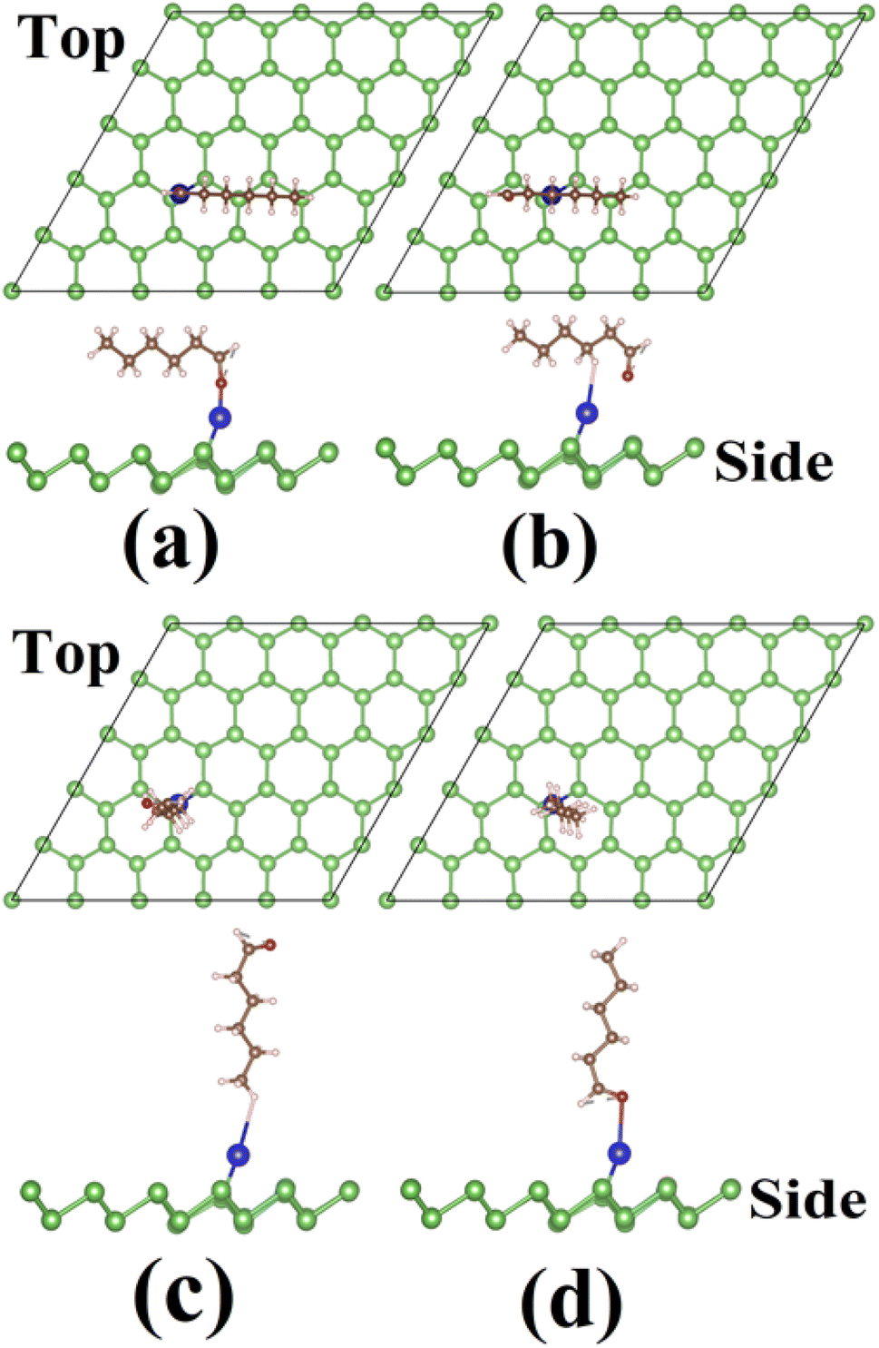 | ||
| Fig. 8 Final configuration of the hexanal molecule on Al-adsorbed arsenene (Al–As): (a) horizontal-a, (b) horizontal-b, (c) vertical-1 and (d) vertical-2. | ||
 | ||
| Fig. 9 Final configuration of the hexanal molecule on Sn-adsorbed arsenene (Sn–As): (a) horizontal-a, (b) horizontal-b, (c) vertical-1 and (d) vertical-2. | ||
 | ||
| Fig. 10 (a) TDOS, (b) DOS of the hexanal molecule (C6H12O) on Al-decorated arsenene, (c) PDOS of the As atom and C6H12O, (d) ODOS of the As atom, (e) ODOS of the Al atom and (f) ODOS of the O atom. The Fermi level (EF) is set at 0 eV. | ||
4. Conclusion
In this work, DFT calculations were performed to explore the effect of X atom (X = Al or Sn) decoration on the geometry, electronic structure, magnetism, and adsorption properties of arsenene. The Al/Sn atoms strongly bind with the arsenene surface through ionic and covalent interactions. Unlike the pristine system, both X–As molecules exhibit magnetism, mainly driven by the X atom and neighboring As atoms. Al–As presents a metallic band structure, whereas Sn–As shows a small band gap of 0.2 eV. A weak interaction was observed in the adsorption of HL on arsenene and Sn–As, leading to physisorption. However, the molecule is chemically adsorbed on Al–As, forming a chemical bond between the Al atom and the O atom of the molecule owing to the overlapping of Al-3p and O-2p orbitals. The adsorbed molecule acts as a charge acceptor. It deforms the actual charge distribution of Al–As, which may alter the transport properties of Al–As and make it suitable for HL detection.Ethical statement
The research did not involve human participants or animals.Data availability
The data generated/used in the work can be made available from the corresponding author upon reasonable request.Conflicts of interest
The authors declare no conflict of interest.Acknowledgements
The authors express their gratitude to Princess Nourah bint Abdulrahman University Researchers Supporting Project number (PNURSP2025R61), Princess Nourah bint Abdulrahman University, Riyadh, Saudi Arabia.References
- H. J. Yoon, D. H. Jun, J. H. Yang, Z. Zhou, S. S. Yang and M. M.-C. Cheng, Carbon dioxide gas sensor using a graphene sheet, Sens. Actuators, B, 2011, 157, 310–313 CAS.
- R. Kumar, N. Goel and M. Kumar, UV-Activated MoS2 Based Fast and Reversible NO2 Sensor at Room Temperature, ACS Sens., 2017, 2, 1744–1752 CrossRef CAS PubMed.
- Y. Kim, S.-K. Kang, N.-C. Oh, H.-D. Lee, S.-M. Lee and J. Park, et al., Improved Sensitivity in Schottky Contacted Two-Dimensional MoS2 Gas Sensor, ACS Appl. Mater. Interfaces, 2019, 11, 38902–38909 Search PubMed.
- M. Kunaseth, P. Poldorn, A. Junkeaw, J. Meeprasert, C. Rungnim and S. Namuangruk, et al., A DFT study of volatile organic compounds adsorption on transition metal deposited graphene, Appl. Surf. Sci., 2017, 396, 1712–1718 CAS.
- V. B. T. Phung, T. N. Tran, Q. H. Tran, T. T. Luong and V. A. Dinh, Graphene as a Sensor for Lung Cancer: Insights into Adsorption of VOCs Using vdW DFT, ACS Omega, 2024, 9, 2302–2313 CAS.
- J. Wu, Z. Li, A. Luo and X. Xing, A DFT Study of Volatile Organic Compounds Detection on Pristine and Pt-Decorated SnS Monolayers, Sensors, 2023, 23, 7319 CAS.
- R. Rahimi and M. Solimannejad, Exploring the adsorption behavior of O-containing VOCs in human breath on a B2N monolayer using DFT simulations, Phys. Chem. Chem. Phys., 2024, 26, 25567–25580 CAS.
- X. Jiang and X. Luo, BC6N Monolayer as a Potential VOC Adsorbent in Mitigation of Environmental Pollution: A Theoretical Perspective, ACS Omega, 2023, 8, 46841–46850 CAS.
- H. Farrokhpour, M. Gerami and H. Jouypazadeh, Be2C monolayer as an efficient adsorbent of toxic volatile organic compounds: theoretical investigation, Mol. Phys., 2022, 120, e2132184 Search PubMed.
- H. T. Nguyen and V. O. Vo, Adsorptio1n of VOCs onto Single Vacancy Defected Germanene Monolayer: a Study on Their Structure and Electronic Properties by DFT Calculations, Pol. J. Environ. Stud., 2023, 32, 3255–3265 CAS.
- Y. Liu, C. Ye, H. Zhao, K. Lin, X. Cao and Y. Ai, Si-Doped Nitrogenated Holey Graphene (C2N) as a Promising Gas Sensor for O-Containing Volatile Organic Compounds (VOCs) and Ammonia, Crystals, 2023, 13, 816 Search PubMed.
- C. Kamal and M. Ezawa, Arsenene: Two-dimensional buckled and puckered honeycomb arsenic systems, Phys. Rev. B:Condens. Matter Mater. Phys., 2015, 91, 085423 Search PubMed.
- Z. Zhu, J. Guan and D. Tománek, Strain-induced metal-semiconductor transition in monolayers and bilayers of gray arsenic: A computational study, Phys. Rev. B:Condens. Matter Mater. Phys., 2015, 91, 161404 Search PubMed.
- J. Shah, W. Wang, H. M. Sohail and R. I. G. Uhrberg, Experimental evidence of monolayer arsenene: an exotic 2D semiconducting material, 2D Materials, 2020, 7, 025013 CrossRef CAS.
- G. Kresse and J. Furthmüller, Efficient iterative schemes for ab initio total-energy calculations using a plane-wave basis set, Phys. Rev. B:Condens. Matter Mater. Phys., 1996, 54, 11169–11186 Search PubMed.
- J. P. Perdew, K. Burke and M. Ernzerhof, Generalized Gradient Approximation Made Simple, Phys. Rev. Lett., 1996, 77, 3865–3868 CrossRef CAS PubMed.
- S. Grimme, J. Antony, S. Ehrlich and H. Krieg, A consistent and accurate ab initio parametrization of density functional dispersion correction (DFT-D) for the 94 elements H-Pu, J. Chem. Phys., 2010, 132, 154104 Search PubMed.
- R. Nelson, C. Ertural, J. George, V. L. Deringer, G. Hautier and R. Dronskowski, Local orbital projections, atomic charges, and chemical-bonding analysis from projector-augmented-wave-based density-functional theory, J. Comput. Chem., 2020, 41, 1931–1940 CrossRef CAS PubMed.
- K. Momma and F. Izumi, VESTA 3 for three-dimensional visualization of crystal, volumetric and morphology data, J. Appl. Crystallogr., 2011, 44, 1272–1276 Search PubMed.
- V. Wang, N. Xu, J.-C. Liu, G. Tang and W.-T. Geng, VASPKIT: A user-friendly interface facilitating high-throughput computing and analysis using VASP code, Comput. Phys. Commun., 2021, 267, 108033 CrossRef CAS.
- S. Zhang, Z. Yan, Y. Li, Z. Chen and H. Zeng, Atomically Thin Arsenene and Antimonene: Semimetal–Semiconductor and Indirect–Direct Band-Gap Transitions, Angew. Chem., Int. Ed., 2015, 54, 3112–3115 CrossRef CAS PubMed.
- B. Cordero, V. Gómez, A. E. Platero-Prats, M. Revés, J. Echeverría and E. Cremades, et al., Covalent radii revisited, Dalton Trans., 2008, 2832 RSC.
Footnote |
| † Electronic supplementary information (ESI) available. See DOI: https://doi.org/10.1039/d5ra00232j |
| This journal is © The Royal Society of Chemistry 2025 |