
 Open Access Article
 This Open Access Article is licensed under a Creative Commons Attribution-Non Commercial 3.0 Unported Licence
Colloidal CuInS2 quantum well nanostructures with II–VI semiconductors as barrier layers†
Yue
Qin
 ,
Xuerong
Song
,
Hanzhuang
Zhang
,
Wenyu
Ji
* and
Jiajia
Ning
*
,
Xuerong
Song
,
Hanzhuang
Zhang
,
Wenyu
Ji
* and
Jiajia
Ning
*
Key Laboratory of Physics and Technology for Advanced Batteries (Ministry of Education), College of Physics, Jilin University, Changchun, 130012, China. E-mail: jiwy@jlu.edu.cn; jiajianing@jlu.edu.cn; qinyue20@mails.jlu.edu.cn; songxr22@mails.jlu.edu.cn; zhanghz@jlu.edu.cn
First published on 30th April 2025
Abstract
Quantum well (QW) structures have been successfully produced and utilized in high-performance optoelectronic devices. By designing QW structures at the nanoscale, it is possible to combine the advantages of both QW structures and nanostructures, resulting in extraordinary properties. In this study, a CuInS2 (CIS) quantum well layer was successfully constructed within a single nanostructure using a colloidal method. Various QW nanostructures were synthesized, including CdS/CIS/CdS, CdS/CIS/ZnS, ZnS/CIS/CdS, and Cd-free ZnS/CIS/ZnS configurations. The shapes of these QW nanostructures were precisely tuned to form tetrahedrons, hexagonal columns, and rods. Importantly, the morphology and crystal structure of the CIS layer play a crucial role in determining the final morphologies of the QW nanostructures. These QW nanostructures exhibit fluorescence emission in the near-infrared range (NIR), achieving a maximum quantum yield of 37% at 783 nm. This work demonstrates the successful construction of a CIS quantum well layer within a single colloidal nanoparticle, providing a valuable research model for fundamental studies and offering promising materials for optoelectronic devices.
Introduction
When semiconductors are combined to form heterostructures, they exhibit extraordinary properties that differ from those of single semiconductors. The semiconductor industry and its devices have been developed based on various semiconductor heterostructures. Among these structures, quantum well (QW) structures have been widely used in the industry for high-performance optoelectronic devices. QW structures typically consist of a sandwich structure, including an intermediate quantum layer and a potential barrier layer. In such structures, excitons are confined within the quantum layer, resulting in discrete energy levels, tunable emission wavelengths, and efficient electron–hole recombination.1 Generally, QW structures are formed through the deposition of different semiconductor layers, with hydride vapor phase epitaxy (HVPE), molecular beam epitaxy (MBE), and metal–organic chemical vapor deposition (MOCVD) being the most commonly used methods.2–7 The thickness of the quantum layer can be adjusted during the deposition process. Based on their compositions, various QW structures have been developed for applications in photodetectors, light-emitting diodes, and high electron mobility transistors.8–10 However, these methods pose challenges such as the need for stringent production environments, complex preparation processes, and high costs.Over the past few decades, colloidal synthetic methods have been well developed, and precise growth procedures at the atomic level have been widely applied to colloidal quantum dots (QDs) and core/shell heterostructures.11–16 The nanoparticles produced via these methods offer advantages such as low cost, easy solution-phase fabrication, and more. Precise control over growth in colloidal methods has made it possible to produce QW structures in colloidal nanostructures, such as CdS/CdSe/CdS, CdSe/HgS/CdS, and ZnSe/InP/ZnS QW nanostructures.10,11,16–18 However, compared to the well-developed colloidal QDs, the reported QW nanoparticles are limited to only a few semiconductors.11,17,19–24 Expanding the composition of colloidal QW structures to include various semiconductors remains a significant challenge in synthetic chemistry. Investigating QW nanostructures with different compositions is crucial for understanding their properties.
CuInS2 (CIS) is a low-toxicity and earth-abundant compound with an intrinsic direct bandgap of approximately 1.5 eV, making it a compelling alternative quantum layer material with a wide range of potential barrier materials. CIS QDs exhibit an electronic structure dominated by donor–acceptor pair recombination, enabling high optical performance even in nanostructured forms.25,26 Current research on CIS-based core/shell nanostructures has focused on their synthesis and properties. The optical performance of CIS in core/shell nanostructures is typically influenced by cation exchange reactions, which often result in fluorescence emission primarily in the visible region.26–29 However, the integration of CIS as a quantum layer in QW structures remains underexplored. In CIS QW structures, the light-emitting region is determined mainly by the thickness of the CIS quantum well layer, and the presence of an inner core can facilitate the growth of the CIS layer to some extent. While cation exchange still occurs, the relatively simpler experimental operation allows for more redshifted photoluminescence (PL) emission.
Herein, CuInS2 (CIS) was constructed as the interlayer for QW nanostructures. CdS/CIS/CdS QW nanostructures with tetrahedrons, hexagonal columns and rods were produced via precisely controlled ligands and precursors in colloidal synthesis. The shape and crystal structure of the CIS layer on CdS QDs are the key to tuning the shape of the final CdS/CIS/CdS QW nanostructure. The growth procedure from CdS QDs to the intermediate stage of CdS/CIS and the final CdS/CIS/CdS QW nanostructures was monitored by spectroscopy, powder X-ray diffraction (XRD) and transmission electronic microscopy (TEM) to understand the growth mechanism. CIS based QW nanostructures were further extended to Cd-free ZnS/CIS/ZnS QW nanostructures. Moreover, CdS/CIS/ZnS and ZnS/CIS/CdS QW nanostructures were also explored with a similar growth procedure. Finally, CIS based QW nanostructures exhibited fluorescence emission in the NIR range and achieved the highest PLQY of 37% at 783 nm, making these QW nanostructures promising materials for emitters and photodetectors in the NIR range. This research provides a new research model for QW nanostructures and new nanostructures for a wide range of technological innovations and applications in the field of NIR.
Results and discussion
As defined for QW structures, the exciton is confined in the QW layer due to the narrow band gap of QW layer materials. For CdS and CIS, they can form type-I (CIS/CdS core/shell) and reverse type-I (CdS/CIS core/shell) structure. If the CIS interlayer can be inserted into CdS, the CdS/CIS/CdS structure has the typical characteristics of QW structures due to the band gap alignment between CdS and CIS, as shown in Scheme 1. The band offset between CdS and CIS is 0.2 eV for the conduction band and 0.6 eV for the valence band . The wave functions of electrons and holes are confined in the CIS layer, forming a QW structure.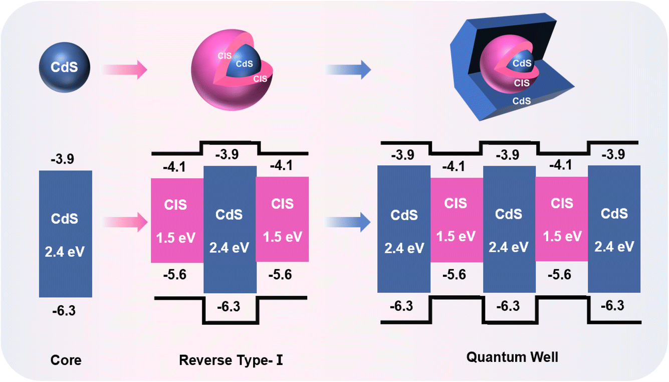 | ||
| Scheme 1 The band alignment scheme of CdS/CIS/CdS QW structures. | ||
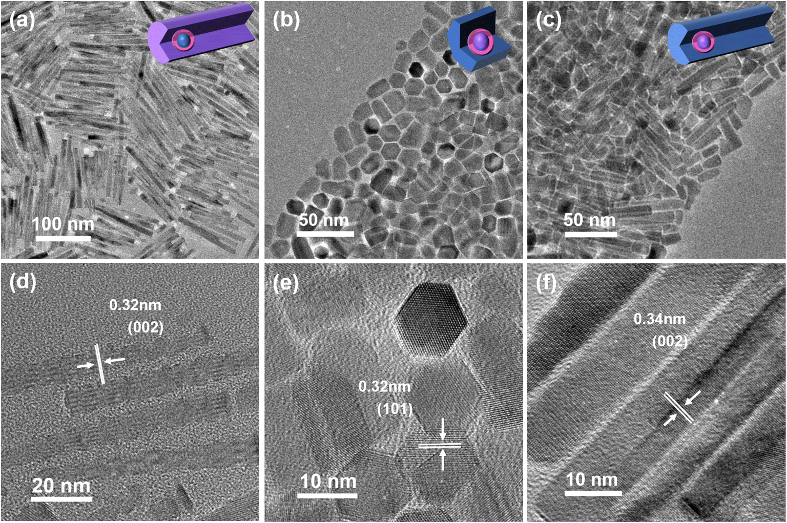
With the controlled colloidal synthetic methods from CdS QDs,30 CdS/CIS/CdS QW nanostructures were produced with different morphologies, including tetrahedrons, hexagonal columns and nanorods, as shown in Fig. 1. Tetrahedron-shaped CdS/CIS/CdS QW nanostructures have an average size of 9.5 nm (Fig. 1a and S1a†). The clear lattice in NCs indicates the single crystallinity of tetrahedron-shaped CdS/CIS/CdS QW nanostructures (Fig. 1d). The XRD pattern in Fig. S2† (navy blue line) showed distinct diffraction peaks at 26.22°, 43.61°, and 51.64°, corresponding to the cubic blende (CB) CdS (ICSD no. 97-016-8373) (Fig. S2†). As shown in Fig. S3a,† the distribution of Cd and Cu in the tetrahedron given by the line scan of one tetrahedron supports the presence of a CIS interlayer in CdS/CIS/CdS QW nanostructures. QW nanostructures for this tetrahedron-shaped CdS/CIS/CdS were further confirmed by elemental line scanning and elemental mapping in scanning transmission electron microscopy-high-angle annular dark-field imaging (AC-STEM-HADDF) and scanning transmission electron microscopy-energy dispersive spectrometer (STEM-EDS) (Fig. S4a†).
 | ||
| Fig. 1 (a) TEM image, (d) HRTEM image and (g) AC-STEM-HADDF image of tetrahedron-shaped CdS/CIS/CdS QW nanostructures, (b) TEM image, (e) HRTEM image and (h) AC-STEM-HADDF image of hexagonal column-shaped CdS/CIS/CdS QW nanostructures, and (c) TEM image, (f) HRTEM image and (i) AC-STEM-HADDF image of rod-shaped CdS/CIS/CdS QW nanostructures. The illustrated structure models for each nanostructure are shown in the inset of the TEM image, respectively. | ||
CdS/CIS/CdS QW nanostructures were also controllably synthesized into hexagonal nanocolumns and nanorods. Hexagonal nanocolumn CdS/CIS/CdS exhibit a cross-sectional length of 17.2 nm (Fig. 1b and S1b†). The single structure and the QW structure for CdS/CIS/CdS were identified from HRTEM images in Fig. 1e. The different contrast in the center of the HRTEM image indicated the core/shell structures of nanocolumns and the higher contrast was assigned to the heavy metals of Cu in the CIS quantum layer. The line scan for the elements in CdS/CIS/CdS nanocolumns in Fig. S3b† shows the responding distribution of Cu and Cd in CdS/CIS/CdS structures. AC-STEM-HADDF and STEM-EDS further confirmed the hexagonal columnar QW structure (Fig. S4b†). It is interesting that the diffraction peaks in XRD patterns (azure line in Fig. S2†) reveal a hexagonal wurtzite (WZ) crystal structure for CdS/CIS/CdS nanocolumns, different from the cubic blende (CB) for tetrahedron-shaped CdS/CIS/CdS QW nanostructures.
CdS/CIS/CdS QW nanostructures were further tuned to a rod shape (Fig. 1c) with a diameter of 8.2 nm and a length of 65.4 nm (Fig. S1c and S1d†). XRD in Fig. S2† shows the WZ structure for CdS/CIS/CdS nanorods, and the nanorods are formed along the c-axis of CdS. The measured lattice spacing of 0.34 nm in the HRTEM image (Fig. 1f) corresponds to the (002) plane of CdS, agreeing with the results obtained from XRD patterns. The HRTEM image in Fig. 1f also shows the position of the CdS/CIS core in the nanorods from the different contrast between Cd and Cu. Like the widely reported CdSe/CdS dot/rod nanostructures, CdS/CIS nanostructures acted as the starting core to form a rod-shaped CdS shell. The line scan for Cd and Cu at the tip of nanorods shows the formation of a CIS interlayer in CdS/CIS/CdS QW nanostructures (Fig. S3c†). AC-STEM-HADDF and STEM-EDS further confirmed the rod-shaped QW structure (Fig. S4b†).
Tetrahedron, hexagonal column and rod-shaped CdS/CIS/CdS QW nanostructures exhibit absorption edges around 700–900 nm in the near infrared (NIR) range, which corresponds to the enlarged band gap in the CIS layer (Fig. S5†). The difference in the absorption spectra of CdS/CIS/CdS QW nanostructures between three shapes may be induced by the various thicknesses of the CIS layer in each structure. The absorption edge from the CIS layer in absorption spectra also indicates the formation of a QW structure in CdS/CIS/CdS QW nanostructures, as shown by the band gap alignment between CdS and CIS in Scheme 1.
In the formation of tetrahedron-shaped CdS/CIS/CdS QW nanostructures, the shape and crystal structure of CdS/CIS nanostructures is the key to controlling the crystal structure and shape of the final CdS/CIS/CdS QW structure. Fig. 2 and S6† show the tetrahedral shape of CdS/CIS nanostructures when the CIS layer is grown on CdS with OLA as the ligand. The size increases from 4.7 nm to 6.4 nm for CdS, demonstrating the encapsulation of the CIS layer. The crystal structure has changed from the original cubic structure (CB) to a chalcopyrite structure (CP) (Fig. S7†). The redshift of the absorption spectrum also supports the structure of reverse type-I (Fig. 2c and S8†). This is also confirmed by the change in the band gap in the Tauc plot (Fig. S9†).
 | ||
| Fig. 2 TEM image of (a) CdS QDs and (b) tetrahedron-shaped CdS/CIS nanostructures, (c) the PL spectra of spherical CdS QDs (taro purple line), tetrahedron-shaped CdS/CIS nanostructures (pink line) and tetrahedron-shaped CdS/CIS/CdS QW nanostructures (navy blue line). | ||
When the ligands were changed to DDT and OA in the formation of the CIS layer on the same CdS QDs (Fig. 3a), the dot shape was preserved in CdS/CIS nanostructures (Fig. 3b). The increased size to 5.3 nm from the starting 4.7 nm for CdS QD supports the successful coating of the CIS layer on the surface of CdS QDs (Fig. S10†). The clear lattice in the HRTEM image for CdS/CIS nanostructures exhibits a single crystalline structure (Fig. S11†). The red shift in absorption spectra (Fig. S12†) and the emission peak (Fig. S13†) also provide evidence for the formation of CdS/CIS nanostructures. CdS/CIS nanostructures show a few diffraction peaks at 25.97°, 27.58°, 29.38°, 37.72°, 45.88°, 50.06°, and 54.76°, corresponding to the hexagonal WZ CIS structure (pink line in Fig. 4). With the spherical dot-shaped CdS/CIS nanostructures with a WZ crystal structure, the further growth of the CdS layer can form CdS/CIS/CdS QW nanostructures. When ODE-S was used as the sulfur precursor, the epitaxial growth of CdS on CdS/CIS nanostructures produced hexagonal column-shaped CdS/CIS/CdS QW nanostructures (Fig. 3c). The isotropic growth of (110) and (002) planes in WZ CdS induces the hexagonal column shape. The WZ crystal structure of the CdS shell is confirmed by XRD and HRTEM. It is interesting that a rod-shaped CdS shell was formed when DDT was used as a sulfur precursor by anisotropic growth along the c-axis (Fig. 3d). The anisotropic growth of the CdS shell along the c-axis can be attributed to the effect of DDT. This anisotropic growth is also related to the inherent polarity of the CdS/CIS structure, primarily due to the (002) plane. DDT, serving as both a sulfur source and a weak Lewis base, binds effectively to crystal planes other than the passivated (002) polar plane. Additionally, DDT has a higher affinity for Cu than for Cd, leading to an axionically terminated (002) crystal plane, which was mentioned in the previous section. This termination promotes the deposition of CdS on the polar plane, resulting in the overgrowth of the axial polar crystal planes, similar to previously reported ZnS structures.31
 | ||
| Fig. 3 TEM image of (a) CdS QDs, (b) spherical dot-shaped CdS/CIS nanostructures, (c) hexagonal column-shaped CdS/CIS/CdS QW nanostructures, and (d) rod-shaped CdS/CIS/CdS QW nanostructures. The structure models are shown in the insets of TEM images, respectively. | ||
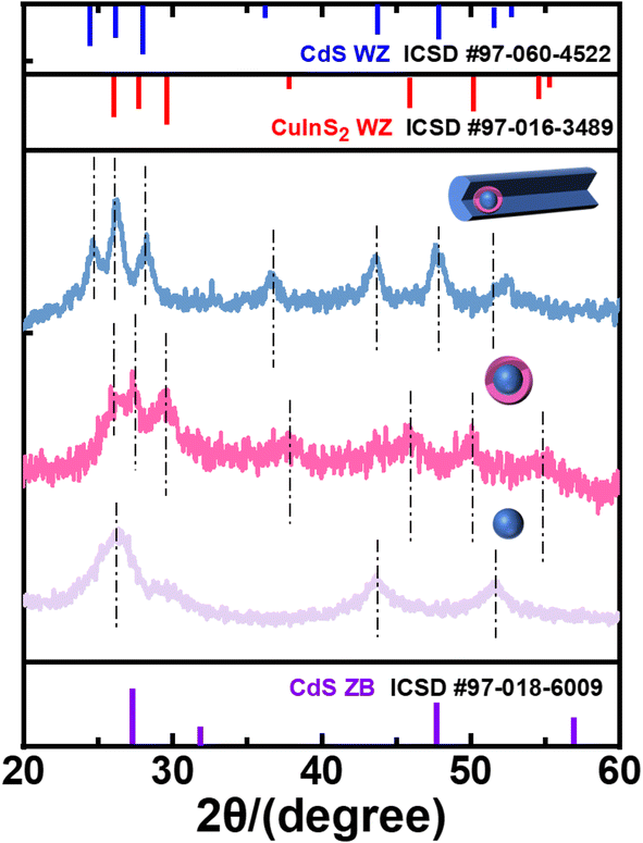 | ||
| Fig. 4 XRD patterns of CdS QDs (purple line), spherical dot-shaped CdS/CIS nanostructures (pink line) and rod-shaped CdS/CIS/CdS QW nanostructures (blue line). | ||
When DDT is used instead of OLA as the ligand, the shape of CdS/CIS changes from tetrahedral to spherical-dot and the crystal structure is tuned from CB to WZ. The ligands play a key role in turning the crystal structure and shape of the CIS layer on the surface of CdS QDs. In the synthesis of I–III–VI group QDs with OLA, the tetrahedral crystal structure of CIS and CISe governs the growth. The preferred growth of non-polar facets of the (114) plane forms tetrahedron-shaped QDs.32,33 Starting with CdS QDs having a CB crystal structure, the coating of the CIS layer on CdS QDs with OLA as the ligand was dominated by the intrinsic crystal structure of CIS to form a tetrahedron shape. However, when DDT is used as the ligand, the strong bonding between DDT and cations governs the isotropic growth to a spherical CIS layer on CdS QDs. Finally, spherical-dot shaped CdS/CIS QDs were produced. The formation of the WZ CIS layer can be attributed to the differing affinities of Cd and Cu for the ligand DDT. Cd, being a strong Lewis acid, and Cu, a weaker Lewis acid, both have a relatively better affinity for DDT, a weak Lewis base. However, as a hard Lewis base, the sulfide anion has difficulty fusing with the ligand.34,35 The presence of ODE-S promotes growth along the kinetic-dominated orientation, facilitating the generation of WZ crystal forms.
Aiming to understand the role of ligands, the growth of the CIS layer on CdS QDs was conducted without OLA and DDT ligands. Notably, the absence of these ligands resulted in irregularly elliptical/spherical nanostructures (Fig. S14†), contrasting sharply with the well-defined morphologies achieved using OLA or DDT. Despite this morphological divergence, the absorption spectra of these irregular CdS/CIS nanostructures closely matched those of spherical CdS/CIS structures (Fig. S15†), while XRD confirmed retention of the wurtzite (WZ) crystal structure (Fig. S16†). These findings underscore the pivotal role of ligands in directing nanostructure morphology, particularly highlighting DDT's function as a robust coordinating agent. The strong cation–ligand interactions (e.g., Cd/Cu-DDT binding) critically govern anisotropic growth and interfacial stability, as evidenced by the structural uniformity in ligand-assisted syntheses. This mechanistic insight establishes the foundation for precise morphological control in subsequent QW nanostructure fabrication. Additionally, the presence of a small amount of DDT ensures uniform spherical growth under WZ crystal formation conditions.32 The formation mechanism from the initial CdS QDs to CdS/CIS/CdS QW nanostructures with tetrahedrons, hexagonal columns and rods is illustrated in Scheme 2.
 | ||
| Scheme 2 The formation process of quantum well structures. | ||
As another II–VI group semiconductor, ZnS has a similar lattice to CIS. The band gap structure in ZnS can align with CIS to form type-I heterostructures. The CIS-based QW structure was extended to ZnS/CIS/ZnS QW nanostructures for Cd-free structures. The starting ZnS QDs were produced with a spherical dot shape (Fig. 5a and d) and a diameter of 2.7 nm (Fig. S17a†), showing an absorption peak at around 305 nm and a fluorescence emission peak at 360 nm (Fig. 6). The XRD patterns in Fig. S18† (blue line) show diffraction peaks that are consistent with the crystal structure of the cubic sphalerite ZnS (ICSD number 97-060-1048). Then, the CIS layer was continued to grow on ZnS QDs. After the growth of the CIS layer on ZnS QDs, the size of ZnS/CIS nanostructures becomes 5.8 nm, indicating a thickness of 1.55 nm for the CIS layer (Fig. 5b and S17b†). The HRTEM image in Fig. 5e shows a single crystalline structure for ZnS/CIS nanostructures. The measured lattice spacing of 0.32 nm corresponds to WZ CIS. Coupling with the deposition of the CIS layer on ZnS QDs, the diffraction peaks in the XRD pattern shifted to a hexagonal WZ CIS structure, which is consistent with the above part of the CdS/CIS QDs (Fig. S18†) (pink line). The significant shift in the optical spectrum with the absorption edge to around 910 nm and the fluorescence emission to 871 nm (Fig. 6) corresponds to the presence of the CIS layer on ZnS QDs.
 | ||
| Fig. 5 (a) TEM image and (d) HRTEM image of ZnS QDs, (b) TEM image and (e) HRTEM image of spherical dot-shaped ZnS/CIS nanostructures, (c) TEM image and (f) HRTEM image of rod-shaped ZnS/CIS/ZnS QW nanostructures. | ||
 | ||
| Fig. 6 Absorption and PL spectra of ZnS QDs (blue line), spherical dot-shaped ZnS/CIS nanostructures (pink line) and rod-shaped ZnS/CIS/ZnS QW nanostructures (light green line, lateral growth). | ||
ZnS was further coated on ZnS/CIS nanostructures to obtain ZnS/CIS/ZnS QW nanostructures. The produced ZnS/CIS/ZnS QW nanostructures show the shape of a rod with a diameter of 8.7 nm and a length of 57.8 nm (Fig. 5c and S17c†). The measured lattice spacing of 0.32 nm corresponds to the (002) plane in ZnS, indicating the elongated growth of ZnS along the c-axis to form a rod (Fig. 5f). The crystal structure in ZnS/CIS/ZnS QW nanorods is kept for WZ (Fig. S18†). The sharp diffraction peak at 28.18° corresponds to the anisotropic growth of the 〈002〉 crystal plane of ZnS (green line in Fig. S18†). The element line scanning for Zn and Cu supported that the rod-shaped ZnS/CIS/ZnS QW nanostructures were further confirmed by the element line scan in STEM (Fig. S19†). AC-STEM-HADDF and STEM-EDS further confirmed the rod-shaped QW structure (Fig. S20a†). The element distribution at different positions of the rod supports the formation of ZnS/CIS/ZnS QW nanostructures, and the CIS layer is at the tip of the rod. The slight blue shift of 100 nm in the emission peak was induced by the diffusion of Zn into the CIS layer during the growth of ZnS (Fig. 6). This is also confirmed by the change in the band gap in the Tauc plot (Fig. S21†).
CdS/CIS/CdS QW nanostructures with different morphologies were produced via the step-by-step deposition of a CIS layer and CdS on the starting CdS QDs. These QW nanostructures were also extended to Cd-free ZnS/CIS/ZnS QW nanostructures. The synthetic method was also tried to obtain heterostructures for the starting QDs and finally deposited materials. As shown in Fig. 7a, CdS/CIS/ZnS QW nanostructures were synthesized with starting with CdS QDs, followed by growth of ZnS on the CIS layer. CdS/CIS/ZnS QW nanostructures exhibit a rod shape with a diameter of 9.5 nm and a length of 95.5 nm (Fig. 7a and S22†). Similar to CdS/CIS/CdS rod-shaped QW nanostructures, CdS/CIS/ZnS QW nanostructures were formed by the anisotropic growth of ZnS along the c-axis on CdS/CIS nanostructures with a WZ crystal structure (Fig. S23†). The detailed growth procedure was investigated using XRD patterns and optical spectra (Fig. S23–S26†). The EDS element line scanning and AC-STEM-HADDF and STEM-EDS mapping in Fig. S20 and S27† support the formation ofCdS/CIS/ZnS QW nanostructures.
 | ||
| Fig. 7 (a) TEM image and (d) HRTEM image of rod-shaped CdS/CIS/ZnS QW nanostructures; (b) TEM image and (e) HRTEM image of hexagonal column-shaped ZnS/CIS/CdS QW nanostructures; (c) TEM image and (f) HRTEM image of rod-shaped ZnS/CIS/CdS QW nanostructures. | ||
ZnS/CIS/CdS QW nanostructures were also obtained starting with ZnS QDs, followed by the growth of CdS on ZnS/CIS nanostructures. Because of the WZ crystal structure of ZnS/CIS nanostructures (Fig. S28†), hexagonal column-shaped ZnS/CIS/CdS QW nanostructures were produced with ODE-S as the sulfur precursor and rod-shaped ZnS/CIS/CdS QW nanostructures were obtained with DDT as the sulfur precursor (Fig. 7b and c). Column-shaped ZnS/CIS/CdS QW nanostructures had a diameter of 13.0 nm (Fig. S29a†), and the QW structure was demonstrated by element line scanning in STEM by the distribution of Zn, Cu and Cd (Fig. S30†). Rod-shaped ZnS/CIS/CdS QW nanostructures were formed with the elongated growth of CdS along the 〈002〉 direction (Fig. 7f), resulting in a diameter of 8.7 nm and a length of 56.4 nm. The measured lattice spacing of 0.34 nm in HRTEM images agrees with the anisotropic growth of CdS along the c-axis. The Zn and Cu were detected at the tip of the rod by EDS element line scanning, supporting the QW structure for ZnS/CIS/CdS QW nanostructures (Fig. S31†). The growth procedure from ZnS QDs to ZnS/CIS/CdS QW nanostructures was also monitored using optical spectra, and the shift in absorption and fluorescence emission peaks corresponds to the step-by-step growth of the CIS layer and CdS (Fig. S32†).
With CdS and ZnS, the CIS layer was formed in a few colloidal nanostructures, such as CdS/CIS/CdS, ZnS/CIS/ZnS, CdS/CIS/ZnS and ZnS/CIS/CdS QW nanostructures. Because of the band alignment between CIS and CdS (ZnS), the wavefunction from excitons is confined in the CIS layer to form a QW structure (Scheme 1). The optical properties of these QW nanostructures were investigated (Fig. 8). Among these QW nanostructures, tetrahedron-shaped CdS/CIS/CdS QW nanostructures show a fluorescence emission peak at 762 nm with a PLQY of 15% (black line in Fig. 8). The Cd-free ZnS based QW nanostructures, specifically rod-shaped ZnS/CIS/ZnS QW nanostructures, show a fluorescence emission peak at 852 nm with a PLQY of 9% (blue line in Fig. 8). Compared to CdS-based and ZnS-based QW nanostructures, the hetero-QW nanostructures with CdS and ZnS together are advantageous in improving the fluorescence emission from the CIS layer. CdS/CIS/ZnS QW nanorods show fluorescence emission at 783 nm and a promoted PLQY of 37% (red line in Fig. 8). The enhanced PLQY in CdS/CIS/ZnS QW nanorods may be induced by the released strain in this un-asymmetric structure.
 | ||
| Fig. 8 PL emission spectra of CdS/CIS/CdS QW nanostructures (tetrahedron-shaped) (black line), CdS/CIS/ZnS QW nanostructures (rod-shaped) (red line), and ZnS/CIS/ZnS QW nanostructures (rod-shaped) (blue line). | ||
The Stokes shifts in different CIS QW structures were shown, and the difference in the shifts may be induced by the degree of the cation exchange reaction between Cu and Zn/Cd in various barrier layers. This phenomenon has been reported in previous studies for CIS/ZnS or CIS/CdS core/shell nanostructures.36 Due to the inherent mobility of Cu and the disparity between soft acids (Cu+, η = 6.3) and hard acids (Zn2+ or Cd2+, η = 10.9 and 10.3, respectively), cation exchange is more likely to occur in the presence of soft-base ligands such as DDT.35 Elemental line-scan data show slight overlap in the distribution of Cu and Cd/Zn, particularly at the tips of tetrahedral structures, as further validated by AC-STEM-EDS mapping (Fig. S4 and S20†). This effect appears ligand-dependent: a weakly basic ligand like OLA (compared to DDT) may exacerbate Cu+–Cd2+ exchange. Furthermore, comparative analysis of different systems (e.g., CdS/CIS/CdS, ZnS/CIS/ZnS, and CdS/CIS/ZnS) reveals that Zn–Cu exchange is more pronounced than Cd–Cu exchange. This aligns with Hard–Soft Acid–Base (HSAB) theory, as Zn2+ exhibits stronger acidity than Cd2+, creating a greater disparity with the “soft” Cu+ and thus facilitating exchange. While these effects are subtle, they could influence interfacial band structures. Combined with the data changes of PL spectra, it is also confirmed that the cation exchange occurs during multi-shell growth, and the blue shift degree of the tetrahedral cone is the largest, which also corresponds to the shift in the band gap caused by the deep degree of cation exchange.
To further elucidate the recombination mechanism in colloidal quantum wells, we selected the CdS/CIS/ZnS QW as an example to measure the PL lifetime under different excitation energies. As shown in Fig. S33,† the PL decay curve of the sample is well fitted using a double exponential function, and the average lifetime is calculated as: I(t) = A1![[thin space (1/6-em)]](https://www.rsc.org/images/entities/char_2009.gif) exp(−t/τ1) + A2exp(−t/τ2). The PL spectra for different excitation energies are shown in Fig. S34.† As described in the study, the CIS-based materials have been confirmed to exhibit donor–acceptor (D–A) pair recombination due to their large Stokes shift, broad emission linewidth, and long PL lifetime.29 The recombination probability between closer D–A pairs is significantly higher than that between distant D–A pairs. Consequently, the PL decay at higher excitation energy (350 nm) is faster than that at lower excitation (450 nm) energy, which aligns well with the characteristic features of D–A pair recombination. The PL decay behavior depends on the combined contributions of recombination from both proximal and distal D–A pairs, where the recombination of distant D–A pairs follows a slower pathway. This is consistent with the fitting results (Table S1†), showing that under high-energy excitation at 350 nm, long-range D–A pair recombination becomes more prominent, leading to a higher proportion of long-lived components and an extended average lifetime. Furthermore, the overall prolonged PL lifetime corresponds to the inherent properties of D–A pair recombination.
exp(−t/τ1) + A2exp(−t/τ2). The PL spectra for different excitation energies are shown in Fig. S34.† As described in the study, the CIS-based materials have been confirmed to exhibit donor–acceptor (D–A) pair recombination due to their large Stokes shift, broad emission linewidth, and long PL lifetime.29 The recombination probability between closer D–A pairs is significantly higher than that between distant D–A pairs. Consequently, the PL decay at higher excitation energy (350 nm) is faster than that at lower excitation (450 nm) energy, which aligns well with the characteristic features of D–A pair recombination. The PL decay behavior depends on the combined contributions of recombination from both proximal and distal D–A pairs, where the recombination of distant D–A pairs follows a slower pathway. This is consistent with the fitting results (Table S1†), showing that under high-energy excitation at 350 nm, long-range D–A pair recombination becomes more prominent, leading to a higher proportion of long-lived components and an extended average lifetime. Furthermore, the overall prolonged PL lifetime corresponds to the inherent properties of D–A pair recombination.
Conclusions
In summary, colloidal synthesis with CdS seeds was employed to construct QW nanostructures incorporating CuInS2 as an intermediate quantum layer. Precise control over the synthesis of tetrahedral, hexagonal, and rod-shaped CdS/CIS/CdS QW nanostructures was achieved by modulating the effects of OLA and OA coordination solvents and through careful addition of DDT-S and ODE-S to the sulfur precursor. The growth of CIS on CdS seeds plays a pivotal role in determining the crystal structure shape, which is strongly dependent on the selection of ligands OLA and OA. Furthermore, Cd-free ZnS/CIS/ZnS QW rod-shaped nanostructures were successfully synthesized. This growth methodology was extended to explore similar CdS/CIS/ZnS and ZnS/CIS/CdS QW nanostructures. These QW nanostructures exhibit fluorescence emission in the NIR range, with a maximum PLQY of 37% at 783 nm, attributed to the confinement of exciton wave functions within the CIS layer. This renders these QW nanostructures promising candidates for emitters and photodetectors operating in the NIR regime. In this study, the CIS QW layer was integrated within colloidal nano-QW structures, providing a novel research paradigm for both QW nanostructures and colloidal chemistry.Data availability
I am writing to submit my research paper entitled “Colloidal CuInS2 Quantum Well Nanostructures with II–VI Semiconductors as Barrier Layer” for consideration for publication in Chemical Science, authored by Yue Qin, Xuerong Song, Hanzhuang Zhang, Wenyu Ji and Jiajia Ning. We claim that “The raw data supporting the conclusions of this article will be made available by the authors, without undue reservation, to any qualified researcher.”Author contributions
J. N. and Y. Q. designed the experiments and wrote the manuscript. Y. Q. produced the nanocrystals. Y. Q. and X. S. carried out the characterization studies and analyzed the data. Y. Q., X. S., H. Z., W. J. and J. N. were involved in analyzing the results and supervising the research. H. Z., H. Z. and W. J. revised the manuscript.Conflicts of interest
The authors declare no conflict of interest.Acknowledgements
This work was supported by the National Key R&D Program of China (2022YFB3607000) and the Natural Science Foundation of Jilin Province (20220101020JC).References
- J. Joo, a. S. JSon, S. G. Kwon, J. H. Yu and T. Hyeon, Low-Temperature Solution-Phase Synthesis of Quantum Well Structured CdSe Nanoribbons, J. Am. Chem. Soc., 2006, 128, 5632–5633 CrossRef CAS PubMed.
- D. P. Dinega and M. G. Bawendi, A Solution-Phase Chemical Approach to a New Crystal Structure of Cobalt, Angew. Chem., Int. Ed., 1999, 38, 1788–1791 CrossRef CAS.
- Y. Shi, H. Li and L. J. Li, Recent advances in controlled synthesis of two-dimensional transition metal dichalcogenides via vapour deposition techniques, Chem. Soc. Rev., 2015, 44, 2744–2756 RSC.
- M. d. l. Mata, X. Zhou, F. Furtmayr, J. Teubert, S. Gradečak, M. Eickhoff, A. Fontcuberta i Morral and J. Arbiol, A review of MBE grown 0D, 1D and 2D quantum structures in a nanowire, J. Mater. Chem. C, 2013, 1, 4300–4312 RSC.
- C. L. Haynes and R. P. V. Duyne, Nanosphere Lithography: A Versatile Nanofabrication Tool for Studies of Size-Dependent Nanoparticle Optics, J. Phys. Chem. B, 2001, 105, 5599–5611 CrossRef CAS.
- C. Tabor, W. Qian and M. A. El-Sayed, Dependence of the Threshold Energy of Femtosecond Laser Ejection of Gold Nanoprisms from Quartz Substrates on the Nanoparticle Environment, J. Phys. Chem. C, 2007, 111, 8934–8941 CrossRef CAS.
- J. W. Matthews and A. E. Blakeslee, Defects in epitaxial multilayers, J. Cryst. Growth, 1976, 32, 265–273 CrossRef CAS.
- Z. Li and X. Peng, Size/shape-controlled synthesis of colloidal CdSe quantum disks: ligand and temperature effects, J. Am. Chem. Soc., 2011, 133, 6578–6586 CrossRef CAS PubMed.
- S. Hu, F. Shabani, B. Liu, L. Zhang, M. Guo, G. Lu, Z. Zhou, J. Wang, J. C. Huang, Y. Min, Q. Xue, H. V. Demir and C. Liu, High-Performance Deep Red Colloidal Quantum Well Light-Emitting Diodes Enabled by the Understanding of Charge Dynamics, ACS Nano, 2022, 16, 10840–10851 CrossRef CAS.
- A. A. Marder, J. Cassidy, D. Harankahage, J. Beavon, L. Gutiérrez-Arzaluz, O. F. Mohammed, A. Mishra, A. C. Adams, J. D. Slinker, Z. Hu, S. Savoy, M. Zamkov and A. V. Malko, CdS/CdSe/CdS Spherical Quantum Wells with Near-Unity Biexciton Quantum Yield for Light-Emitting-Device Applications, ACS Mater. Lett., 2023, 5, 1411–1419 CrossRef CAS.
- J. Zhang, C. Li, J. Li and X. Peng, Synthesis of CdSe/ZnSe Core/Shell and CdSe/ZnSe/ZnS Core/Shell/Shell Nanocrystals: Surface-Ligand Strain and CdSe–ZnSe Lattice Strain, Chem. Mater., 2023, 35, 7049–7059 CrossRef CAS.
- R. Ghosh Chaudhuri and S. Paria, Core/Shell Nanoparticles: Classes, Properties, Synthesis Mechanisms, Characterization, and Applications, Chem. Rev., 2011, 112, 2373–2433 CrossRef PubMed.
- Y. Ghosh, B. D. Mangum, J. L. Casson, D. J. Williams, H. Htoon and J. A. Hollingsworth, New insights into the complexities of shell growth and the strong influence of particle volume in nonblinking "giant" core/shell nanocrystal quantum dots, J. Am. Chem. Soc., 2012, 134, 9634–9643 CrossRef CAS PubMed.
- Z. Long, M. Liu, X.-g. Wu, K. Gu, G. Yang, Z. Chen, Y. Liu, R. Liu and H. Zhong, A reactivity-controlled epitaxial growth strategy for synthesizing large nanocrystals, Nat. Synth., 2023, 2, 296–304 CrossRef CAS.
- P. Reiss, M. Protière and L. Li, Core/Shell Semiconductor Nanocrystals, Small, 2009, 5, 154–168 CrossRef CAS PubMed.
- S. Kim, J. Park, T. Kim, E. Jang, S. Jun, H. Jang, B. Kim and S. W. Kim, Reverse type-I ZnSe/InP/ZnS core/shell/shell nanocrystals: cadmium-free quantum dots for visible luminescence, Small, 2011, 7, 70–73 CrossRef CAS PubMed.
- K. Cao, B. Yu, F. Huang, Q. Pan, J. Wang, J. Ning, K. Zheng, T. Pullerits and J. Tian, Constructing ZnTe Spherical Quantum Well for Efficient Light Emission, Nano Lett., 2024, 24, 5238–5245 CrossRef CAS.
- V. Sayevich, Z. L. Robinson, Y. Kim, O. V. Kozlov, H. Jung, T. Nakotte, Y. S. Park and V. I. Klimov, Highly versatile near-infrared emitters based on an atomically defined HgS interlayer embedded into a CdSe/CdS quantum dot, Nat. Nanotechnol., 2021, 16, 673–679 CrossRef CAS PubMed.
- S. Kim, J.-A. Kim, T. Kim, H. Chung, S. Park, S.-M. Choi, H.-M. Kim, D.-Y. Chung and E. Jang, Efficient Blue-Light-Emitting Cd-Free Colloidal Quantum Well and Its Application in Electroluminescent Devices, Chem. Mater., 2020, 32, 5200–5207 CrossRef CAS.
- G. Nagamine, B. G. Jeong, T. A. C. Ferreira, J. H. Chang, K. Park, D. C. Lee, W. K. Bae and L. A. Padilha, Efficient Optical Gain in Spherical Quantum Wells Enabled by Engineering Biexciton Interactions, ACS Photonics, 2020, 7, 2252–2264 CrossRef CAS.
- J. Cassidy, B. T. Diroll, N. Mondal, D. B. Berkinsky, K. Zhao, D. Harankahage, D. Porotnikov, R. Gately, D. Khon, A. Proppe, M. G. Bawendi, R. D. Schaller, A. V. Malko and M. Zamkov, Quantum Shells Boost the Optical Gain of Lasing Media, ACS Nano, 2022, 16, 3017–3026 CrossRef CAS PubMed.
- N. Kholmicheva, D. S. Budkina, J. Cassidy, D. Porotnikov, D. Harankahage, A. Boddy, M. Galindo, D. Khon, A. N. Tarnovsky and M. Zamkov, Sustained Biexciton Populations in Nanoshell Quantum Dots, ACS Photonics, 2019, 6, 1041–1050 CrossRef CAS.
- G. Ba, Y. Yang, F. Huang, J. Wang, Y. Lu, J. Li, C. Cheng, M. Sui and J. Tian, Gradient Alloy Shell Enabling Colloidal Quantum Wells Light-Emitting Diodes with Efficiency Exceeding 22%, Nano Lett., 2024, 24, 4454–4461 CrossRef CAS PubMed.
- T. Zhang, L. Wang, R. Jiang, Z. Wu, Y. Han, B. Xu, X. Jin, Q. Li and J. Bai, Well-type thick-shell quantum dots combined with double hole transport layers device structure assisted realization of high-performance quantum dot light-emitting diodes, Opt. Express, 2024, 32, 20618–20628 CrossRef PubMed.
- L. De Trizio, M. Prato, A. Genovese, A. Casu, M. Povia, R. Simonutti, M. J. P. Alcocer, C. D'Andrea, F. Tassone and L. Manna, Strongly Fluorescent Quaternary Cu–In–Zn–S Nanocrystals Prepared from Cu1-xInS2 Nanocrystals by Partial Cation Exchange, Chem. Mater., 2012, 24, 2400–2406 CrossRef CAS.
- L. Li, A. Pandey, D. J. Werder, B. P. Khanal, J. M. Pietryga and V. I. Klimov, Efficient synthesis of highly luminescent copper indium sulfide-based core/shell nanocrystals with surprisingly long-lived emission, J. Am. Chem. Soc., 2011, 133, 1176–1179 CrossRef CAS PubMed.
- J. Park and S.-W. Kim, CuInS2/ZnS core/shell quantum dots by cation exchange and their blue-shifted photoluminescence, J. Mater. Chem., 2011, 21, 3745–3750 RSC.
- Z. Guan, H. Ye, P. Lv, L. Wang, J. Zhang, B. Zou and A. Tang, The formation process of five-component Cu–In–Zn–Se–S nanocrystals from ternary Cu–In–S and quaternary Cu–In–Se–S nanocrystals via gradually induced synthesis, J. Mater. Chem. C, 2021, 9, 8537–8544 RSC.
- D. H. Jara, K. G. Stamplecoskie and P. V. Kamat, Two Distinct Transitions in Cu(x)InS2 Quantum Dots. Bandgap versus Sub-Bandgap Excitations in Copper-Deficient Structures, J. Phys. Chem. Lett., 2016, 7, 1452–1459 CrossRef CAS PubMed.
- W. W. Yu and X. Peng, Formation of High-Quality CdS and Other II–VI Semiconductor Nanocrystals in Noncoordinating Solvents: Tunable Reactivity of Monomers, Angew. Chem., Int. Ed., 2002, 114, 2474–2477 CrossRef.
- B. G. Jeong, Y. S. Park, J. H. Chang, I. Cho, J. K. Kim, H. Kim, K. Char, J. Cho, V. I. Klimov, P. Park, D. C. Lee and W. K. Bae, Colloidal Spherical Quantum Wells with Near-Unity Photoluminescence Quantum Yield and Suppressed Blinking, ACS Nano, 2016, 10, 9297–9305 CrossRef CAS PubMed.
- Y. Qin, X. Song, H. Zhang, H. Zhu, W. Ji and J. Ning, Growth of Ultrathick CuInS2 Shells for Supersized Core/Shell Nanoparticles, Inorg. Chem., 2024, 63, 23411–23420 CrossRef CAS PubMed.
- B. Koo, R. N. Patel and B. A. Korgel, Synthesis of CuInSe2 Nanocrystals with Trigonal Pyramidal Shape, J. Am. Chem. Soc., 2009, 131, 3134–3135 CrossRef CAS PubMed.
- R. G. Pearson, Absolute Electronegativity and Hardness: Application to Inorganic Chemistry, Inorg. Chem., 1988, 27, 734–740 CrossRef CAS.
- L. De Trizio and L. Manna, Forging Colloidal Nanostructures via Cation Exchange Reactions, Chem. Rev., 2016, 116, 10852–10887 CrossRef CAS.
- P. K. Santra, R. Viswanatha, S. M. Daniels, N. L. Pickett, J. M. Smith, P. O'Brien and D. D. Sarma, Investigation of the Internal Heterostructure of Highly Luminescent Quantum Dot−Quantum Well Nanocrystals, J. Am. Chem. Soc., 2009, 131, 470–477 CrossRef CAS.
Footnote |
| † Electronic supplementary information (ESI) available. See DOI: https://doi.org/10.1039/d5sc00657k |
| This journal is © The Royal Society of Chemistry 2025 |