
 Open Access Article
 This Open Access Article is licensed under a Creative Commons Attribution-Non Commercial 3.0 Unported Licence
High-resolution structure of Zn3(HOTP)2 (HOTP = hexaoxidotriphenylene), a three-dimensional conductive MOF†
Kimberly J.
Zhang
 a,
Tianyang
Chen
a,
Julius J.
Oppenheim
a,
Luming
Yang
b,
Lukáš
Palatinus
c,
Peter
Müller
a,
Troy
Van Voorhis
a and
Mircea
Dincă
*a
a,
Tianyang
Chen
a,
Julius J.
Oppenheim
a,
Luming
Yang
b,
Lukáš
Palatinus
c,
Peter
Müller
a,
Troy
Van Voorhis
a and
Mircea
Dincă
*a
aDepartment of Chemistry, Massachusetts Institute of Technology, 77 Massachusetts Avenue, Cambridge, Massachusetts 02139, USA. E-mail: mdinca@mit.edu
bResearch Group Electron-Spin Resonance Spectroscopy, Max Planck Institute for Multidisciplinary Sciences, Am Fassberg 11, 37077 Göttingen, Germany
cInstitute of Physics of the Czech Academy of Sciences, Na Slovance 1999/2, 18200 Prague, Czechia
First published on 2nd June 2025
Abstract
Although two-dimensional (2D) electrically conducting metal–organic frameworks (cMOFs) have become prominent due to their numerous potential applications, their structures are often implied or assumed from rather crude powder X-ray diffraction data. Indeed, exceedingly few examples exist of atomic-level structural details coming from single crystal diffraction experiments. Most widely studied among cMOFs are materials based on triphenylene ligands, in particular M3(HOTP)2 (M = Cu, Zn) and [M3(HOTP)2][M3(HOTP)]2 (M = Mg, Ni, Co; H6HOTP = 2,3,6,7,10,11-hexahydroxytriphenylene), which are invariably described as 2D van der Waals materials with sheets of ligands connected by square planar or octahedral metal ions. Here, we employ electron diffraction to show that, unlike the Mg, Co, Ni, and Cu analogs, Zn3(HOTP)2 crystallizes into a three-dimensional network that is analogous to the structures of the lanthanide-based HOTP MOFs. Moreover, similar to the lanthanide frameworks, Zn3(HOTP)2 exhibits incommensurate modulation, likely originating from a frustration between the preferred π–π stacking distance and the Zn–O bond lengths, or from a Peierls distortion. This work reinforces the importance of employing single crystal diffraction measurements for the characterization of conductive MOFs, especially when trying to correlate electronic properties to structural details.
Introduction
Owing to their unusual combination of electrical conductivity and porosity, conducting metal–organic frameworks (cMOFs) are of particular interest for a wide range of applications, from energy storage to chemiresistive sensing.1,2 Many cMOFs utilize close π–π stacking contacts and metal-semiquinone (as well as diimino- and dithioquinone) moieties to achieve high conductivity, as both facilitate long-range electron delocalization.3–9 The most prominent ones are the family of cMOFs made by reacting 2,3,6,7,10,11-hexahydroxytriphenylene (H6HOTP) with various divalent metal ions, M = Mg, Co, Ni, Cu.10–13 These frameworks crystallize as two-dimensional hexagonal nets where the metals adopt a square-planar or octahedral geometry with two semiquinone ligands (with additional pore filling M3HOTP clusters in the case of M = Mg, Ni, and Co). The hexagonal sheets can stack in a variety of arrangements, including eclipsed, slipped parallel, staggered, or more complex sequences.By analogy with the other divalent metal-based MOFs in this family, Zn3(HOTP)2 has also been assumed to adopt the same 2D stacked-sheet structure as other transition metals, with the only debate over the precise stacking arrangement of the 2D sheets.14–16 The first report of Zn3(HOTP)2 was assumed to be isostructural to Cu3(HOTP)2.14 A later report of Zn3(HOTP)2 used Rietveld refinement of powder X-ray diffraction (PXRD) data to propose eclipsed stacking of two-dimensional hexagonal nets with Zn2+ adopting square planar geometry (Fig. 1a).15 However, as is often the case with this family of materials, powder X-ray diffractograms of Zn3(HOTP)2 contain an insufficient number of reflections to allow unambiguous indexing and refinement. This original proposed structure was deemed consistent with the observed high electronic conductivity of the material due to the presence of close π–π stacking contacts.15 A subsequent report, supported by Pawley refinement of PXRD data, argued for a staggered stacking of two-dimensional hexagonal nets, which allowed for an octahedral geometry around the Zn2+ ions with water occupying the axial positions (Fig. 1a).16 The precise structure of Zn3(HOTP)2 remained unresolved due to the inherent limitations of PXRD in distinguishing between plausible stacking arrangement and coordination geometries (Fig. 1b and S1†).
 | ||
| Fig. 1 (a) In previous studies, simulated models of Zn3(HOTP)2 depict square-planar or octahedral Zn2+ ions (purple) linking HOTP ligands (dark hexagons with red O atoms) in parallel 2D hexagonal layers stacked along the c-axis. (b) In this work, diffraction studies establish Zn3(HOTP)2 as a lattice wherein Zn2+ nodes bridge HOTP linkers into a three-dimensional framework where neighboring HOTP ligands are not coplanar. The connectivity and Zn2+ coordination environments differ significantly, highlighting the importance of direct structural characterization. | ||
Results and discussion
The debate over the structure of Zn3(HOTP)2 is not just a question of crystallography: the relative orientation of individual sheets in 2D electronic materials has profound consequences on their bulk electronic structures.17,18 To resolve this debate, we sought to produce sufficiently large crystals of Zn3(HOTP)2 to allow structural determination by single crystal diffraction. Solvothermal reaction of H6HOTP with Zn(OAc)2·2H2O in a mixture of water and N,N-dimethylformamide (DMF) yields Zn3(HOTP)2 as a dark-blue crystalline powder (Fig. 2a). Activation of this material by desolvation under dynamic vacuum, followed by an N2 adsorption isotherm at 77 K, gave an apparent Brunauer–Emmett–Teller (BET) surface area of 249.9 m2 g−1 (Fig. S2†), in line with previously reported values of 274 to 330 m2 g−1.15,16 Morphologically, crystallites of Zn3(HOTP)2 present as approximately 2 μm long needles with a hexagonal cross-section measuring approximately 600 nm (Fig. 2e). Further details on physical characterization, including elemental analysis, thermogravimetric analysis, and UV-vis spectroscopy, are provided in the ESI (Fig. S3–S5†). Although too small for single crystal X-ray diffraction, these crystals were suitable for characterization by electron diffraction.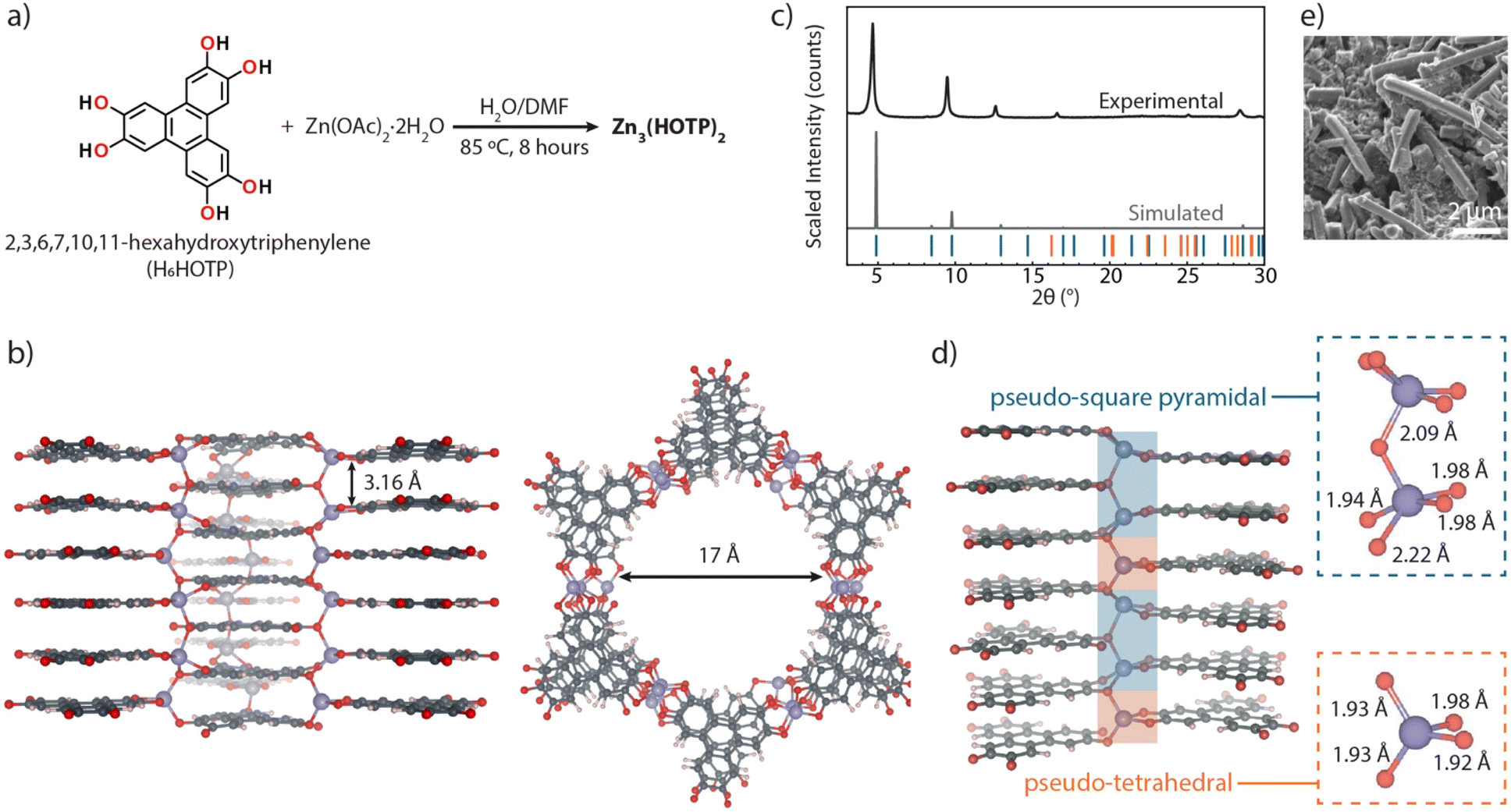 | ||
| Fig. 2 Structural characterization of Zn3(HOTP)2: (a) synthetic route to Zn3(HOTP)2via solvothermal reaction of H6HOTP and Zn(OAc)2·2H2O in H2O/DMF at 85 °C. (b) Crystal structure of Zn3(HOTP)2 viewed down the a*-axis (left) showing 1D channels (highlighting offset π-stacking with a 3.16 Å stacking distance) and down the c-axis (right) (the interatomic distance across the pore is ∼17 Å). (c) Experimental PXRD of Zn3(HOTP)2 with simulated PXRD data. The blue ticks denote main reflections and orange ticks denote first order satellite reflections (d) structural views of the commensurate approximant model, showing Zn2+ ions in pseudo-square pyramidal (blue) and pseudo-tetrahedral (orange) geometries with corresponding Zn–O bond lengths. (e) SEM image of Zn3(HOTP)2 crystallites showing ∼2 μm needles with hexagonal cross-sections. | ||
Data obtained from 3D electron diffraction (3D ED, also known as MicroED) revealed that Zn3(HOTP)2 crystallizes in the super-space group P63/mmc(00γ)00ss with lattice parameters a = b = 20.866 Å and a rather short π-stacking distance that coincides with the c unit cell parameter of 3.1649 Å, with a modulating vector q = 0.3488c* (Table S1 and Fig. S6–S17†). Although a view parallel to the c direction reveals the expected honeycomb structure with an interatomic distance across the pore of ∼17 Å and a calculated pore diameter of ∼14 Å (Fig. S2†), views along the a or b directions show that the organic ligands do not form continuous coplanar 2D sheets, as is the case with other transition metals (Fig. 2b). Further, the Zn2+ ions do not adopt a square planar arrangement and, most importantly, are not bound to just two catecholate ligands, as is the case with other divalent ions in the M3(HOTP)2 family. Instead, two crystallographically independent Zn2+ ions adopt 4-coordinate pseudo-Td and 5-coordinate pseudo-C4v geometries, each coordinating to three independent HOTP ligands (Fig. 2d). Although the HOTP ligands define π-stacking columns, neighbouring columns are offset by half a unit cell in the c direction, such that there are no 2D continuous, coplanar sheets of organic ligands (Fig. 2d). Because the Zn2+ ions connect HOTP ligands in the c direction, Zn3(HOTP)2 is therefore a three-dimensional MOF, not a 2D one as previously assumed. In this sense, it is similar to, but not isostructural with the lanthanide-HOTP MOFs, wherein lanthanide ions situated between organic layers connect HOTP ligands in the third direction.19
Another resemblance with the lanthanide-HOTP MOFs structures is the incommensurate modulation found in Zn3(HOTP)2. This modulation leads to a variation of the position of the Zn nodes along the c direction relative to HOTP linkers. We note that, because the modulation vector is close to 1/3, the structure can be approximated as a 3-fold supercell. The supercell corresponds to space group P![[6 with combining macron]](https://www.rsc.org/images/entities/char_0036_0304.gif) with a c-lattice parameter of 9.49 Å (with each π–π stacking distance of 3.16 Å) and 3 coordinatively saturated Zn2+ ions per unit cell sitting on two pseudo-C4v sites and one pseudo-Td site. The Zn ions do not lie directly on the 2-fold rotation axis and are resultantly disordered over two positions. The occupancy of Zn ions in these sites has a discontinuous occupational modulation. This positional disorder and modulation are correlated to the disorder and modulation of a rotation of the HOTP linker in the ab plane. For both the Zn and lanthanide-HOTP frameworks, the modulation can be seen as originating from either a geometric frustration between the preferred π–π stacking distance and the metal–oxygen bond length, or from a Peierls distortion wherein the one-dimensional band formed by the π-stacked HOTP is partially filled (due to linker oxidation).19 The observation of incommensurate modulation in Zn3(HOTP)2 raises the intriguing possibility of a charge-density wave (CDW) state, as seen in the Ln-HOTP analog.20 While further experiments are needed to probe this hypothesis, Zn3(HOTP)2 joins the class of incommensurately modulated MOFs with potential for electronically driven structural transitions.
with a c-lattice parameter of 9.49 Å (with each π–π stacking distance of 3.16 Å) and 3 coordinatively saturated Zn2+ ions per unit cell sitting on two pseudo-C4v sites and one pseudo-Td site. The Zn ions do not lie directly on the 2-fold rotation axis and are resultantly disordered over two positions. The occupancy of Zn ions in these sites has a discontinuous occupational modulation. This positional disorder and modulation are correlated to the disorder and modulation of a rotation of the HOTP linker in the ab plane. For both the Zn and lanthanide-HOTP frameworks, the modulation can be seen as originating from either a geometric frustration between the preferred π–π stacking distance and the metal–oxygen bond length, or from a Peierls distortion wherein the one-dimensional band formed by the π-stacked HOTP is partially filled (due to linker oxidation).19 The observation of incommensurate modulation in Zn3(HOTP)2 raises the intriguing possibility of a charge-density wave (CDW) state, as seen in the Ln-HOTP analog.20 While further experiments are needed to probe this hypothesis, Zn3(HOTP)2 joins the class of incommensurately modulated MOFs with potential for electronically driven structural transitions.
To obtain more insight into the electronic structure of Zn3(HOTP)2, we performed density functional theory (DFT) calculations at the HSE06 level on the 3-fold commensurate approximant (Fig. 3 and Table S2†).21 We find that along the Γ-A pathway in the Brillouin zone (corresponding to the real-space c-direction) there is a large band curvature, where the band, formed by the HOTP-linker HOMO and HOMO-1 orbitals, crosses the Fermi level. This is consistent with a large amount of π–π overlap between HOTP linkers. Along the Γ–M–K pathway (corresponding to the ab plane), the bands are flat with a small band gap of ∼0.1 eV. The flat band is consistent with electrons that cannot delocalize from the HOTP linkers to the Zn due to high ionicity and low orbital overlap. From this, Zn3(HOTP)2 should be semi-conductive in the ab plane and metallic along the c-vector. Consistent with a highly ionic Zn, the species-projected density-of-states (pDOS) reveals that the bands around the Fermi level are populated only by the valence orbitals of carbon and oxygen (i.e., the HOTP linker).
 | ||
| Fig. 3 Calculated band structure with projected density of states (DOS) of Zn3(HOTP)2. The inset shows the first Brillouin zone of the material with high symmetry k-points. Zn3(HOTP)2 has a small band gap in the in-plane direction, and significant band curvature is observed in the out-of-plane direction. Zn3(HOTP)2 is calculated to be metallic, as demonstrated by the band crossing the Fermi-level in the out-of-plane direction, and a non-zero projected DOS at the Fermi-level. | ||
In our hands, polycrystalline pressed pellets of Zn3(HOTP)2 exhibit an average two-contact probe conductivity of 2.05 × 10⁻⁵ S cm−1 and highest conductivity of 5.4 × 10⁻⁵ S cm−1 (Fig. S18†). These values are in line with the original reported conductivity for Zn3(HOTP)2, 8 × 10⁻⁵ S cm−1,15 but nearly 1000 times lower than the later reported value of 4.5 × 10⁻² S cm−1,16 which has a significantly different synthetic procedure than the one we used. We note here that two-contact probe measurement possesses significant contact resistance, which might explain the discrepancies of our measured conductivity with that of the reported ones. As well, different particle morphologies produced for each procedure will lead to different crystallite packings, affecting the grain boundary resistances. We also acknowledge the likelihood that different synthetic conditions may lead to the formation of a Zn3(HOTP)2 phase that is indeed 2D (Fig. S1†), which could potentially have higher conductivity.
To better understand the intrinsic electronic transport properties and eliminate contact resistance effects, we performed four-probe conductivity measurements on pellets pressed under different pressures. At 3 tons of pressure, the conductivity was 3.36 × 10⁻⁵ S cm−1; when increased to 6 and 9 tons, it rose to 7.78 × 10⁻⁵ S cm−1 and 1.04 × 10⁻⁴ S cm−1, respectively (Table 1). The increase in conductivity at higher packings is consistent with a decrease in the contribution of grain boundary resistances. However, given that the band structure calculations predict metallic transport (along the c direction) and ∼10−4 S cm−1 is too resistive to be consistent with metallic transport, the grain boundary resistances must still dominate the device conductivity. In addition, the highly anisotropic nature of charge transport in Zn3(HOTP)2 and the large aspect ratio of needle-like crystals suggest that the conductivity of the pellet may also depend on the average orientation of the crystals. These observations are consistent with that for the Ln-HOTP MOFs, where the single crystal conductivity is ∼1000 S cm−1 along the c-direction but the pressed pellet conductivity is only ∼10−4 S cm−1.19,20
| Method | Pressure (tons) | Conductivity (S cm−1) |
|---|---|---|
| Four-probe | 3 | 3.36 × 10⁻⁵ |
| Four-probe | 6 | 7.78 × 10⁻⁵ |
| Four-probe | 9 | 1.04 × 10⁻⁴ |
Alternatively, if the cause of the modulation is indeed a CDW state, we might expect the appearance of a band gap at the wavevector q = 0.3488c*, whereas for the calculated commensurate approximant q = 1/3c*, there would be no band gap. Thus, the calculation would predict metallic behavior for the approximant, whereas the CDW state could be semiconducting.
Conclusions
In conclusion, we have reported the single crystal structure of Zn3(HOTP)2 determined by electron diffraction. Notably, this MOF adopts a three-dimensional connected topology whereby the Zn ions bridge between π–π stacks of HOTP linkers. As well, the structure exhibits an incommensurate modulation. We hope that future work strives towards large single crystal synthesis, such that axis-oriented single crystal electronic conductivity measurements may be performed as well as variable temperature studies to determine the nature of the incommensurate modulation.Data availability
The data supporting this article have been included as part of the ESI.†Author contributions
K. J. Z., T. C., M. D. designed this project. K. J. Z. and L. Y. conducted materials synthesis. K. J. Z. carried out conductivity measurement, BET surface area measurement, and band structure calculations. J. J. O., L. P. and P. M. performed electron diffraction measurement and data analysis. All authors contributed to discussion, data curation and review of the manuscript. K. J. Z. and J. J. O. prepared manuscript. T. V. V. and M. D. supervised all aspects of the research.Conflicts of interest
There are no conflicts to declare.Acknowledgements
This work was funded by the Department of Energy (DE-SC0023288). K. J. Z. is partially supported by the National Science Foundation through the Graduate Research Fellowship Program (NSF-GRFP). L. P. acknowledges the support by the Czech Science Foundation, project number 21-05926X. L. P. also acknowledges the project Terafit and CzechNanoLab Research Infrastructure, both supported by MEYS CR (project numbers CZ.02.01.01/00/22_008/0004594 and LM2023051). We would like to thank the MIT International Science and Technology Initiatives (MISTI) for financial support through the MIT-Czech Republic Seed Fund.Notes and references
- D. Feng, T. Lei, M. R. Lukatskaya, J. Park, Z. Huang, M. Lee, L. Shaw, S. Chen, A. A. Yakovenko, A. Kulkarni, J. Xiao, K. Fredrickson, J. B. Tok, X. Zou, Y. Cui and Z. Bao, Robust and Conductive Two-Dimensional Metal-Organic Frameworks with Exceptionally High Volumetric and Areal Capacitance, Nat. Energy, 2018, 3(1), 30–36, DOI:10.1038/s41560-017-0044-5.
- M. Yao, X. Lv, Z. Fu, W. Li, W. Deng, G. Wu and G. Xu, Layer-by-Layer Assembled Conductive Metal–Organic Framework Nanofilms for Room-Temperature Chemiresistive Sensing, Angew. Chem., 2017, 129(52), 16737–16741, DOI:10.1002/ange.201709558.
- M. G. Campbell, D. Sheberla, S. F. Liu, T. M. Swager and M. Dincă, Cu 3 (Hexaiminotriphenylene) 2 : An Electrically Conductive 2D Metal–Organic Framework for Chemiresistive Sensing, Angew. Chem., 2015, 127(14), 4423–4426, DOI:10.1002/ange.201411854.
- S. S. Shinde, C. H. Lee, J. Y. Jung, N. K. Wagh, S. H. Kim, D. H. Kim, C. Lin, S. U. Lee and J. H. Lee, Unveiling Dual-Linkage 3D Hexaiminobenzene Metal-Organic Frameworks towards Long-Lasting Advanced Reversible Zn-Air Batteries, Energy Environ. Sci., 2019, 12(2), 727–738, 10.1039/c8ee02679c.
- D. Sheberla, L. Sun, M. A. Blood-Forsythe, S. Er, C. R. Wade, C. K. Brozek, A. Aspuru-Guzik and M. Dincă, High Electrical Conductivity in Ni3(2,3,6,7,10,11- Hexaiminotriphenylene)2, a Semiconducting Metal-Organic Graphene Analogue, J. Am. Chem. Soc., 2014, 136(25), 8859–8862, DOI:10.1021/ja502765n.
- X. Huang, P. Sheng, Z. Tu, F. Zhang, J. Wang, H. Geng, Y. Zou, C. A. Di, Y. Yi, Y. Sun, W. Xu and D. Zhu, A Two-Dimensional π-d Conjugated Coordination Polymer with Extremely High Electrical Conductivity and Ambipolar Transport Behaviour, Nat. Commun., 2015, 6, 7408, DOI:10.1038/ncomms8408.
- J. H. Dou, L. Sun, Y. Ge, W. Li, C. H. Hendon, J. Li, S. Gul, J. Yano, E. A. Stach and M. Dinca, Signature of Metallic Behavior in the Metal-Organic Frameworks M3(Hexaiminobenzene)2 (M = Ni, Cu), J. Am. Chem. Soc., 2017, 139(39), 13608–13611, DOI:10.1021/jacs.7b07234.
- R. Dong, P. Han, H. Arora, M. Ballabio, M. Karakus, Z. Zhang, C. Shekhar, P. Adler, P. S. Petkov, A. Erbe, S. C. B. Mannsfeld, C. Felser, T. Heine, M. Bonn, X. Feng and E. Cánovas, High-Mobility Band-like Charge Transport in a Semiconducting Two-Dimensional Metal–Organic Framework, Nat. Mater., 2018, 17(11), 1027–1032, DOI:10.1038/s41563-018-0189-z.
- R. W. Day, D. K. Bediako, M. Rezaee, L. R. Parent, G. Skorupskii, M. Q. Arguilla, C. H. Hendon, I. Stassen, N. C. Gianneschi, P. Kim and M. Dincă, Single Crystals of Electrically Conductive Two-Dimensional Metal-Organic Frameworks: Structural and Electrical Transport Properties, ACS Cent. Sci., 2019, 5(12), 1959–1964, DOI:10.1021/acscentsci.9b01006.
- M. Hmadeh, Z. Lu, Z. Liu, F. Gándara, H. Furukawa, S. Wan, V. Augustyn, R. Chang, L. Liao, F. Zhou, E. Perre, V. Ozolins, K. Suenaga, X. Duan, B. Dunn, Y. Yamamto, O. Terasaki and O. M. Yaghi, New Porous Crystals of Extended Metal-Catecholates, Chem. Mater., 2012, 24(18), 3511–3513, DOI:10.1021/cm301194a.
- L. S. Xie, G. Skorupskii and M. Dincă, Electrically Conductive Metal-Organic Frameworks, Chem. Rev., 2020, 26, 8536–8580, DOI:10.1021/acs.chemrev.9b00766.
- J. H. Dou, M. Q. Arguilla, Y. Luo, J. Li, W. Zhang, L. Sun, J. L. Mancuso, L. Yang, T. Chen, L. R. Parent, G. Skorupskii, N. J. Libretto, C. Sun, M. C. Yang, P. V. Dip, E. J. Brignole, J. T. Miller, J. Kong, C. H. Hendon, J. Sun and M. Dincă, Atomically Precise Single-Crystal Structures of Electrically Conducting 2D Metal–Organic Frameworks, Nat. Mater., 2021, 20(2), 222–228, DOI:10.1038/s41563-020-00847-7.
- L. Sun, L. Yang, J. H. Dou, J. Li, G. Skorupskii, M. Mardini, K. O. Tan, T. Chen, C. Sun, J. J. Oppenheim, R. G. Griffin, M. Dincă and T. Rajh, Room-Temperature Quantitative Quantum Sensing of Lithium Ions with a Radical-Embedded Metal-Organic Framework, J. Am. Chem. Soc., 2022, 144(41), 19008–19016, DOI:10.1021/jacs.2c07692.
- Y. Misumi, A. Yamaguchi, Z. Zhang, T. Matsushita, N. Wada, M. Tsuchiizu and K. Awaga, Quantum Spin Liquid State in a Two-Dimensional Semiconductive Metal–organic Framework, J. Am. Chem. Soc., 2020, 142(39), 16513–16517, DOI:10.1021/jacs.0c05472.
- Y. Chen, Q. Zhu, K. Fan, Y. Gu, M. Sun, Z. Li, C. Zhang, Y. Wu, Q. Wang, S. Xu, J. Ma, C. Wang and W. Hu, Successive Storage of Cations and Anions by Ligands of π–d-Conjugated Coordination Polymers Enabling Robust Sodium-Ion Batteries, Angew. Chem., Int. Ed., 2021, 60(34), 18769–18776, DOI:10.1002/anie.202106055.
- J. Y. Choi, M. Stodolka, N. Kim, H. T. B. Pham, B. Check and J. Park, 2D Conjugated Metal-Organic Framework as a Proton-Electron Dual Conductor, Chem, 2023, 9(1), 143–153, DOI:10.1016/j.chempr.2022.09.016.
- Y. Cao, V. Fatemi, S. Fang, K. Watanabe, T. Taniguchi, E. Kaxiras and P. Jarillo-Herrero, Unconventional Superconductivity in Magic-Angle Graphene Superlattices, Nature, 2018, 556(7699), 43–50, DOI:10.1038/nature26160.
- I. Zutić, J. Fabian and S. Das Sarma, Spintronics: Fundamentals and Applications, Rev. Mod. Phys., 2004, 76, 323, DOI:10.1103/RevModPhys.76.323.
- G. Skorupskii, B. A. Trump, T. W. Kasel, C. M. Brown, C. H. Hendon and M. Dinca, Efficient and Tunable One-Dimensional Charge Transport in Layered Lanthanide Metal–Organic Frameworks, Nat. Chem., 2020, 12(2), 131–136, DOI:10.1038/s41557-019-0372-0.
- G. Skorupskii, K. N. Le, D. L. M. Cordova, L. Yang, T. Chen, C. H. Hendon, M. Q. Arguilla and M. Dincă, Porous Lanthanide Metal-Organic Frameworks with Metallic Conductivity, Proc. Natl. Acad. Sci. U. S. A., 2022, 119(34), e2205127119, DOI:10.1073/pnas.2205127119.
- J. Paier, M. Marsman, K. Hummer, G. Kresse, I. C. Gerber and J. G. Angyan, Erratum: Screened Hybrid Density Functionals Applied to Solids, J. Chem. Phys., 2006, 124, 154709, DOI:10.1063/1.2187006.
Footnote |
| † Electronic supplementary information (ESI) available: Computational methods, electron diffraction micrographs, SEM, PXRD patterns, electrical conductivity measurement (PDF). CCDC 24091022446225. For ESI and crystallographic data in CIF or other electronic format see DOI: https://doi.org/10.1039/d5sc00894h |
| This journal is © The Royal Society of Chemistry 2025 |