
 Open Access Article
 This Open Access Article is licensed under a
 Creative Commons Attribution 3.0 Unported Licence
Unlocking the potential of semi-transparent Ta3N5 photoelectrodes for high-performance, reproducible solar redox flow cells†
Filipe Moisés M.
Francisco
 ab,
Paula
Dias
*ab and
Adélio
Mendes
*ab
ab,
Paula
Dias
*ab and
Adélio
Mendes
*ab
aLEPABE – Laboratory for Process Engineering, Environment, Biotechnology and Energy, Faculty of Engineering, University of Porto, Rua Dr Roberto Frias, 4200-465 Porto, Portugal. E-mail: pauladias@fe.up.pt; mendes@fe.up.pt
bALiCE – Associate Laboratory in Chemical Engineering, Faculty of Engineering, University of Porto, Rua Dr Roberto Frias, 4200-465 Porto, Portugal
First published on 11th March 2025
Abstract
A solar redox flow cell (SRFC) converts solar energy into storable electrochemical energy and heat; when connected to a redox flow battery, it can produce dispatchable electricity. Despite its versatility, a SRFC is still considered to be at a low technology readiness level (TRL), mainly due to the absence of abundant, efficient, and stable semiconductors. Tantalum nitride (Ta3N5) photoelectrodes have garnered special interest for photoelectrochemical water-splitting applications, particularly those using opaque Ta substrates. However, for SRFCs, which are normally based on coloured electrolytes, Ta3N5 needs to be semi-transparent to allow backside sunlight illumination. Herein, for the first time, the electrophoretic deposition technique was optimized for synthesizing semi-transparent Ta3N5. The best-performing bare photoelectrodes were prepared over a 30 nm Ta-doped TiO2 (TTO) underlayer, and with an electrophoretic time of 7 min and an annealing temperature of 425 °C in an NH3 atmosphere, displaying an unprecedented photocurrent density of ca. 4.0 mA cm−2, and a maximum power density of ca. 1.1 mW cm−2, using a ferrocyanide-based electrolyte. These conditions allowed improving the charge-transfer kinetics and reducing the recombination rates, as observed by electrochemical impedance spectroscopy analysis. The optimized Ta3N5 photoelectrode was paired with a perovskite solar cell, demonstrating ca. 100 h of operation in an aqueous alkaline electrolyte, based on ferrocyanide (K4Fe(CN)6) and anthraquinone-2,7-disulphonate (2,7-AQDS) redox pairs.
Introduction
Fossil fuels, particularly coal and oil, remain the dominant energy sources and still contribute significantly to carbon dioxide emissions and environmental degradation.1,2 Renewable energy sources, especially solar energy, offer a clean and economically feasible approach to accelerate the decarbonization of the energy system. However, harnessing solar energy efficiently poses challenges due to its intermittent nature, underscoring the need for advanced energy storage and conversion systems.Solar redox flow cells (SRFCs) represent a groundbreaking approach to address the global energy paradigm, especially combining solar energy capture, conversion, and storage in a compact device. Briefly, a SRFC combines the working principles of a photoelectrochemical (PEC) cell, capable of photocharging the redox pairs dissolved in the electrolyte, using semiconductor-based photoelectrodes, with the working principles of a redox flow cell (RFC).3 The fundamental advantage of the PEC cell is the spontaneous heterojunction formation at the semiconductor–electrolyte interface. With the proper pairing of the appropriate material and solution, the chemical potential difference between the two phases results in the formation of a built-in electric field within the semiconductor. When illuminated, the semiconductor absorbs photons with energy (hν) equal to or greater than its own energy bandgap and is thus capable of generating electron–hole (e−–h+) pairs. The excited electrons move to the conduction band (CB), leaving holes in the valence band (VB), as follows:4
| hν + semiconductor → eCB− + hVB+ | (1) |
The electrons are then transported externally to the counter electrode, where the reduction reaction takes place:
| A + hVB+ → A+ | (2) |
Simultaneously, the holes in the valence band of the semiconductor material are pushed to its surface, driving the oxidation reaction, as follows:
| B + eCB− → B− | (3) |
Therefore, the semiconductor-based photoelectrode plays an important role in the final performance of SRFCs. For reaching the highest solar energy conversion efficiencies, the valence and conduction band edges of the photoelectrode need to match with the Nernst redox potentials of the redox pairs. So far, over 1000 redox pairs have been identified as candidates for use in RFCs.5 The photocharged redox pairs can be discharged in RFCs to produce electricity; see Fig. 1. Moreover, the heat stored in the electrolytes can be heat-exchanged for sanitary water applications or for thermal comfort, which increases the overall efficiency of the SRFC system.
 | ||
| Fig. 1 Representative scheme of a solar redox flow cell (SRFC) based on a photoanode-driven PEC cell, where A is the catholyte solution, B is the anolyte solution, CB and VB are the conduction band and the valence band of the semiconductor, respectively, ΔE is the applied potential, and e− is an electron. | ||
Despite the high promise of SRFCs, the development of efficient systems has been hampered by several factors, including the scarcity of abundant and low-cost materials, the instability of highly efficient photoelectrodes, and the sluggish reaction kinetics, which often necessitate the use of complex and costly heterojunctions or catalysts.6 To overcome these limitations, identifying semiconductor materials that are earth-abundant, efficient, stable, and scalable is crucial.7 Tantalum nitride (Ta3N5) photoanodes promise high efficiencies, due to their narrow bandgap energy of ca. 2.1 eV and optimal optoelectronic properties, contrary to what happens with hematite (α-Fe2O3, a similar bandgap), one of the most studied metal-oxide photoelectrodes.8 Ta3N5 has a longer hole diffusion length, its valence band is composed of N 2p, and the bottom of the conduction band is at −0.3 VRHE, showing a more negative onset potential (0.6 V higher than α-Fe2O3), and a lower bias potential for oxidation reactions.9 These characteristics have allowed boosting its near-theoretical photocurrent limit over the past 10 years.10 A maximum photocurrent density of ca. 12.1 mA cm−2 was reported for PEC water splitting using a complex Ta3N5 thin film coated with Ni(OH)x/ferrihydrite/TiOx, and Co- and Ir-based molecular catalysts.11 However, the onset potential of this photoanode (0.6–0.7 VRHE) was still much more positive than the theoretical value, resulting in a lower photopotential; the stability was also very challenging. Moreover, this unprecedented result was obtained following the oxidation and nitrification of an opaque Ta metal foil substrate, at a high temperature (ca. 1000 °C). To obtain an unbiased high-performing SRFC, Cheng et al.12 used a Ta3N5 nanotube-structured opaque photoanode paired with a GaN nanowire/Si photocathode in 1.2 V alkaline anthraquinone/ferrocyanide redox pairs; however, the system was illuminated from both sides of the photoactive materials, leading to lower solar power conversion efficiencies. This opaque substrate only allowed illumination of the front-side of the photoactive material, and also presented reduced efficiencies when coloured electrolytes were used due to light-absorption competition through the electrolyte film. Therefore, the use of transparent conducting oxide (TCO) glass substrates, such as fluorine-doped tin oxide (FTO) and indium-doped tin oxide (ITO), is a requisite and also critical for assembling tandem arrangements. The latter configurations facilitate testing redox chemistries based on high cell potentials (>0.8 V), which are limited by the typical current low photopotentials of Ta3N5.
Electrophoretic deposition (EPD) was the first technique reported for the development of semi-transparent Ta3N5 photoanodes. Domen et al.13 reported a semi-transparent Ta3N5 film that achieved a photocurrent density of ca. 0.4 mA cm−2 at 1.3 VRHE, using 0.1 M Na2SO4 solution as the electrolyte, without any co-catalyst; the photocurrent could be increased to ca. 2.4 mA cm−2 when employing an IrO2 overlayer. Since then, several works based on EPD,14–16 and other deposition techniques, such as atomic layer deposition (ALD),17,18 have been performed with reasonable performances reported. The ALD technique allows the deposition of conformal and uniform films over any substrate with a good interconnection between molecules and atomic-level control, which is not so easy to obtain with the EPD technique. However, one of the limitations of ALD is the fact that the direct deposition of Ta3N5 on the glass substrate is not possible, but this can be overcome by replacement of the oxidizing precursor with ammonia. This presents not only some safety concerns due to the use of ammonia in high vacuum conditions, but also the deposition process must be carried out at high temperatures, therefore requiring meticulous control to ensure it does not affect the properties of the FTO underlayer.
Alternatively, EPD is a low-cost, highly efficient method to fabricate oxide- or organic-based thin films on various conductive substrates and it does not require high-temperature heat treatment. EPD is an electrochemical technique where charged colloidal particles, dispersed or suspended in a liquid medium, are attracted and deposited onto an electrically conductive substrate with opposite charges under an electric field.19 Therefore, the presence of defects on the interface of the Ta-based particles and the conductive glass substrate plays an important role in the photoelectrodes' performance, i.e. the combination between the Ta3N5 particles' surface area and the interfacial roughness of the FTO substrate creates recombination centres, which must be mitigated.20 It was reported that post-treatment with a TaCl5 methanolic solution13,14 could improve the adhesion of the Ta-based particles to each other, but was ineffective at improving the adhesion of the Ta-based particles to the FTO layer. Research efforts have proven that the effect of adding interfacial underlayers is an effective strategy for enhancing charge-separation and -transfer processes.7,21,22 These layers have been reported to induce a passivation effect, capable of reducing latent electron–hole recombination in areas where semiconductor film adhesion or coverage are not conformal. For example, Wang et al.23 demonstrated better charge extraction due to the incorporation of an underlayer of a zirconium (IV) acetylacetonate based-additive in TiO2 nanocrystals, which allowed achieving a higher power conversion efficiency (PCE) of ca. 15%. Chung et al.24 made use of a porous planar structure of Zn2SnO4, which was capable of creating a high-quality perovskite layer and preferential band alignment, which also enabled improved charge extraction and allowed achieving an improved PCE of ca. 20.7%. For PEC water-splitting applications, Eisenberg et al.25 reported that the use of a TiO2 underlayer between the FTO layer and a W-doped BiVO4 layer was effective for enhancing the performance; whereby TiO2 not only reduced the defects on the FTO surface not covered by the semiconductor film but also allowed accelerating charge-extraction due to the better band edge alignments. Although TiO2 is widely used as an electron-transport layer, doping strategies have been adopted to lower the conduction band of n-type photoelectrodes.26 Recently, Zhou et al.27 reported the use of a Ta-doped TiO2 (TTO) underlayer on BiVO4 photoelectrodes for creating a suitable heterojunction, which showed a huge photocurrent improvement compared to a simple TiO2/BiVO4 structure. Similarly, TTO was used as an underlayer for Ta3N5 photoanodes prepared by ALD on quartz substrates, which resulted in a photocurrent density of ca. 0.77 mA cm−2 at 1.23 VRHE with an onset photocurrent potential of ∼0.8 VRHE. However, the effect of using underlayers on EPD-based Ta3N5 has not been well studied to date, so the current work aimed to highlight their critical role in the semiconductor film conformal growth, as well as for facilitating electron transport and improving the photoelectrode performance. The use of state-of-the-art TCO glass substrates, like FTO, is also not so common; however, they are often preferred due to their reduced cost. Their use is only possible under ammonolysis procedures at low temperatures. Generally, temperatures higher than 400 °C are responsible for favouring film crystallinity, reducing the common grain boundary resistance, and preventing the electron–hole recombination issues of Ta-based photoelectrodes.28 NH3 has a great capacity for reduction at high temperatures, which can affect the substrate properties and then the performance of the semiconductor.16,29 This work pioneers the development of reproducible semi-transparent Ta3N5 photoelectrodes for high-performance SRFC devices, addressing the previously mentioned limitations. By optimizing the EPD technique, especially the deposition conditions and annealing temperature under an NH3 atmosphere, and by utilizing an optimized FTO|TTO underlayer, an unprecedented balance between the photopotential and photocurrent was achieved without the need for the addition of doping agents, nanostructures, or co-catalysts. The current state-of-the-art semi-transparent Ta3N5 photoelectrodes are listed in Table S1 in the ESI.†
Experimental
The preparation and characterization of semi-transparent Ta3N5 photoelectrodes followed the procedure depicted in Fig. 2. | ||
| Fig. 2 Laboratory procedure for the synthesis and performance assessment of the Ta3N5 photoelectrodes. | ||
Glass substrate preparation
The photoelectrodes (1.2 × 3 cm2) were prepared on 2.2 nm thick TEC-7 (7 Ω cm−2, Solaronix®) FTO glass substrates. The FTO glass substrates were cleaned by sequential ultrasonic treatments (Amsonic®) in soapy water (Alconox®, 10 min), distilled water (10 min), 2 M KOH (in 70% ethanolic solution, 5 min), and distilled water (10 min). After drying, the substrates were treated in argon plasma for 8 min (70 kW at 0.2–0.3 mbar; Diener electronic® Plasma Surface Technology).Ta-doped TiO2 (TTO) underlayer
A Beneq TFS 200 ALD system was used to deposit a TTO underlayer over FTO glass substrates. Titanium(IV) isopropoxide (TIP, C12H28O4Ti ≥97%, Sigma Aldrich®) and distilled water were used as the precursors for the titania. Deposition was performed by the sequential pulses of TIP and distilled water, respectively, interrupted by two purge times. Tantalum(V) chloride (TaCl5, 99.99%, Alfa Aesar®) and distilled water were used as the precursors for the TaOx, with sequential pulses also interrupted by two purge times in each one of the precursors. TTO deposition was performed using the titania and TaOx precursors with a TaOx![[thin space (1/6-em)]](https://www.rsc.org/images/entities/char_2009.gif) :TiO2 ratio of 1:71. Both deposition cycles were repeated up to obtaining the desired thickness. The ALD reaction chamber was operated at 250 °C and 7 mbar, with a flowrate of 250 cm3 s−1. The reactor was operated at 4.5 mbar, with a flowrate of 300 cm3 s−1. The underlayer film thickness on the FTO glass substrates was optimized to improve the photoelectrode performance. For each set of parameters tested, three samples were prepared to assess the reproducibility.
:TiO2 ratio of 1:71. Both deposition cycles were repeated up to obtaining the desired thickness. The ALD reaction chamber was operated at 250 °C and 7 mbar, with a flowrate of 250 cm3 s−1. The reactor was operated at 4.5 mbar, with a flowrate of 300 cm3 s−1. The underlayer film thickness on the FTO glass substrates was optimized to improve the photoelectrode performance. For each set of parameters tested, three samples were prepared to assess the reproducibility.
Synthesis of Ta3N5 photoelectrodes
Ta3N5 photoelectrodes were prepared by EPD on FTO glass substrates sized 1.2 × 3 cm2. EPD was carried out in acetone (50 mL) containing Ta3N5 (40 mg) and iodine (20 mg), dispersed by sonication for 30 min and by magnetic stirring for 2 h, as reported elsewhere.13 Previously, Ta3N5 particles were synthesized by the nitrification of Ta2O5 powder (70–90 nm particle size, Nanoshel UK Ltd) under an NH3 atmosphere (250 mL min−1) at 850 °C for over 15 h. Here, two electrodes were immersed parallel in the colloid solution, and a bias potential of 12.5 V was then applied for 3 min to 7 min, using a potentiostat (Keithley, S425-C SourceMeter). After drying the samples in air, a necking treatment was applied based on dropping 1 μL of 10 mM TaCl5 methanol solution on to the as-prepared electrode and then drying it in air at room temperature; a procedure repeated sequentially 10 times. Then, the photoelectrodes were annealed under an NH3 (99.9999%) gas flow (100 mL min−1) at different temperatures (425 °C, 450 °C, 475 °C and 525 °C) for 30 min; heating and cooling ramps were applied at 5 °C min−1, using an automated in-house assembled experimental setup for ensuring a controlled environment under reproducible conditions.30 The prepared Ta3N5 samples were coded based on the temperature annealing-time in the EPD, e.g. the 425-7 sample was prepared at an annealing temperature of 425 °C and with 7 min EPD with an applied potential of 12.5 V.This setup was monitored using a custom LabVIEW program for ensuring process reproducibility, and for recording the operational data, namely the oven temperature and set point of each thermocouple, as well as the mass flow and set point of each mass flow controller. A ferric hydroxide overlayer coupled with a Co3O4 co-catalyst was deposited by a hydrothermal method, following the steps reported elsewhere.31
Morphology, film thickness characterization and optical measurements
The morphology of the prepared underlayers and semiconductor films was assessed using a high-resolution scanning electron microscopy system (FEQ Quanta ESEM 400FEG/EDAX Genesis X4M), equipped with an energy-dispersive X-ray spectrometry (EDS) unit. The acceleration potential was kept at 15 keV while the in-lens detector was employed with a working distance of about 10 mm. Top-view images were obtained to study the morphology of the films and their overall homogeneity, while cross-section images were also obtained to determine the thickness of the prepared films.An X-ray photoelectron spectroscopy system (XPS, Kratos AXIS Ultra HAS) was used to identify the chemical composition and valence state of the surface constituents, with a monochromatic Al Kα X-ray source (1486.7 eV), operating at 15 kV (90 W), in FAT (fixed analyzer transmission) mode. The analysis was carried out with a pass energy of 40 eV for specific regions and 80 eV for the survey, and data acquisition was performed with a pressure lower than 1.0 × 10⁻⁶ Pa. The binding energies (BEs) were calibrated based on the C 1s line at 285 eV from adventitious carbon. The spectral modeling was performed using Shirley-type background subtraction and peak fitting with the Gaussian–Lorentzian peak shape modified by a tail function for the asymmetric peaks, following the literature recommendations.32–34
The crystal structure was studied using X-ray diffraction (XRD), operating with the Bragg–Brentano focusing geometry; a PANalytical X'Pert Pro diffractometer was used equipped with an X'Celerator detector and secondary monochromator. X'Pert HighScore Plus software was used to perform the Rietveld refinement and identify the crystallographic phases. The average crystallite size was determined using Scherrer's equation (eqn (4)):35
 | (4) |
The work function of the developed materials was determined using an ultra-high vacuum Kelvin probe (UHVKP020, KP Technology).
UV-vis measurements were performed for obtaining the TTO transmittance using a UV-vis-NIR spectrophotometer (Shimadzu Scientific Instruments Inc., model UV-3600). The transmittance data of the photoelectrodes were obtained in the wavelength range from 250 to 800 nm, using a slit of 32 nm and medium scanning.
Photoelectrochemical characterization
The photoelectrochemical characterization of the as-prepared Ta3N5 photoelectrodes was performed using a PEC cell known as “Cappuccino”, made of polyetheretherketone (Erta PEEK®).36 The cell was filled with an electrolyte solution of 0.1 M K4Fe(CN)6 in 1 M KOH (25 °C), in which the photoelectrode (working electrode) was immersed. The illuminated surface area was ca. 0.283 cm2, and backside illumination was applied. A three-electrode configuration was employed, combining Ag/AgCl sat. KCl (Metrohm) as the reference electrode, and a 99.9% pure platinum wire (Alfa Aesar®) as the counter electrode. The photocurrent density vs. potential (J–E) characteristic curves were obtained by applying an external bias potential to the cell and measuring the generated photocurrent using an electrochemical station (Autolab, Metrohm®) controlled by Nova software (Nova version 1.11). The measurements were performed at room temperature in the dark and under 1 sun simulated illumination, using a scan rate of 10 mV s−1. A Plasma-I AS 1300 V 2.0 light engine (Plasma International, GmbH) solar simulator equipped with a standard sulphur lamp (SS0) was used and calibrated using a c-Si photodiode for providing an irradiance of 100 mW cm−2. Electrochemical impedance spectroscopy (EIS) analyses were performed in the frequency range of 0.1 Hz to 100 kHz and with an amplitude of 10 mV when the PEC cell was irradiated with 1 sun AM 1.5 G, and the applied potential range was equal to that of the J–E curves with a step interval of 50 mV. An appropriate electrical analogue was then fitted to the EIS spectra using ZView® software (Scribner Associates Inc.).Results and discussion
Performance enhancement employing the TTO underlayer
The interface between the Ta3N5 layer and the FTO glass substrate proved to play a critical role in the performance of the semi-transparent Ta3N5 photoelectrodes prepared by electrophoretic deposition. As illustrated in Fig. 3a, the Ta3N5 photoelectrodes prepared using an EPD time of 5 min, followed by annealing at 525 °C under a fixed NH3 flowrate of 100 mL min−1 displayed very low photocurrents when they were grown directly on the bare FTO glass substrate, i.e. without an underlayer (FTO|Ta3N5 sample). This was assigned to the poor adhesion of the Ta3N5 particles on the FTO substrate, proceeded by the nucleation of large and dispersed Ta3N5 crystals (Fig. S1a†), which could create interface defects that would act as recombination points. In contrast, employing a thin TTO underlayer (e.g., 5 nm – FTO|TTO-5|Ta3N5 sample) affected the electronics of the junction between the FTO and Ta3N5, which contributed to improving the J–E response. This was due to the favoured collection of electrons, since the conduction band (CB) energy of the TTO was positioned below the CB energy of Ta3N5 and above that of the FTO layer (work function of ca. 5.0 eV); see Fig. S1b in the ESI.† Zhou et al.27 reported a similar strategy for BiVO4 photoelectrodes. Additionally, TTO underlayers were deposited by ALD using different TaOx:TiO2 ratios (1:50, 1:71 and 1:125), while maintaining a thickness of ca. 5 nm. Consistently, the FTO|TTO|Ta3N5 samples prepared with a Ta:TiO2 ratio of 1:71 (corresponding to 1.4% Ta concentration) displayed better performances, in terms of both the photocurrent density and fill factor; see Fig. S1c.† This was in line with the work reported by Hamann et al.,18 who showed that a Ta concentration of 1.6% was enough to minimize the interface resistivity between the TTO film and the photoabsorber layer. However, although an improved photocurrent was achieved, these Ta3N5 photoelectrodes showed low photopotentials and low reproducibility, as confirmed by the J–E characterization results provided in the ESI; see Fig. S2.† The top-view scanning electron microscopy (SEM) images of the bare FTO and FTO|TTO-5 substrates, shown in Fig. 3b and c, respectively, revealed a non-homogenous TTO layer with an average thickness of ca. 5 nm; despite the morphology being similar to the original morphology of the FTO layer, displaying closely packed microcrystals with random sizes (in the order of ca. 200 nm); see Fig. 3b. Moreover, the transmittance spectra of the FTO glass substrate with and without the 5 nm TTO layer were obtained and were found to be very similar (<5% at 532 nm, which was the maximum absorption of the Ta3N5 photoelectrodes; see Fig. S3†). In contrast, increasing the TTO thickness to 30 nm and 45 nm allowed not only obtaining photoelectrodes that could achieve higher performances but also enhanced the intra-batch reproducibility of the prepared photoelectrodes. Notably, this may be related to the better FTO coverage by the TTO layer, leading to a smoother surface, as it was evident by the polished microcrystal boundaries in the SEM images; see Fig. 3d and e. The J–E curves shown in Fig. 3a show that the sample TTO-30 (TTO layer with an average thickness of ca. 30 nm) presented the best balance among the photocurrent increase, fill factor, and photopotential, when compared with the TTO-45 and TTO-5 nm samples.
 | ||
| Fig. 3 Ta3N5 films prepared using an EPD time of 5 min, followed by an annealing temperature of 525 °C under a fixed NH3 flowrate of 100 mL min−1. (a) J–E characteristic curves obtained for Ta3N5 photoelectrodes without TTO and with different TTO thicknesses, using 0.1 M K4Fe(CN)6 in 1 M KOH as the electrolyte solution; SEM top surface images of the FTO glass substrate: (b) without TTO (FTO sample); and with (c) TTO-5 nm (FTO|TTO-5 sample), (d) TTO-30 nm (FTO|TTO-30 sample), and (e) TTO-45 nm (FTO|TTO-45 sample). | ||
Optimizing the synthesis of the Ta3N5 photoelectrodes
The main variables considered for the synthesis of the Ta3N5 photoelectrodes by electrophoretic deposition were: (i) the duration EPD was applied (constant potential of 12.5 V); (ii) the annealing temperature; and (iii) the NH3 flowrate used during the annealing step. The Ta3N5 thickness layer was mostly related to the deposition time. Conversely, the annealing temperature and NH3 flowrate influenced the properties of the photoelectrode, especially the crystallinity and substrate conductivity. Ammonia prevented the Ta3N5 film from being oxidized to Ta2O5 and promoted the particles' necking; if a methanolic TaCl5 solution was added to the photoelectrode, the methanol was volatilized, leaving a thin film of TaCl5 within the semiconductor interstices. In the presence of humidity, TaCl5 hydrolyzes very quickly to Ta2O5,13 and the ammonia atmosphere nitrifies to Ta3N5, reinforcing the quality of the connections among the semiconductor particles and favouring the electronic conductivity. No less important is the need to state that not only were the properties of the Ta3N5 films influenced by the annealing treatment but also the properties of the substrate, as evidenced by the XRD analyses, and as shown in Fig. S4.† Moreover, the position of the samples on the oven glass holder (pictured in Fig. S6†) inside the alumina tube, over which the unidirectional flow of NH3 passed, was proven to influence the properties of the TTO layer over the FTO glass substrate (FTO|TTO). Actually, the TTO layer on the samples located in the oven towards the NH3 inlet side had a more crystalline structure compared to the case for the samples located further away from the NH3 flow direction, here with an NH3 flow velocity of 1.0 × 10⁻³ m s−1, as noted by the sharp XRD peaks observed at ca. 17.3°, 24.5°, 33.7°, 36.0° and 37.7°; see Fig. S4;† this indicates that the composition of the atmosphere and the temperature play critical roles in the crystallinity of the TTO film during the annealing step. More crystalline structures tend to improve the electrical conductivity, enhancing the photocurrent densities, since mobility is favored.37 Moreover, after the sintering process, the coexistence of TiO2 anatase and rutile phases was observed, which was more evident in the sample closest to the NH3 inlet flow. The spectrum of the non-sintered FTO|TTO sample indicated the existence of an amorphous phase, largely resembling the XRD spectrum obtained for FTO, with the only difference being a peak of small intensity observed at 2θ = 25.1°, attributed to the (101) orientation, characteristic of the TiO2 anatase layer. According to the literature, the conversion of the amorphous phase into TiO2 anatase occurs at >300 °C, while the conversion from anatase to the rutile phase becomes more evident from 450 °C to 850 °C;38,39 albeit slight variations may occur depending on the precursors used and the operating conditions.40 In this temperature range, both phases were visible, although the anatase phase seemed to predominate. The changes in the structure alignment also allowed the identification of the (020) plane at 17.3°. This plane is characteristic of the orthorhombic phase of Ta3N5, which is somehow indicative of the presence of Ta, which is not easily distinguishable due to its low concentration compared to TiO2. Alongside this, nitrogen incorporation into the TTO structure during the annealing process under the ammonia atmosphere should occur, especially for the samples positioned closer to the NH3 inlet.A systematic study of the synthesis conditions was performed with varying the deposition time for Ta3N5 deposition from 3 to 7 min, and under different annealing temperatures from 425 °C to 525 °C, using a fixed NH3 flowrate of 100 mL min−1. Some preliminary studies were carried out to determine the best operating conditions. These studies showed that long EPD deposition times led to the formation of thicker Ta3N5 films (thickness >2 μm), resulting in poorer photoelectrochemical performance, while thin films (thickness <1 μm) prepared with lower deposition times also had negligible currents due to their poor light absorption. Regarding the annealing conditions, the literature refers to 470–550 °C as the common range of temperature used for annealing Ta3N5 photoelectrodes.13,14,17 Table S2† summarizes all the experimental conditions and Fig. 4a shows the obtained J–E curves and the power density (P) curves extrapolated for the four best-performing Ta3N5 photoelectrodes; namely sample 425-7 prepared at an annealing temperature of 425 °C and with an EPD time of 7 min, sample 450-7 prepared at an annealing temperature of 450 °C and with an EPD time of 7 min, sample 450-5 prepared at an annealing temperature of 450 °C and with an EPD time of 5 min, and sample 475-5 prepared at an annealing temperature of 475 °C and with an EPD time of 5 min. The power density curves were used as figure-of-merits since they give relevant information concerning the direct relation between the photocurrent density and photopotential; this analysis is common in the photovoltaic field. The photocurrent is the difference between the light and dark currents, while the photopotential is simply the potential shift between the light dark currents, determined by the difference between the onset potential of the J–E curve in the dark and that under light conditions at the same current. This interpretation is only valid if the internal resistance of the photoanode is small, as can be seen by the steep slope of the dark voltammograms. This arises from the photovoltaic effect at the electrified junction between the photoanode and the aqueous electrolyte solution.41 Therefore, the product of the photocurrent and photopotential values at each point of the J–E scan provides information about the power density of a photoelectrode.
 | ||
| Fig. 4 (a) J–E and power density curves obtained for Ta3N5 photoelectrodes prepared under different conditions: 425 °C, 7 min (425-7); 450 °C, 7 min (450-7); 450 °C, 5 min (450-5); 475 °C, 5 min (475-5); 0.1 M K4Fe(CN)6 in 1 M KOH was used as the electrolyte solution. SEM images of the best-performing Ta3N5 sample prepared with 7 min deposition: (b) top-view surface image; and (c) cross-section image. | ||
From Fig. 4a, it could be seen that the sample that showed the highest photocurrent density (ca. 4.0 mA cm−2 @ 1.3 VRHE) was prepared with 7 min EPD and annealing at 425 °C (i.e., sample 425-7); also, the onset potential of the dark current was ca. 1.3 VRHE. There were no significant changes in terms of the onset potential of the dark current for the four samples tested. To the best of our knowledge, this is the highest photocurrent obtained for semi-transparent Ta3N5 photoelectrodes, prepared by EPD and without using doping agents or co-catalysts; see Table S1.† For the onset potential of the J–E curves under light conditions, it was shifted to greater anodic potentials as the annealing temperature was increased (from ca. 0.70 VRHE for sample 425-7 to 0.78 VRHE for the sample 475-5). Moreover, the best-performing sample achieved a photopotential of ca. 0.60 V, considering the difference in the onset potentials obtained under the light and in the dark conditions.36 Concerning the analysis of the power density curves, the sample 425-7 showed an impressive difference compared to the other samples, whereby its power density at the maximum power point was ca. 41% higher (ca. 1.1 mW cm−2 at ca. 1 VRHE) than that obtained for the sample 475-5. The amplified top-view surface images revealed a compact Ta3N5 nanoparticulated film exhibiting a very porous structure over the FTO|TTO substrate; see Fig. 4b. The film's surface was characterized by randomly distributed pronounced clusters, which showed a detriment of some slightly less pronounced areas, yet still ensured good coverage. The cross-sectional image in Fig. 4c further illustrated the heterogeneous film growth with an average thickness of ca. 1.5–2.0 μm for the samples deposited with a 7 min EPD time. Fig. S5† shows the SEM top surface images for the remaining samples prepared under the best-performing conditions.
XPS measurements were also performed and corroborated the above-mentioned structural changes after the annealing treatment; see Fig. 5 for the sample located in the oven closer to or Fig. S6† for the sample located further away from the NH3 inlet. Peak Ti 2p in Fig. 5a could be decomposed into two peaks, corresponding to the levels of the Ti4+ cations. One of these peaks was related to the core level Ti 2p3/2 that appeared at a binding energy value of ca. 458.91 eV, for the sample located away from the NH3 inlet, and at ca. 458.51 eV for the sample located closer to the NH3 inlet, inside the oven. The other peak was related to the core level Ti 2p1/2, appearing at ca. 464.61 eV for the sample located away from the NH3 inlet, and at ca. 464.01 eV for the sample located closer to the NH3 inlet, inside the oven. These two FTO|TTO samples showed a smaller separation energy between the two peaks [from Δ(Ti 2p3/2–Ti 2p1/2) = 5.7 eV – away from the NH3 inlet – to Δ(Ti 2p3/2–Ti 2p1/2) = 5.5 eV – closer to the NH3 inlet], emphasizing the weakening bonding between the Ti and O atoms. No less important is the need to mention that this phenomenon was accompanied by a decrease in the intensity of both peaks, which may be the origin of the formation of Ti and O vacancies during annealing in the ammonia atmosphere.42,43 Also, a slight shift in the binding energy was observed between the sample located away from the NH3 inlet and the one located closer to the NH3 inlet. According to the literature, such a binding energy shift occurs with changes in the oxidation states.44,45 The decrease in the number of oxidation states happens when there is a shift to lower binding energy values, meaning that the TTO bandgap may be reduced. When nitrogen was added to the TaTiO2 lattice, switching the O atoms in the structure, the number of oxidation states in Ti and Ta was reduced, lowering the binding energy. Sabur et al.46 studied the influence of N doping in the TiO2 structure and concluded that the Ti valence states were lowered from Ti4+ to Ti2+ and Ti3+, confirming that Ti underwent a reduction. In the same way, since there was another “strange” atom in the structure of the film, the energy required to extract an electron from the valence band to the conduction band of the material was lower, i.e. the bandgap was reduced because the conduction and valence bands appeared to be energetically closer.29 These conclusions are in line with the observed phenomenon at the core level Ta 4f; see Fig. 5b, whereby a deconvolution in the three peaks in the sample located away from the NH3 inlet was observed, where the first two peaks were related to binding energies of 28.5 eV and 26.6 eV, corresponding to the Ta5+ oxidation state, characteristic of Ta2O5.47 The intensity of these two peaks fell considerably in the sample located closer to the NH3 inlet. The third peak associated with Ta3N5, at ca. 22.4 eV (away from the NH3 inlet) and 22.0 eV (closer to the NH3 inlet), is generally associated with Ta1+ and it was higher for the substrate away from the NH3 inlet, once again suggesting that Ta–N bonds were being formed. The nitrogen double peaks observed in the sample further away from the NH3 inlet (binding energies of 404.61 eV and 399.41 eV) were converted into a single peak in the sample closer to the NH3 inlet (399.21 eV), corroborating the Ta–N bonding formation. Based on previous studies, it was concluded that the N 1s binding energy of ca. 404 eV was related to the chemisorption of N or NOx bonds formed in the film.48 Alternatively, the N 1s binding energy of ca. 399 eV was associated with the incorporation of N in the interstices of the film structure, forming oxynitrides that were bonded to Ta and Ti; see Fig. 5c.48,49 Nitrogen is characterized by having a lower electronegativity than oxygen,50 so its incorporation into the structure modified the covalent ionic bonds and reduced the bandgap of TTO, thereby favouring charge transport.29,51–53 The reduction of the TTO bandgap brought it closer to the characteristic bandgap of the FTO, which could also justify the worst power efficiencies achieved by it affecting the substrate properties as well as the photoelectrochemical response (as shown in Fig. 4). This phenomenon did not stand out in the samples placed further away from the NH3 inlet. The properties of the FTO glass substrate were influenced by the annealing temperature, especially during the nitrification step.18 This means that, besides the TTO underlayer, the quality of the FTO film was also slightly compromised by the thermal treatment, wherein the charge-transfer resistance increased; actually, at 475 °C, there was a slight onset delay of the J–E curve under light illumination compared to the case at lower annealing temperatures. For higher annealing temperatures; see Fig. 3a, the onset of the J–E curve under light conditions was shifted to anodic potentials, compromising the fill factor and the power density of the photoelectrode samples annealed at 525 °C. This unequivocally demonstrates that the substrate became more resistive when subjected to the mechanical stress caused by electron movement. It was also possible to observe that the TTO|Ta3N5 interface and the TTO crystalline structure were both crucial to the performance of the photoelectrodes. When the photoelectrode absorbed photons and electron–hole pairs were generated, the TTO underlayer was subjected to mechanical stress triggered by the movement of electrons.
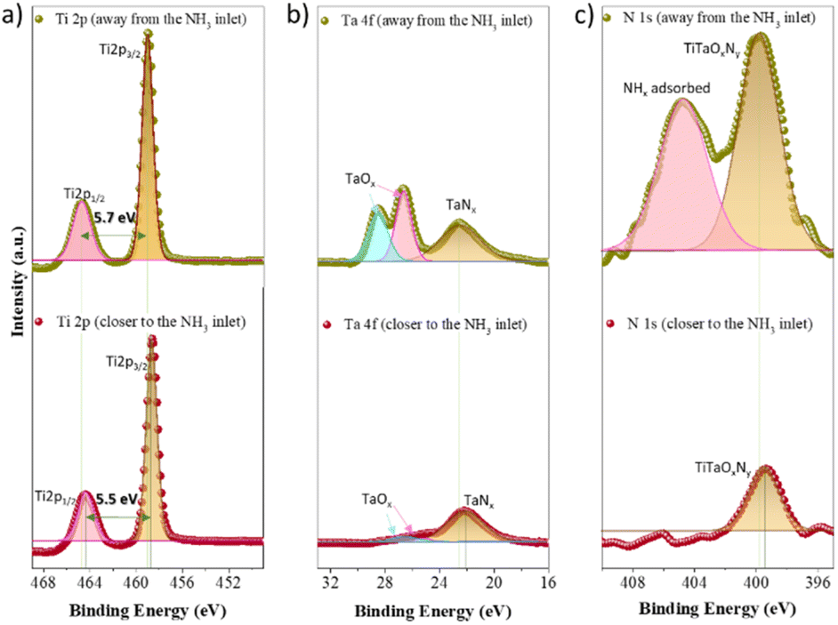 | ||
| Fig. 5 High-resolution XPS spectra of FTO|TTO substrates located at the extremities of the holder (closer to the NH3 inlet and away from the NH3 inlet) during annealing in the oven: (a) Ti 2p region; (b) Ta 4f region; and (c) N 1s region. | ||
Fig. 6 shows the XRD spectra obtained for the as-prepared Ta3N5 photoelectrodes. Ta3N5 is known to crystallize in an orthorhombic structure, characteristic of tantalum in the Ta5+ oxidation state, an oxidation state corresponding to the Ta present in Ta3N5.54 The orthorhombic structure evidenced the total conversion of Ta2O5 to Ta3N5,55 as was observed in all the prepared photoelectrodes, with the intensity of the obtained peaks only varying with the preparation conditions. The characteristics of this phase could be observed with particular emphasis on the (020), (110), (112), (023), (130), (113), and (042) planes with orientations of 17.3°, 24.5°, 30.1°, 31.5°, 35.0°, 36.0°, and 39.4°, respectively.55 The preferential orientation was on the plane (020), which did not present significant differences among the prepared samples. The crystallites' size was determined by Scherrer's equation, and it was found to slightly increase with thicker layers and higher temperature (37.61 nm for the 425-7 sample, 37.72 nm for the 450-5 sample, 42.24 nm for the 450-7 sample, and 42.66 nm for the 475-5 sample). The improved crystallinity should translate into better PEC performances, especially for samples prepared at higher temperatures. However, there were no significant improvements among the best-performing samples, although the samples prepared at lower temperatures presented better power conversion efficiencies. This observation could support the argument that the small differences in the behaviour of the J–E curves plotted in Fig. 4 were not just determined by the characteristics of the Ta3N5 film.
 | ||
| Fig. 6 XRD spectra of the best-performing photoelectrodes under the conditions selected, measured over Ta3N5 film. | ||
To better understand this observation, electrochemical impedance spectroscopy (EIS) was conducted using different Ta3N5 photoelectrodes prepared under different conditions. The EIS measurements were performed in a three-electrode configuration, under 1 sun simulated illumination conditions. The Nyquist plots and the electrical circuit analogue used to fit the impedance data obtained are shown in Fig. 7b. The equivalent circuit proposed consisted of a series resistance (Rseries) and two resistor–capacitor (RC) elements in parallel, assigned to the bulk processes, namely the bulk capacitance, Cbulk, in parallel with its respective resistance, Rbulk, and to the charge-transfer resistance at the semiconductor/electrolyte interface, RCT,int, together with its capacitance, Cint. The fast electronic processes, occurring in the high-frequency range (100 Hz to 1 kHz), were assigned to the events occurring in the semiconductor bulk, since its electronic processes are generally faster than the charge-transfer processes or diffusion of ions in solution.
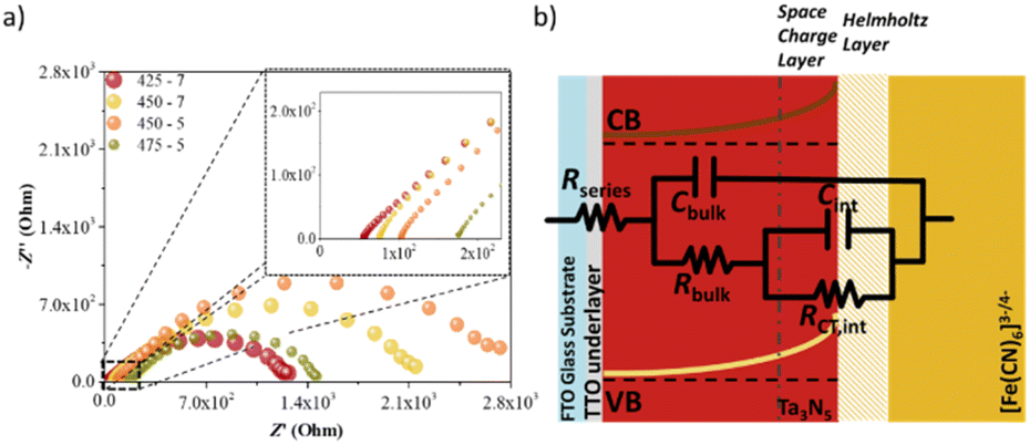 | ||
| Fig. 7 (a) Nyquist plots obtained under 1 sun simulated illumination and when applying a potential of 1.1 VRHE for the Ta3N5 samples prepared under different conditions: 425 °C, 7 min (425-7); 450 °C, 7 min (450-7); 450 °C, 5 min (450-5); and 475 °C, 5 min (475-5), using 0.1 M K4Fe(CN)6 in 1 M KOH as the electrolyte solution; (b) electrical circuit analogue used to fit the impedance data under light conditions (based on ref. 36). | ||
The inset of Fig. 7a shows there were clear differences in the initial Rseries values (high frequencies), with the values being three times higher for the samples prepared at 475 °C compared to the samples annealed at 425 °C. Since Rseries was related to the FTO|TTO layers' resistance, ionic conductivity, and electric contacts,56 this observation suggests that higher annealing temperatures under an ammonia atmosphere were detrimental to the conduction properties of the substrate, thus increasing the ohmic contact resistance between the semiconductor and FTO layers, as previously mentioned. A different trend was observed for the overall resistance (Rtotal = Rseries + Rbulk + RCT,int), and the charge-transfer resistance of the PEC system (Rbulk); see Fig. 8a and b, respectively. The sample 425-7 presented the smallest Rtotal values at all the potentials studied, as was also evident for the lower potentials (until 1.0 VRHE), suggesting that the charge carriers generated in the bulk were more efficiently collected, both by the conductive FTO|TTO substrate (electrons) and as transported by the semiconductor/electrolyte interface (holes). A large charge accumulation at low potentials (until 0.80 VRHE) – characterized by high Cbulk values – was observed, especially for samples 475-5, 450-7 and 450-5; see Fig. S7.† Conversely, the capacitance related to the semiconductor/electrolyte interface, Cint, displayed a different behaviour, showing a maximum peak closer to 0.70 VRHE for the 425-7, 450-7 and 450-5 samples but closer to 0.80 VRHE for sample 475-5, which was coincident with the minimum Rbulk and RCT,int; see Fig. 8 b–d. This indicates that, at these potentials, the accumulated charges tended to be transferred from the semiconductor interface to the electrolyte.
 | ||
| Fig. 8 Impedance parameters obtained from fitting the EIS data under illumination for the best-performing Ta3N5 photoelectrodes [425 °C, 7 min (425-7); 450 °C, 7 min (450-7); 450 °C, 5 min (450-5); and 475 °C, 5 min (475-5)], using 0.1 M K4Fe(CN)6 in 1 M KOH as the electrolyte solution as a function of the applied potential: (a) total resistance, RTotal; (b) bulk resistance, Rbulk; (c) charge-transfer resistance at the semiconductor/electrolyte interface, RCT,int; (d) charge-transfer capacitance at the semiconductor/electrolyte interface, Cint. | ||
Assuming the model proposed by Peter et al.,57 a relationship could be established between the bulk electron-trapping rate constant (kbulk), electron density (n), charge transfer (kCT), electron–hole recombination (krec) with the resistance parameters determined by EIS (Rbulk and RCT,int), and the probability of electron-trap occupation at a given trap energy and applied potential E, (γ(E)) as defined by eqn (5):
 | (5) |
Fig. 9a and b present plots of the parameters kCT and krec as a function of the applied potential, respectively. The shape of the kCT plot was similar to that of Cint, i.e. the maximum peaks were observed at the same potentials for all the studied samples. Alternatively, the smaller peaks for krec were coincident with the potentials when the kCT values were the highest; see Fig. 9b; this corresponded to the onset potential in the J–E curve when charge transfer started from the semiconductor to the electrolyte. In general, samples 450-7 and 450-5 performed worst in terms of charge-accumulation and -transfer at the interface, showing higher rate constants compared to samples 425-7 and 475-5. However, at 0.60 VRHE, the krec and kCT values showed the same order (ca. 1 s−1) for the samples 450-7 and 475-5, which confirmed the competition between the charge-transfer and -recombination phenomena. For the best-performing Ta3N5 photoelectrode (the sample 425-7), kCT was almost three orders of magnitude higher than krec at this lowest applied potential. It was only at high potentials that the sample 475-5 seemed to be almost indistinguishable from the sample 425-7, as was also evident from the J–E curves.
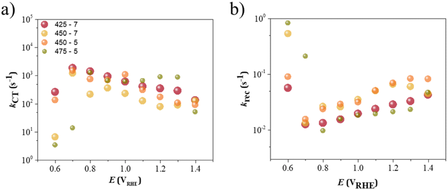 | ||
| Fig. 9 Variation of the rate constants with the applied potentials for (a) charge transfer, and (b) electron–hole recombination, for the Ta3N5 photoelectrodes prepared at 425 °C, 7 min (425-7); 450 °C, 7 min (450-7); 450 °C, 5 min (450-5); and 475 °C, 5 min (475-5), using 0.1 M K4Fe(CN)6 in 1 M KOH as the electrolyte solution. | ||
Proof-of-concept in a lab-scale SRFC using a PEC-PV arrangement
A proof-of-concept SRFC was demonstrated based on the best-performing Ta3N5 photoanode, covered with a commercial ferric passivation overlayer combined with a Co3O4 co-catalyst. These overlayers acted as protective barriers, preventing oxidation and degradation of the photoanode during operation. The UniFlow cell, designed at UPorto58 and displaying a nearly-zero-gap back-to-back configuration, was assembled using the optimized Ta3N5 as the photoanode immersed in 0.1 M K4Fe(CN)6 in 1 M KOH solution, and carbon felt as a counter electrode in contact with 0.05 M 2,7-AQDS in 1 M KOH. Both compartments of the cell were separated by a Nafion 117 membrane, which acted as a proton exchange membrane, allowing selective ion transport while preventing cross-contamination of the electrolytes. The ferrocyanide-2,7-AQDS redox species provided a standard cell potential of ca. 0.74 V, as reported elsewhere.59 However, an additional bias potential was required to photocharge these redox pairs, since the photopotential of the best-performing Ta3N5 sample was only ca. 0.60 V. A PEC-PV arrangement60 was then assembled, pairing a high-potential perovskite solar cell (PSC) in series with the Ta3N5 photoanode; for which a final photopotential of ca. 1.22 V was obtained. Due to the design of the UniFlow SRFC device and the use of coloured electrolyte solutions, a tandem approach was not feasible. Instead, the photoelectrode and the PSC were positioned side by side, as illustrated in Fig. 10a. The J–E curves of the individual photoelectrode and the PSC, as well as the PEC-PV configuration, are presented in the ESI (Fig. S8†).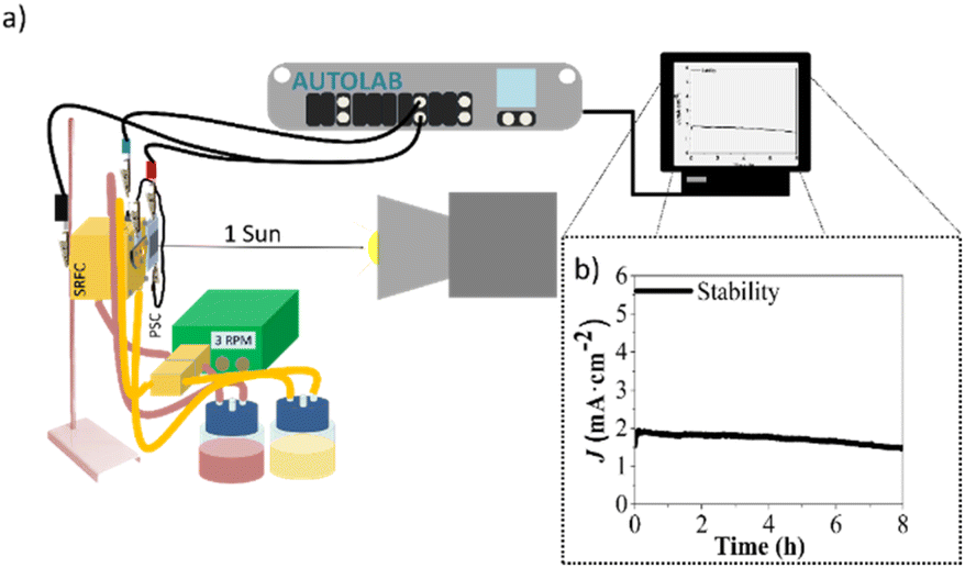 | ||
| Fig. 10 Proof-of-concept of a lab-scale SRFC: (a) scheme of the SRFC with the Ta3N5 photoelectrode in a backside illumination configuration connected to a PSC, immersed in 0.1 M K4Fe(CN)6 in 1 M KOH and using carbon felt as a counter electrode in contact with 0.05 M 2,7-AQDS in 1 M KOH, with both compartments of the cell separated by a Nafion 117 membrane; (b) stability period of the Ta3N5 photoelectrode under 1 sun simulated illumination and applying 0 V. | ||
A stability test was conducted for the Ta3N5-based SRFC by applying an unbiased constant potential of 0 V for over 100 h. Fig. 10b demonstrates the system's stability during the initial period of 8 h, corresponding to a stable photocurrent density of ca. 1.73 mA cm−2 (photocurrent-density loss of <10%). The average photocurrent density recorded over the entire period was ca. 0.56 mA cm−2, which, while not yet suitable for industrial applications, surpasses the stabilities previously reported for this type of photoelectrode. The different effect of the protective layers seemed to disappear after the aging test, although the Ta3N5 film became more compact, as could be seen by the SEM images obtained before and after the stability test; see Fig. S9.†
Conclusions
Semi-transparent Ta3N5 photoelectrodes were prepared over an FTO glass substrate coated with a thin underlayer of TTO. The synthesis conditions, namely the duration of the electrophoretic deposition and the annealing temperature, were systematically optimized. The synthesis conditions for the best-performing photoelectrode (sample 425-7) were 30 nm thick TTO underlayer, 7 min of Ta3N5 electrophoretic deposition, and an annealing temperature of 425 °C. Here, a maximum photocurrent density of ca. 4.0 mA cm−2 was obtained at 1.3 VRHE. This sample also demonstrated a maximum power density of ca. 1.1 mW cm−2 at ca. 1.0 VRHE, which was 21% higher than that obtained for the sample 450-7 (annealed at 450 °C). A new figure-of-merit was proposed, i.e., the power density curves, which balances the photopotential and photocurrent density in the same parameter. The obtained performance was assigned to the reduction of the charge-transfer resistance and recombination rate constant, as observed by the EIS analysis. To the best of our knowledge, this is the best Ta3N5 photoelectrode prepared without the addition of dopants or co-catalysts.The study also allowed greater understanding of the role of the TTO underlayer and concluded that the annealing step directly influences the substrate properties, even at temperatures as low as 450 °C, particularly reducing the photopotential window. These modifications were assigned to reducing the effect of the ammonia atmosphere, as well as the position of the samples in the oven, namely closer or further away from the NH3 feed stream, as revealed by the XPS and XRD analyses. When increasing the annealing temperature, an onset potential shift of the J–E curve under light for more cathodic potentials and a decrease in the fill factor were observed. The series resistance of the 475-5 photoelectrode (prepared by 5 min of Ta3N5 EPD and annealing at 475 °C) was the highest obtained.
Unbiased photocharging of a ferrocyanide/AQDS in a lab-scale SRFC was demonstrated using a PEC-PV arrangement, based on the optimized Ta3N5 photoelectrode and a perovskite solar cell in series. The performance of this system was evaluated over 100 h, and an average photocurrent of ca. 0.56 mA cm−2 was measured when applying 0 V.
Data availability
The data related to the article cannot be made available due to legal or ethical confidentiality requirements.Conflicts of interest
The authors declare that they have no known competing financial interests or personal relationships that could have appeared to influence the work reported in this article.Acknowledgements
Filipe Moisés M. Francisco and Paula Dias are grateful to FCT for the funding (references: SFRH/BD/146338/2019 and CEECIND/02862/2018, respectively). This work is financially supported by national funds through the FCT/MCTES (PIDDAC), under the project ASAPFuels - PTDC/EQU-EQU/4225/2021 (DOI: 10.54499/PTDC/EQU-EQU/4225/2021), and by LEPABE, UIDB/00511/2020 (DOI: 10.54499/UIDB/00511/2020) and UIDP/00511/2020 (DOI: 10.54499/UIDP/00511/2020) and ALiCE, LA/P/0045/2020 (DOI: 10.54499/LA/P/0045/2020). The authors also are very thankful to Ana Mafalda Pereira for the determination of TiO2 and TTO work function parameters using the Kelvin probe; Jeffrey Capitão and Dzmitry Ivanou for the fruitful discussions about challenging depositions of TTO by ALD; Marta Pereira for providing the perovskite solar cell; and André Gonçalves for all the support with the nitrification setup.Notes and references
- Y. He, Z. Deng, J. Chen, W. Li, J. Zhou, F. Xiang and X. Hu, J. Energy Chem., 2024, 98, 1–11 CrossRef.
- ClimateWatchData, Historical GHG Emissions, https://www.climatewatchdata.org/ghg-emissions?breakBy=sector%26chartType=percentage%26end_year=2018%26start_year=1990, accessed 31 August 2024 Search PubMed.
- T. da Silva Lopes, P. Dias, R. Monteiro, A. Vilanova, D. Ivanou and A. Mendes, Adv. Energy Mater., 2021, 12, 2102893 CrossRef.
- L. Andrade, T. Lopes, H. A. Ribeiro and A. Mendes, Int. J. Hydrogen Energy, 2011, 36, 175–188 CAS.
- A. Z. Weber, M. M. Mench, J. P. Meyers, P. N. Ross, J. T. Gostick and Q. Liu, J. Appl. Electrochem., 2011, 41, 1137–1164 CAS.
- Y. Sun, Z. Li, B. Sun, Y. Mao, B. Huang and H. Cheng, Mater. Chem. Front., 2024, 8, 1300–1333 CAS.
- F. Francisco, P. Dias, D. Ivanou, F. Santos, J. Azevedo and A. Mendes, ChemNanoMat, 2019, 5, 911–920 CAS.
- Y. He, R. Chen, W. Fa, B. Zhang and D. Wang, J. Chem. Phys., 2019, 151, 130902 Search PubMed.
- J. Liu, W. Luo, K. Zhu, X. Wen, F. Xiu, J. Yuan, Z. Zou and W. Huang, RSC Adv., 2017, 7, 30650–30656 CAS.
- A. Vilanova, P. Dias, T. Lopes and A. Mendes, Chem. Soc. Rev., 2024, 53, 2388–2434 CAS.
- G. Liu, S. Ye, P. Yan, F. Xiong, P. Fu, Z. Wang, Z. Chen, J. Shi and C. Li, Energy Environ. Sci., 2016, 9, 1327–1334 CAS.
- Q. Cheng, W. Fan, Y. He, P. Ma, S. Vanka, S. Fan, Z. Mi and D. Wang, Adv. Mater., 2017, 29, 1700312 Search PubMed.
- M. Higashi, K. Domen and R. Abe, Energy Environ. Sci., 2011, 4, 4138–4147 CAS.
- L. Pei, Z. Xu, Z. Shi, H. Zhu, S. Yan and Z. Zou, J. Mater. Chem. A, 2017, 5, 20439–20447 CAS.
- M. Liao, J. Feng, W. Luo, Z. Wang, J. Zhang, Z. Li, T. Yu and Z. Zou, Adv. Funct. Mater., 2012, 22, 3066–3074 CAS.
- Z. Wang, Y. Qi, C. Ding, D. Fan, G. Liu, Y. Zhao and C. Li, Chem. Sci., 2016, 7, 4391–4399 CAS.
- H. Hajibabaei, D. J. Little, A. Pandey, D. Wang, Z. Mi and T. W. Hamann, ACS Appl. Mater. Interfaces, 2019, 11, 15457–15466 CAS.
- H. Hajibabaei, O. Zandi and T. W. Hamann, Chem. Sci., 2016, 7, 6760–6767 CAS.
- W. Lei, Y. Yu, H. Zhang, Q. Jia and S. Zhang, Mater. Today, 2022, 52, 133–160 CrossRef CAS.
- M. Li, W. Luo, L. Yang, X. Zhao and Z. Zou, Aust. J. Chem., 2016, 69, 631–638 CrossRef CAS.
- L. Bi, X. Liang, W. Zhang, Z. Wu, J. Zhan, T. Xie, L. Zhang, W. Xu, J. Jiang and M. Wu, Colloids Surf., A, 2024, 683, 133103 CrossRef CAS.
- Y. Sim, J. John, S. Surendran, B. Moon and U. Sim, Appl. Sci., 2018, 9, 16 CrossRef.
- H.-H. Wang, Q. Chen, H. Zhou, L. Song, Z. S. Louis, N. D. Marco, Y. Fang, P. Sun, T.-B. Song, H. Chen and Y. Yang, J. Mater. Chem. A, 2015, 3, 9108–9115 RSC.
- J. Chung, S. S. Shin, K. Hwang, G. Kim, K. W. Kim, D. S. Lee, W. Kim, B. S. Ma, Y.-K. Kim, T.-S. Kim and J. Seo, Energy Environ. Sci., 2020, 13, 4854–4861 CAS.
- D. Eisenberg, H. S. Ahn and A. J. Bard, J. Am. Chem. Soc., 2014, 136, 14011–14014 CAS.
- H. Mo, D. Wang, Q. Chen, W. Guo, S. Maniyarasu, A. G. Thomas, R. J. Curry, L. Li and Z. Liu, ACS Appl. Mater. Interfaces, 2022, 14, 15141–15153 CAS.
- J. Li, J. Bai, X. Niu, X. Li, S. Chen, J. Wang and B. Zhou, Int. J. Hydrogen Energy, 2018, 43, 18202–18210 CAS.
- M. Rudolph, I. Vickridge, E. Foy, J. Alvarez, J. P. Kleider, D. Stanescu, H. Magnan, N. Herlin-Boime, B. Bouchet-Fabre, T. Minea and M. C. Hugon, Thin Solid Films, 2019, 685, 204–209 CAS.
- M. S. Yu, S. C. Jesudass, S. Surendran, J. Y. Kim, U. Sim and M. K. Han, ACS Appl. Mater. Interfaces, 2022, 14, 31889–31899 CAS.
- A. F. T. Gonçalves, F. S. M. Sinfrônio, A. S. de Menezes and A. Mendes, Mater. Today Commun., 2022, 32, 104122 Search PubMed.
- G. Liu, J. Shi, F. Zhang, Z. Chen, J. Han, C. Ding, S. Chen, Z. Wang, H. Han and C. Li, Angew. Chem., Int. Ed., 2014, 53, 7295–7299 CrossRef CAS PubMed.
- G. Beamson and D. R. Briggs, In High Resolution XPS of Organic Polymers: The Scienta ESCA300 Database, Wiley, 1992 Search PubMed.
- C. Mahata, H. Algadi, M. Ismail, D. Kwon and S. Kim, J. Mater. Sci. Technol., 2021, 95, 203–212 CAS.
- J. F. Moulder, J. Chastain and R. C. King, In Handbook of X-Ray Photoelectron Spectroscopy: A Reference Book of Standard Spectra for Identification and Interpretation of XPS Data, Physical Electronics Division, Perkin-Elmer Corp, Eden Prairie, Minn, 1995 Search PubMed.
- V. D. Mote, Y. Purushotham and B. N. Dole, Journal of Theoretical and Applied Physics, 2012, 6, 6 Search PubMed.
- P. Dias, L. Andrade and A. Mendes, Nano Energy, 2017, 38, 218–231 CAS.
- A. S. Wochnik, M. Handloser, D. Durach, A. Hartschuh and C. Scheu, ACS Appl. Mater. Interfaces, 2013, 5, 5696–5699 CAS.
- M. J. Alam and D. C. Cameron, J. Sol-Gel Sci. Technol., 2002, 25, 137–145 CAS.
- C.-H. Lu and W.-H. Wu, Mater. Sci. Eng., B, 2004, 113, 42–45 Search PubMed.
- M. Cesaria, L. Scrimieri, A. Torrisi, G. Quarta, A. Serra, D. Manno, A. P. Caricato, M. Martino, L. Calcagnile and L. Velardi, Vacuum, 2022, 202, 111150 CAS.
- H. Dotan, N. Mathews, T. Hisatomi, M. Gratzel and A. Rothschild, J. Phys. Chem. Lett., 2014, 5, 3330–3334 CAS.
- B. Bharti, S. Kumar, H. N. Lee and R. Kumar, Sci. Rep., 2016, 6, 32355 CAS.
- R. S. Devan, V. P. Thakare, V. V. Antad, P. R. Chikate, R. T. Khare, M. A. More, R. S. Dhayal, S. I. Patil, Y. R. Ma and L. Schmidt-Mende, ACS Omega, 2017, 2, 2925–2934 CAS.
- W. D. Song, J. F. Ying, W. He, V. Y. Q. Zhuo, R. Ji, H. Q. Xie, S. K. Ng, S. L. G. Ng and Y. Jiang, Appl. Phys. Lett., 2015, 106, 031602 CrossRef.
- Y. Wang, Y. Yan, C. Wang, Y. Chen, J. Li, J. Zhao and C. S. Hwang, Appl. Phys. Lett., 2018, 113, 072902 CrossRef.
- A. K. Chakraborty, S. Ganguli and M. A. Sabur, J. Water Proc. Eng., 2023, 55, 104183 Search PubMed.
- Y. Chen, Y. Yan, J. Wu, C. Wang, J. Y. Lin, J. S. Zhao and C. S. Hwang, ACS Appl. Mater. Interfaces, 2020, 12, 10681–10688 CrossRef CAS PubMed.
- M. Pisarek, M. Krawczyk, M. Holdynski and W. Lisowski, ACS Omega, 2020, 5, 8647–8658 CrossRef CAS PubMed.
- S. Liu, J. Yu and W. Wang, Phys. Chem. Chem. Phys., 2010, 12, 12308–12315 RSC.
- P. Hess, Nanoscale Horiz., 2021, 6, 856–892 RSC.
- R. Asahi, T. Morikawa, T. Ohwaki, K. Aoki and Y. Taga, Science, 2001, 293, 269–271 CrossRef CAS PubMed.
- R. Beranek, B. Neumann, S. Sakthivel, M. Janczarek, T. Dittrich, H. Tributsch and H. Kisch, Chem. Phys., 2007, 339, 11–19 CAS.
- D. Pjević, T. Savić, S. Petrović, D. Peruško, M. Čomor and J. Kovač, ECS J. Solid State Sci. Technol., 2021, 10, 053002 Search PubMed.
- E. Nurlaela, M. Harb, S. del Gobbo, M. Vashishta and K. Takanabe, J. Solid State Chem., 2015, 229, 219–227 CAS.
- J. Eichhorn, S. P. Lechner, C. M. Jiang, G. Folchi Heunecke, F. Munnik and I. D. Sharp, J. Mater. Chem. A, 2021, 9, 20653–20663 CAS.
- T. Lopes, L. Andrade, F. Le Formal, M. Gratzel, K. Sivula and A. Mendes, Phys. Chem. Chem. Phys., 2014, 16, 16515–16523 RSC.
- K. G. Upul Wijayantha, S. Saremi-Yarahmadi and L. M. Peter, Phys. Chem. Chem. Phys., 2011, 13, 5264–5270 CAS.
- T. da Silva Lopes, P. Dias and A. Mendes, 10th Solar Fuels Network Symposium, Newcastle, United Kingdom (Oral Communication), personal communication, 2022 Search PubMed.
- K. Wedege, J. Azevedo, A. Khataee, A. Bentien and A. Mendes, Angew. Chem., Int. Ed., 2016, 55, 7142–7147 CAS.
- H. He, Q. Zhang, Z. Wang, S. Pan, Y. Zhao and X. Zhang, Adv. Energy Mater., 2024, 14, 2303713 CAS.
Footnote |
| † Electronic supplementary information (ESI) available. See DOI: https://doi.org/10.1039/d4ta08136f |
| This journal is © The Royal Society of Chemistry 2025 |