Achieved excellent energy storage performance under moderate electric field in BaTiO3-modified Bi0.5Na0.5TiO3-based lead-free ceramics via multiple synergistic design†
Xiangluo
Miao
a,
Run
Jing
a,
Zhenhui
Zhang
a,
Xiangbin
Zhang
a,
Shibang
Zhang
a,
Pengfei
Li
a,
Changan
Wang
 *b,
Chung Ming
Leung
c,
Xingsen
Gao
 a and
Min
Zeng
 *a
*a
aGuangdong Provincial Key Laboratory of Quantum Engineering and Quantum Materials, and Institute for Advanced Materials, South China Academy of Advanced Optoelectronics, South China Normal University, Guangzhou 510006, China. E-mail: zengmin@scnu.edu.cn
bJinhua Advanced Research Institute, Jinhua, 321004, China. E-mail: wangchangan@gdisit.com
cSchool of Mechanical Engineering and Automation, Harbin Institute of Technology, Shenzhen, China
First published on 31st October 2024
Abstract
Dielectric capacitors show great potential for use in pulse power devices due to their high power density. However, achieving ultrahigh recoverable energy density (Wrec) and efficiency (η) remains a challenge, limiting their applications. To address this, Na0.5Bi0.5TiO3–BaTiO3 (NBT-BT) ceramics were optimized for energy storage devices operating at a relatively low electric field (E). This study introduces a synergistic optimization strategy by incorporating Ca(Hf0.7Zr0.3)O3 (CHZ) into 0.93NBT–0.07BT (BNBT) ceramics. The addition of CHZ, in concentrations ranging from x = 0.00 to 0.18, significantly enhances the differences between saturation and remnant polarization from 15.6 μC cm−2 to 42.5 μC cm−2, while reducing the grain size from 2.44 μm to 620 nm. An optimal Wrec of ∼5.09 J cm−3 with η of ∼77% was achieved in BNBT–0.14CHZ ceramics at a moderate electric field (283 kV cm−1). Moreover, the energy storage density and efficiency exhibited good frequency stability (10–1000 Hz), temperature stability (25–150 °C) and fatigue resistance (1–104 cycles). A fast discharge time (∼72 ns) was concurrently realized at x = 0.14 ceramics. These results suggest that the eco-friendly BNBT–0.14CHZ ceramic is a promising candidate for application in dielectric energy storage capacitors under moderate electric field.
1. Introduction
Dielectric ceramic capacitors, as potential high-power energy storage devices, have attracted increasing attention due to their advantages of high power density, fast charging and discharging speed, good stability, and low cost.1 However, the low energy storage density remains a major bottleneck that needs to be addressed, significantly limiting their applications. Generally, the energy storage performance (ESP) of dielectric capacitors is determined by three parameters:2 total energy storage density (Wtol), recoverable energy storage density (Wrec) and energy storage efficiency (η). These parameters are typically derived from the hysteresis loop of the polarized-electric field and are defined by the following equations:3 ,
,  and
and  where Pm, Pr and E denote maximum polarization value, remnant polarization value and the applied electric field, respectively. A large polarization discrepancy ΔP (ΔP = Pm − Pr) and a high breakdown strength (BDS) are beneficial for achieving high ESP. Among all reported dielectric systems, relaxor ferroelectrics (RFE) have shown great promise as energy storage materials due to their relatively large Pm, decent electric field, and narrow hysteresis loops. For instance, Chen et al. reported a great Wrec of ∼11.2 J cm−3 with a ΔP of ∼49 μC cm−2 at 400 kV cm−1 in (Pb0.94Sm0.04)(Zr0.6Sn0.4)O3 ceramic.4 Zhou et al. revealed a Wrec of ∼3.74 J cm−3 with a ΔP of ∼35.5 μC cm−2 under 273 kV cm−1 at a BaTiO3-based ceramic.5 Despite these promising results, the inherent inversion correlation between polarization and BDS in relaxor ferroelectrics remains a limiting factor for achieving further improvements in ESP. To address this challenge, novel structure designs such as core–shell structures and multi-layered ceramics have been widely explored. For example, Huang et al. achieved an excellent Wrec of ∼5.92 J cm−3 and a η of ∼81.7% at 552.3 kV cm−1 in the core–shell Ba0.55Sr0.39Zn0.06TiO3–BiMg2/3Nb1/3O3 ceramics.6 Ma et al. designed 0.65Bi0.5Na0.5TiO3–0.35SrTiO3–0.15La(Mg1/2Zr1/2)O3 multilayered ceramics with an ultrahigh Wrec of ∼13.5 J cm−3 at 1050 kV cm−1.7
Recently, environmentally friendly lead-free RFE ceramics, such as BaTiO3 (BT), Na0.5Bi0.5TiO3 (NBT) and BiFeO3 (BF) have also attracted great attention. For instance, Dai et al. reported a Wrec of ∼3.81 J cm−3 and a η of ∼90.5% at 405 kV cm−1 in Ba0.85Ca0.15Zr0.1Ti0.9O3–0.075BiMg2/3Nb1/3O3 ceramics.8 Luo et al. achieved an extraordinary Wrec of 6.02 J cm−3 and a superior η of 94.5% at 450 kV cm−1 in a new type of lead-free 0.94Bi0.47Na0.47Ba0.06TiO3–0.06CaHfO3–0.45Bi0.2Sr0.7TiO3 relaxor ferroelectric ceramics.9 Zhao et al. also obtained a large Wrec ∼ 6 J cm−3 along with superior η of ∼90% at 520 kV cm−1 by incorporating BaTiO3–Bi(Li1/3Hf2/3)O3 into BiFeO3.10 Although significant progress has been made, the majority of these results are obtained at high electric fields (>500 kV cm−1). However, high E limits the applicability due to environmental concerns and increased losses during long-term operation.11 Therefore, developing new lead-free ceramics with excellent Wrec at relatively low E remains a critical challenge.
It is noted that a high ΔP is a prerequisite for achieving high ESP under a low electric field. Among traditional ferroelectric materials, the lead-free NBT-BT system with a morphotropic phase boundary (MPB) is a promising candidate for energy storage applications due to its good ferroelectricity (Pm > ∼40 μC cm−2)12 and high Curie temperature (>320 °C).13 Unfortunately, high remnant polarization severely limits the energy storage density and efficiency. To address this issue, ion doping and the construction of new solid solutions have been employed. For instance, a high Wrec of ∼4.60 J cm−3 with a η of ∼82% at 260 kV cm−1 was reported in Na0.5Bi0.5TiO3–Sr0.7Bi0.2TiO3–0.04Ag0.9Ca0.05NbO3 ceramic.14 Nie et al. revealed a Wrec of ∼3.14 J cm−3 and a η of ∼71.3% at 250 kV cm−1 for Na0.5Bi0.5TiO3–BaTiO3–BiFeO3–0.15CaTiO3 ceramic.15 Although some progress has been made in NBT-BT-based ceramics, a high ESP with a large Wrec (>5 J cm−3) and large η (>70%) is still hard to obtain at a relatively low electric field (<300 kV cm−1).
To address the challenges and further enhance the ESP of NBT-BT-based ceramics, the primary method involves regulating the compositional disorder of A/B sites. This is achieved by enhancing relaxor behavior, employing nanodomain engineering, and refining grain size, as illustrated in Fig. 1. To design NBT-BT-based ceramics for energy storage devices with high ESP at relatively low electric fields, a multiscale optimization strategy is proposed by introducing CHZ into BNBT ceramics. The rationale for selecting CHZ as the chemical modifier is as follows: (1) Hf elements, known for their wide bandgap and superior quality, contribute effectively to grain refinement. For example, Luo et al. introduced Hf4+ into Bi0.47Na0.47Ba0.06TiO3, achieving a fine grain size of ∼0.59 μm.13 (2) The introduction of weakly polar ions Ca2+ and Zr4+ induces local random field effects, disrupting the long-range ferroelectric (FE) sequence and generating polar nanoregions (PNRs), thereby improving ESP. Acosta et al. incorporated CaZrO3 into Bi0.5Na0.5TiO3–BaTiO3, which contributed to non-uniform domain structures, further enhancing ESP.16 By utilizing this synergistic optimization strategy, a high ESP at moderate electric fields can be achieved.
 | ||
| Fig. 1 Schematic diagram of the strategy for achieving excellent energy storage properties under a relatively low electric field via synergistic optimization design. | ||
Motivated by this approach, (Bi0.5Na0.5)0.93Ba0.07TiO3–xCa(Hf0.7Zr0.3)O3 (x = 0.00, 0.10, 0.12, 0.14, 0.16, and 0.18) lead-free ceramics were synthesized using a conventional solid-state sintering method. Remarkably, a giant Wrec of ∼5.09 J cm−3 and a η of ∼77% were obtained at a moderate of ∼283 kV cm−1 for BNBT–0.14CHZ ceramics, along with an ultrahigh ΔP of ∼42.5 μC cm−2. Furthermore, the optimal ceramics have good frequency stability (10–1000 Hz), good temperature stability (25–150 °C), superior fatigue resistance (1–104 cycles), and a rapid discharge time (∼72 ns). The mechanism for improving ESP will be explored.
2. Experimental methods
The (Bi0.5Na0.5)0.93Ba0.07TiO3–xCa(Hf0.7Zr0.3)O3 (x = 0.00, 0.10, 0.12, 0.14, 0.16, and 0.18) lead-free ceramics were synthesized via a conventional solid-state sintering method. The raw materials, including Bi2O3 (99.99%), Na2CO3 (99.8%), BaCO3 (99.95%), TiO2 (99.99%), CaCO3 (99.99%), HfO2 (99.9%), and ZrO2 (99.99%) were weighed according to their stoichiometric formula and ball-milled for 24 h in ethanol. The collected powders were pre-sintered at 800 °C for 2 h, mixed with 5% PVA, and then pressed into discs with a diameter of approximately 13 mm and a thickness of about 1 mm at a pressure of 10 MPa. Prior to sintering, the samples were heated to 600 °C and held for 120 minutes to discharge the PVA. Finally, all samples were sintered at 1100–1200 °C for 3 h.X-ray diffraction (XRD) using a PANalytical X'Pert PRO diffractometer was employed to investigate the crystal structure. Raman spectroscopy was conducted using a Raman scattering spectrometer (inVia, RENISHAW, UK). Microstructure analysis was performed using a scanning electron microscope (SEM, ZEISS Ultra 500, Germany). The polished discs were thermally etched at 950 °C for 10 minutes before SEM examination. Dielectric behavior was characterized using an LCR meter (E4980A, Agilent). Ferroelectric properties were measured by recording P–E loops with a ferroelectric analyzer (Radiant Technology). Ultraviolet-visible absorbance spectra was characterized by a UV-vis spectrophotometer (UV2600, Shimadzu, Kyoto, Japan), and the domain morphologies were observed with a transmission electron microscope (TEM, JEM-2100HR, JEOL, Japan).
3. Results and discussion
The XRD patterns of the BNBT–xCHZ (x = 0.00, 0.10, 0.12, 0.14, 0.16, and 0.18) ceramics are presented in Fig. 2(a). Each sample shows a typical cubic perovskite structure without any impure peak, indicating that CHZ is well incorporated into the BNBT matrix. A detailed analysis of the (200) diffraction peak, as shown in Fig. 2(b), reveals a gradual shift towards a lower angle with increasing CHZ doping content (x), suggesting lattice expansion. This shift is attributed to the substitution of Ti4+ (CN6, 0.605 Å) at the B-site by Hf4+ (CN6, 0.71 Å) and Zr4+ (CN6, 0.84 Å), which have larger ionic radii. Raman spectra was used to measure their vibration modes and local structure. As exhibited in Fig. 2(c), the active mode below 200−1 related to the A-site vibration, remains almost unchanged across all CHZ doping levels, suggesting that the high polarization can be primarily maintained through Bi ion activity.17,18 In contrast, the Raman active mode between 500–600 cm−1 weakens and diffuses toward higher wave numbers as CHZ content increases. This phenomenon is due to the more disordered lattice structures induced by CHZ, which contribute to the improvement of relaxor behavior. | ||
| Fig. 2 (a) XRD patterns of BNBT–xCHZ ceramics and (b) The enlarged (200) peaks. (c) Room-temperature Raman spectra for BNBT–xCHZ ceramics. | ||
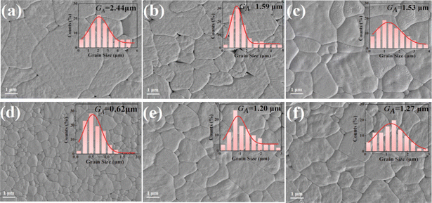
Fig. 3(a)–(f) display the SEM micro-images of the thermally-etched BNBT–xCHZ ceramics. All ceramics exhibit a dense microstructure with low porosity and well-defined grain boundaries. The corresponding insets in Fig. 3(a)–(f) exhibit their grain size distributions. Upon increasing x, the average grain size (GA) first gradually decreases and then slightly increases. The reduced GA can be attributed to the doping of CHZ, in which the larger ionic radius and the heavier atomic mass could hinder the ion-diffusion rates in sintering, retarding grain growth. When x > 0.14, a slight increase in GA can be seen, possibly indicating that excessive doping leads to crystal lattice defects and abnormal grain growth.19 The smallest GA of ∼0.62 μm is obtained at x = 0.14 ceramics. Based on the relationship:  20 it is expected that smaller grains will improve the BDS.
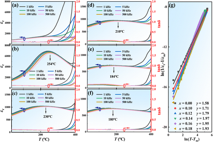
Fig. 4(a)–(f) present the dielectric properties of BNBT–xCHZ ceramics at different temperatures (T). For the ceramics with x = 0.00, the dielectric peak exists above 400 °C making it undetectable due to the experimental range (T ∈ (−50 °C, 400 °C)). Upon the introduction of CHZ, a relaxor-like peak, exhibiting frequency dependence, emerges, signifying a transition from ferroelectric to relaxor characteristics.18 As the CHZ content increases further, the relaxor dielectric peak becomes gradually suppressed, broadened, and shifts towards lower T, indicating enhanced relaxor behavior.21 To accurately explore the relaxation behavior of ceramics, the modified Curie–Weiss method22 was employed to evaluate the relaxation degree (γ) by the equation: 1/ε − 1/εm = (T − Tm)γ/C, at T > Tm, where εm and Tm is the maximum dielectric constant and the corresponding T, respectively, and C is the constant. The curves of log(1/ε − 1/εm) and log(T − Tm) at 500 kHz are plotted in Fig. 4(g). The parameter γ is defined between 1 and 2, where 1 corresponds to an ideal ferroelectric and 2 corresponds to an ideal relaxor ferroelectric.20 Compared to pure BNBT (x = 0.00) ceramics (γ = 1.58), the γ value increases almost linearly with CHZ content, further confirming the enhancement of relaxor behavior,19,23 which is consistent with the Raman results shown in Fig. 2(c).
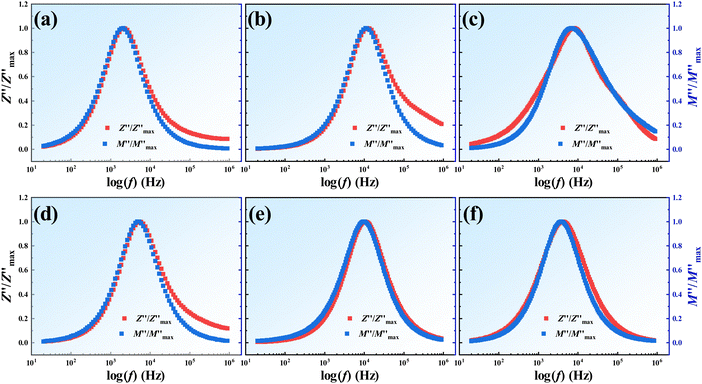
To investigate the influence of grains, grain boundaries, and electrode interfaces on the conductivity behavior, the complex impedance plots (Z′ − Z′′) of BNBT–xCHZ ceramics from 370 °C to 450 °C were measured and signified in Fig. 5(a)–(f). All samples exhibit a single semicircular arc, indicating a single relaxation mechanism caused by the grains of the ceramic, which is classified as a bulk response.21 This is because the grain boundary and electrode responses are not observed within the tested temperature and frequency ranges. For all samples, as the temperature increases, the intercept of the curve on the x-axis decreases, which is attributed to the oxygen vacancies generated at higher temperatures.12 With increasing doping content (x), the impedance initially increases and then decreases, reaching its maximum value in BNBT–0.14CHZ ceramics. This behavior is related to the refinement of grain size, as shown in Fig. 3, while the subsequent decrease with excessive doping is likely due to defects between the grain boundaries.24 Moreover, grains and grain boundaries in ceramics generally correspond to different electroactive regions, each having distinct time constants, characteristic frequencies, and activation energies. The electroactive regions of ceramics are further explored using Z′′ and M′′, measured at 410 °C, as a function of frequency and normalized in Fig. 6(a)–(f).25M* represents electric modulus, which can be expressed in terms of Z* through the following equations: M* = M′ + jM′′ = jωC0Z* = ωC0Z′′ + jωC0Z′. Notably, for all samples, the two curves nearly overlap, suggesting that the electroactive properties of the ceramic grains and grain boundaries are similar, indicating good electrical homogeneity in the ceramics. This homogeneity helps to reduce the likelihood of local electrical breakdown.
 | ||
| Fig. 5 The complex impedance spectra of the BNBT–xCHZ ceramics from 370 °C to 450 °C: (a) x = 0.00, (b) x = 0.10, (c) x = 0.12, (d) x = 0.14, (e) x = 0.16, and (f) x = 0.18. | ||
At 410 °C, Z-view software was used to fit the arcs of complex impedance. The corresponding R-CPE component was selected to match the shape of the curve, as shown in Fig. 7(a) [see Table S2 for the fitted parameters, ESI†]. Moreover, based on the Arrhenius fitting: σ = σ0![[thin space (1/6-em)]](https://www.rsc.org/images/entities/char_2009.gif) exp(Ea/kBT), where σ is conductivity, σ0 is the constant and kB is the Boltzmann constant, the activation energy (Ea) are calculated. This energy reflects the barrier that must be overcome for carrier injection into the dielectric. As shown in Fig. 7(b), the maximum Ea is obtained at BNBT–0.14CHZ ceramics for 1.741 eV. A high Ea also indicates that the ceramic has a strong resistance to electrical breakdown.
exp(Ea/kBT), where σ is conductivity, σ0 is the constant and kB is the Boltzmann constant, the activation energy (Ea) are calculated. This energy reflects the barrier that must be overcome for carrier injection into the dielectric. As shown in Fig. 7(b), the maximum Ea is obtained at BNBT–0.14CHZ ceramics for 1.741 eV. A high Ea also indicates that the ceramic has a strong resistance to electrical breakdown.
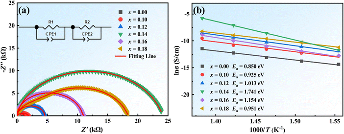 | ||
| Fig. 7 (a) Equivalent model and fitting results of BNBT–xCHZ ceramics at 410 °C and (b) relationship between ln(σ) and 1000/T for BNBT–xCHZ ceramics. | ||
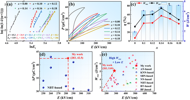
To evaluate the average Eb values of BNBT–xCHZ ceramics, a Weibull distribution analysis was conducted. As shown in Fig. 8(a), the large slope value (β > 14) demonstrated good reliability.20 The average Eb increases steadily from 119 to 286 kV cm−1. This enhancement in Eb is not only related to grain refinement but also to the reduced dielectric loss (see Fig. 4) and leakage current (see Fig. S2, ESI†). Next, the unipolar P–E loops tested at the average Eb and 100 Hz are presented in Fig. 8(b). For the ceramics with x = 0.00, a well-saturated P–E loop with large hysteresis is exhibited, illustrating a typical ferroelectric behavior.26 The maximum polarization Pm is up to ∼58.6 μC cm−2, which is consistent with the reports.21,22 Upon increasing CHZ doping content, the shape of P–E loops become slimmer, indicating the transformation from FE to RFE. Notably, an ultrahigh ΔP of up to ∼42.5 μC cm−2 is achieved in BNBT–0.14CHZ ceramics, which is higher than most reported NBT-based ceramics,13–15,27–31 as summarized in Fig. 8(d). The ultrahigh ΔP value should be owing to the large lattice distortions in the perovskite structure.12 Consider that the ferroelectric polarization in NBT-based ceramics is mainly attributed to the hybridizations between 6p electrons of Bi3+ and 2p electrons of O2− orbitals. In this work, the substitutions of Bi3+ by Na+, Ba2+ and Ca2+ on A-sites, and Ti4+ by Hf4+ and Zr4+ on B-sites could further enhance the lattice distortion. It was also widely reported that doping can enhance the polarization of NBT-based ceramics.11 According to these P–E data, the corresponding Wrec and η can be evaluated, and shown in Fig. 8(c) as a function of doping CHZ content, x. It can be found that an a giant Wrec of ∼5.09 J cm−3 and a η of ∼77% are achieved in BNBT–0.14CHZ. A comparison of Wrec and η between our BNBT–0.14CHZ ceramics and previously reported lead-free dielectric ceramics5,8–10,13,26,27,30–50 is summarized in Fig. 8(e). It can be seen that the achievement of a giant Wrec (>5 J cm−3) usually requires a large E (>400 kV cm−1), while our BNBT–0.14CHZ ceramics receive an excellent Wrec of ∼5.09 J cm−3 at a moderate E of 283 kV cm−1, indicating great potential for applications at moderate electric field.
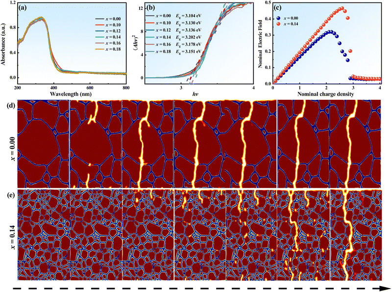
To explore the intrinsic mechanism of the enhanced BDS in BNBT–xCHZ ceramics, their UV spectrophotometer were measured and results are displayed in Fig. 9(a). From Fig. 9(a), the band gap width (Eg) could be calculated by the Tauc equation:13 (hv)2 = A(hv − Eg), where h, A, α, and v are the Planck constant, the constant, the absorption coefficient, and the frequency, respectively. The detailed derivation of Eg is enlarged in Fig. 9(b), and the value of Eg is listed in the insert in Fig. 9(b). It can be seen that Eg gradually increases from 3.104 eV @ x = 0.00 to 3.202 eV @ x = 0.14 ceramics. The increased Eg indicates that it becomes more difficult for electrons in the valence band to transition to the conduction band,9 which contributes significantly to the enhanced BDS and the consequent improvement in ESP. However, excessive doping creates a disproportionate relationship between Eg and Eb, likely due to the appearance of small pores, as shown in Fig. 3(e) and (f).
To further explore the effect of grain size on the BDS, COMSOL Multiphysics Software was used to analyze the breakdown behavior of the BNBT–xCHZ ceramics with x = 0.00 and x = 0.14. The breakdown path diagrams at different moments are shown in Fig. 9(d) and (e), respectively. It is evident that the breakdown path initiates from a point at the top of the intensified field and gradually spreads throughout the ceramic. In contrast, the ceramics with x = 0.14 exhibit a longer breakdown time along the breakdown path at the grain boundary, indicating that CHZ could run as a “strengthened grain boundary” in the ceramic, contributing to the refined grain size and improved Eb. As exhibited in Fig. 9(c), the nominal electric field of BNBT–0.14CHZ ceramic is significantly higher compared to the BNBT–xCHZ ceramic with x = 0.00, demonstrating the substantial enhancement in breakdown strength due to the introduction of CHZ.
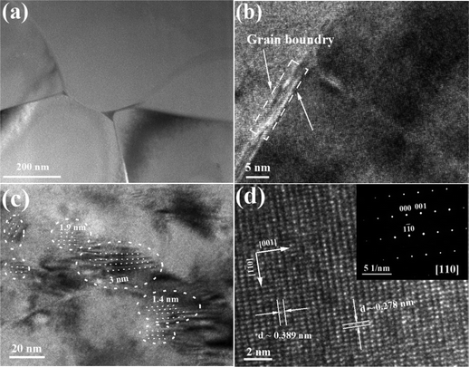
The optimal BNBT–0.14CHZ ceramics were further studied with TEM to investigate the relationship between the ESP and microstructure. The low-resolution TEM in Fig. 10(a) reveals a well-organized grain structure with tightly connected grain boundaries. Fig. 10(b) further confirms the tightly bonded grain boundaries, free of voids. These dense grain boundaries not only inhibit the diffusion of defects under external stress and electric fields but also provide high resistance, which contributes to the improvement in BDS of the ceramics.51Fig. 10(c) displays the existence of the short-range ordered nanoscale fringe domains, which also can be confirmed by the P–E loops in Fig. 8(b). The existence of PNRs is attributed to the introduction of CHZ in BNBT ceramics, which destroys the long-range ferroelectric domain by the displacement of Hf4+ and Zr4+ for Ti4+ at B-site.11 These PNRs can be interconnected to form long-range ferroelectric domains under the applied electric field, resulting in a large Pmax, and then restore to the state of PNRs to attain a low Pr when the applied electric field is removed, consequently, improving the ESP.18Fig. 10(d) exhibits the HR-TEM images of lattice fringes and the corresponding selected area electron diffraction (SAED) pattern along the [110] zone axis, revealing an excellent grain structure.31
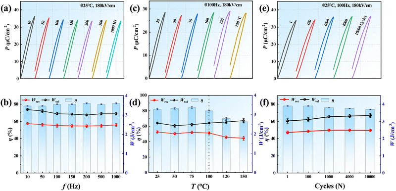
In practical applications of dielectric energy storage capacitors, good frequency and temperature stabilities, and fatigue resistance are critical. Thus, it is necessary to further explore these characteristics. Fig. 11(a) displays the unipolar P–E loops of BNBT–0.14CHZ ceramics from 10 Hz to 1000 Hz at RT and 180 kV cm−1. The curves clearly maintain a slim shape. The corresponding Wrec and η shown in Fig. 11(b), exhibit only slight fluctuation (<4%), indicating good frequency stability. Fig. 11(c) displays the unipolar P–E loops of BNBT–0.14CHZ ceramics from 25 °C to 150 °C at 180 kV cm−1 and 100 Hz. Fig. 11(d) shows good temperature stability with a variation of Wrec < 2.3% at T ≤ 100 °C, while they are degraded at T > 100 °C, which might be attributed to the enhanced domain switching polarization as well as increased the conduction loss at high temperature.52Fig. 11(e) displays the unipolar P–E loops of BNBT–0.14CHZ ceramics from 1 to 104 cycles at 180 kV cm−1 and 100 Hz. With the rise of cycle numbers, Pm increases slightly, while the fluctuations of Wrec and η are less than ∼5.1% and ∼2.3%, respectively, as shown in Fig. 11(f), suggesting a good fatigue resistance.
The underdamped pulsed discharge electric current–time curves as a function of electric field were investigated to reveal the actual energy discharge behavior of BNBT–0.14CHZ, as depicted in Fig. 12(a). The corresponding current density (CD = Imax/S, where S is the effective electrode area) and power density (PD = EImax/2S) under various E are illustrated in Fig. 12(b). CD and PD are ∼499.6 A cm−2 and ∼25.0 MW cm−3 at 100 kV cm−1, respectively. The overdamped discharge curves under various E are shown in Fig. 12(c), and the corresponding discharge energy density can be calculated by the equation:  where I, t, R (100 Ω in this paper), and V are the current value, time, load resistance, and volume, respectively, as plotted in Fig. 12(d). Note that under the same E, Wdis is smaller than Wrec, which is attributed to domain clamping caused by the more energy loss during charge and discharge testing. Moreover, the discharge time t0.9 (corresponding to the time of 90% energy releasing) is ∼72 ns. The fast discharge rate should be mainly ascribed to the existence of highly dynamic nanodomains featuring a fast polarization response to the applied electric field. The high PD, Wdis values and a short t0.9 indicate that the BNBT–0.14CHZ ceramics are promising candidates for pulsed power system applications.
4. Conclusion
In summary, BNBT–xCHZ ceramics were successfully designed by a synergistic optimization strategy. The incorporation of BT into NBT to construct MPB was helpful to sustain a high Pm, while the addition of CHZ optimized the microstructure, refined the grain size, reduced Pr, narrowed the hysteresis loops, and formed PNRs. Consequently, a giant Wrec of ∼5.09 J cm−3 and a large ΔP of ∼42.5 μC cm−2 were obtained simultaneously in BNBT–0.14CHZ ceramics at 283 kV cm−1. In addition, good frequency stability from 10 Hz to 1000 Hz, good temperature stability from 25 °C to 150 °C, excellent fatigue resistance among 1–104 cycles and a fast discharge time of ∼72 ns were achieved. These results suggested that the BNBT–0.14CHZ ceramics could be a promising material to use in high-energy storage dielectric capacitors applications.Data availability
All data is presented in the form of charts in the paper.Conflicts of interest
There are no conflicts to declare.Acknowledgements
This work was supported by the Funding by Science and Technology Projects in Guangzhou (202201000008), the Natural Science Foundation of Guangdong Province of China (2024A1515012484), the Guangdong Provincial Key Laboratory (2020B1212060066), the Young Innovative Talent Project in Higher Education of Guangdong Province (2023KQNCX162), Guangdong Basic and Applied Basic Research Foundation (2022A1515110515), the Applied Basic Research Foundation of Guangdong Province (Grant No. 2022A1515011530), and the Shenzhen Natural Science Fund (Stable Support Plan Program, Grant No. GXWD20220818165637002).References
- H. B. Zhang, T. Wei, Q. Zhang, W. G. Ma, P. Y. Fan, D. Salamon, S. T. Zhang, B. Nan, H. Tan and Z. G. Ye, A review on the development of lead-free ferroelectric energy-storage ceramics and multilayer capacitors, J. Mater. Chem. C, 2020, 8, 16648–16667 RSC
.
- G. Wang, Z. L. Lu, Y. Li, L. H. Li, H. F. Ji, A. Feteira, D. Zhou, D. W. Wang, S. J. Zhang and L. M. Reaney, Electroceramics for High-Energy Density Capacitors: Current Status and Future Perspectives, Chem. Rev., 2021, 121, 6124–6172 CrossRef CAS PubMed
.
- Y. Lin, D. Li, M. Zhang and H. B. Yang, (Na0.5Bi0.5)0.7Sr0.3TiO3 modified by Bi(Mg2/3Nb1/3)O3 ceramics with high energy-storage properties and an ultrafast discharge rate, J. Mater. Chem. C, 2020, 8, 2258–2264 RSC
.
- L. M. Chen, J. Zhou, L. Z. Xu, J. X. Ding, Z. M. Sun, Q. H. Bao and X. H. Hao, Achieving ultra-short discharge time and high energy density in lead-based antiferroelectric ceramics by A-site substitution, Chem. Eng. J., 2022, 447, 137367 CrossRef CAS
.
- S. Y. Zhou, Y. P. Pu, X. Q. Zhang, Y. Shi, Z. Y. Gao, Y. Feng, G. D. Shen, X. Y. Wang and D. W. Wang, High energy density, temperature stable lead-free ceramics by introducing high entropy perovskite oxide, Chem. Eng. J., 2022, 427, 131684 CAS
.
- W. Huang, Y. Chen, X. Li, G. S. Wang, J. K. Xia and X. L. Dong, Superior energy storage performances achieved in (Ba,Sr)TiO3-based bulk ceramics through composition design and Core-shell structure engineering, Chem. Eng. J., 2022, 444, 135523 CAS
.
- Z. Y. Ma, Y. Li, Y. Zhao, N. N. Sun, C. X. Lu, P. Han, D. W. Wang, Y. H. Hu, X. J. Lou and X. H. Hao, High-performance energy-storage ferroelectric multilayer ceramic capacitors via nano-micro engineering, J. Mater. Chem. A, 2023, 11, 7184–7192 CAS
.
- Z. H. Dai, J. L. Xie, Z. B. Chen, S. Zhou, J. J. Liu, W. G. Liu, Z. Z. Xi and X. B. Ren, Improved energy storage density and efficiency of (1 − x)Ba0.85Ca0.15Zr0.1Ti0.9O3−xBiMg2/3Nb1/3O3 lead-free ceramics, Chem. Eng. J., 2021, 410, 128341 CrossRef CAS
.
- C. Y. Luo, Y. Z. Wei, Q. Feng, M. Wang, N. N. Luo, C. L. Yuan, C. R. Zhou, T. Fujita and J. W. Xu, Significantly enhanced energy-storage properties of Bi0.47Na0.47Ba0.06TiO3–CaHfO3 ceramics by introducing Sr0.7Bi0.2TiO3 for pulse capacitor application, Chem. Eng. J., 2022, 429, 132165 CrossRef CAS
.
- J. H. Zhao, Z. B. Pan, L. M. Tang, Y. H. Shen, X. Q. Chen, H. H. Li, P. Li, Y. Zhang, J. J. Liu and J. W. Zhai, Greatly enhanced discharged energy density and efficiency of BiFeO3-based ceramics by regulating insulation performance, Mater. Today Phys., 2022, 27, 100821 CrossRef CAS
.
- X. B. Zhang, G. S. Chen, Z. X. Liu, X. L. Miao, Z. H. Zhang, D. Y. Chen, K. H. Lam, M. Zeng, X. S. Gao and J. M. Liu, Achieving ultrahigh energy storage density under low electric field in (Na0.5Bi0.5)TiO3-based relaxor ferroelectric ceramics via a synergistic optimization strategy, Chem. Eng. J., 2024, 480, 147973 CrossRef CAS
.
- X. S. Qiao, D. Wu, F. D. Zhang, B. Chen, X. D. Ren, P. F. Liang, H. L. Du, X. L. Chao and Z. P. Yang, Bi0.5Na0.5TiO3-based relaxor ferroelectric ceramic with large energy density and high efficiency under a moderate electric field, J. Mater. Chem. C, 2019, 7, 10514–10520 RSC
.
- C. Y. Luo, Q. Feng, N. N. Luo, C. L. Yuan, C. R. Zhou, Y. Z. Wei, T. Fujita, J. W. Xu and G. H. Chen, Effect of Ca2+/Hf4+ modification at A/B sites on energy-storage density of Bi0.47Na0.47Ba0.06TiO3 ceramics, Chem. Eng. J., 2021, 420, 129861 CrossRef CAS
.
- W. J. Cao, L. Li, H. Y. Zhao, C. Y. Wang, C. Liang, F. Li, X. C. Huang and C. C. Wang, Outstanding energy storage performance of NBT-based ceramics under moderate electric field achieved via antiferroelectric engineering, ACS Appl. Mater. Interfaces, 2023, 15, 38633–38643 CrossRef CAS
.
- H. H. Nie, L. M. Ruan, L. Hu, X. R. Wang, F. K. Chen, S. Zhou, Y. Y. Wang, T. T. Ai, Y. Yan and G. Liu, Enhanced dielectric energy storage performance of A-site Ca2+-doped Na0.5Bi0.5TiO3–BaTiO3–BiFeO3 Pb-free ceramics, Ceram. Int., 2022, 48, 21061–21070 CrossRef CAS
.
- M. Acosta, J. D. Zang, W. Jo and J. Roedel, High-temperature dielectrics in CaZrO3-modified Bi1/2Na1/2TiO3-based lead-free ceramics, J. Eur. Ceram. Soc., 2012, 32, 4327–4334 CrossRef CAS
.
- L. Zhang, Y. P. Pu, M. Chen, F. P. Zhuo, C. Dietz and T. Froemling, Decreasing polar-structure size: achieving superior energy storage properties and temperature stability in Na0.5Bi0.5TiO3-based ceramics for low electric field and high-temperature applications, J. Eur. Ceram. Soc., 2021, 41, 5890–5899 CrossRef CAS
.
- Z. X. Liu, C. A. Wang, X. B. Zhang, G. S. Chen, A. H. Zhang, M. Zeng, D. Y. Chen, Z. P. Hou, Z. Fan, M. H. Qin, X. B. Lu, X. S. Gao and J. M. Liu, Ultrahigh polarization response along large energy storage properties in BiFeO3–BaTiO3-based relaxor ferroelectric ceramics under low electric field, ACS Appl. Mater. Interfaces, 2022, 14, 53690–53701 CrossRef CAS
.
- X. S. Qiao, D. Wu, F. D. Zhang, M. S. Niu, B. Chen, X. M. Zhao, P. F. Liang, L. L. Wei, X. L. Chao and Z. P. Yang, Enhanced energy density and thermal stability in relaxor ferroelectric Bi0.5Na0.5TiO3–Sr0.7Bi0.2TiO3 ceramics, J. Eur. Ceram. Soc., 2019, 39, 4778–4784 CAS
.
- D. Hu, Z. B. Pan, X. Zhang, H. R. Ye, Z. Y. He, M. K. Wang, S. Xing, J. W. Zhai, Q. Fu and J. J. Liu, Greatly enhanced discharge energy density and efficiency of novel relaxation ferroelectric BNT-BKT-based ceramics, J. Mater. Chem. C, 2020, 8, 591–601 CAS
.
- L. Zheng, P. C. Sun, P. Zheng, W. F. Bai, L. L. Li, F. Wen, J. J. Zhang, N. N. Wang and Y. Zhang, Significantly tailored energy-storage performances in Bi0.5Na0.5TiO3–SrTiO3-based relaxor ferroelectric ceramics by introducing bismuth layer-structured relaxor BaBi2Nb2O9 for capacitor application, J. Mater. Chem. C, 2021, 9, 5234–5243 CAS
.
- Y. C. Wu, Y. Z. Fan, N. T. Liu, P. Peng, M. X. Zhou, S. G. Yan, F. Cao, X. L. Dong and G. S. Wang, Enhanced energy storage properties in sodium bismuth titanate-based ceramics for dielectric capacitor applications, J. Mater. Chem. C, 2019, 7, 6222–6230 RSC
.
- J. H. Wang, Y. Li, N. N. Sun, J. H. Du, Q. W. Zhang and X. H. Hao, Bi(Mg0.5Ti0.5)O3 addition induced high recoverable energy-storage density and excellent electrical
properties in lead-free Na0.5Bi0.5TiO3-based thick films, J. Eur. Ceram. Soc., 2019, 39, 255–263 CrossRef CAS
.
- D. D. Wang, J. Y. Zhu, Z. X. Liu, A. H. Zhang, C. A. Wang, C. M. Leung, X. S. Gao, X. B. Lu and M. Zeng, Enhanced energy storage performance in (1 − x)Bi0.85Sm0.15FeO3−xCa0.5Sr0.5Ti0.9Zr0.1O3 relaxor ceramics, J. Alloys Compd., 2022, 903, 163888 CrossRef CAS
.
- Y. Li, G. C. Wang, A. Gong, S. Zhang, J. Liu, N. N. Sun and X. H. Hao, High-Performance Ferroelectric Electromagnetic Attenuation Materials with Multiple Polar Units Based on Nanodomain Engineering, Small, 2022, 18, 2106302 CrossRef CAS PubMed
.
- B. K. Chu, J. G. Hao, P. Li, Y. C. Li, W. Li, L. M. Zheng and H. R. Zeng, High-energy storage properties over a broad temperature range in La-modified BNT-based lead-free ceramics, ACS Appl. Mater. Interfaces, 2022, 14, 19683–19696 CrossRef CAS
.
- B. Yan, K. P. Chen and L. A. An, Design and preparation of lead-free (Bi0.4Na0.2K0.2Ba0.2)TiO3–Sr(Mg1/3Nb2/3)O3 high-entropy relaxor ceramics for dielectric energy storage, Chem. Eng. J., 2023, 453, 139921 CrossRef CAS
.
- L. N. Shi, Y. G. Wang, Z. H. Ren, A. Jain, S. S. Jiang and F. G. Chen, Significant improvement in electrical characteristics and energy storage performance of NBT-based ceramics, Ceram. Int., 2022, 48, 37494 CrossRef CAS
.
- L. N. Shi, Z. H. Ren, A. Jain, R. H. Jin, S. S. Jiang, H. Z. Zhou, F. G. Chen and Y. G. Wang, Enhanced energy storage performance achieved in Na0.5Bi0.5TiO3–Sr0.7Bi0.2TiO3 ceramics via domain structure and bandgap width tuning, Ceram. Int., 2023, 49, 12822–12831 CrossRef CAS
.
- W. J. Shi, Y. L. Yang, L. Y. Zhang, R. Y. Jing, Q. Y. Hu, D. O. Alikin, V. Y. Shur, J. H. Gao, X. Y. Wei and L. Jin, Enhanced energy storage performance of eco-friendly BNT-based relaxor ferroelectric ceramics via polarization mismatch-reestablishment and viscous polymer process, Ceram. Int., 2022, 48, 6512–6519 CrossRef CAS
.
- X. Li, X. Y. Dong, F. Wang, Z. Tan, Q. M. Zhang, H. Chen, J. W. Xi, J. Xing, H. F. Zhou and J. G. Zhu, Realizing excellent energy storage properties in Na0.5Bi0.5TiO3-based lead-free relaxor ferroelectrics, J. Eur. Ceram. Soc., 2022, 42, 2221–2229 CrossRef CAS
.
- B. Yang, J. Y. Zhang, X. J. Lou, Y. F. Gao, P. Shi, Y. D. Yang, M. Yang, J. Cui, L. L. Wei and S. D. Sun, Enhancing comprehensive energy storage properties in tungsten bronze Sr0.53Ba0.47Nb2O6-based lead-free ceramics by B-site doping and relaxor tuning, ACS Appl. Mater. Interfaces, 2022, 30, 34855–34866 CrossRef
.
- B. Yang, Y. F. Gao, X. J. Lou, Y. D. Yang, Y. H. Hu, G. J. Zhang and S. D. Sun, Remarkable energy storage performances of tungsten bronze Sr0.53Ba0.47Nb2O6-based lead-free relaxor ferroelectric for high-temperature capacitors application, Energy Storage Mater., 2023, 55, 763–772 CrossRef
.
- D. Li, Y. Lin, M. Zhang and H. B. Yang, Achieved ultrahigh energy storage properties and outstanding charge–discharge performances in (Na0.5Bi0.5)0.7Sr0.3TiO3-based ceramics by introducing a linear additive, Chem. Eng. J., 2020, 392, 123729 CrossRef CAS
.
- F. Yan, Y. J. Shi, X. F. Zhou, K. Zhu, B. Shen and J. W. Zhai, Optimization of polarization and electric field of bismuth ferrite-based ceramics for capacitor applications, Chem. Eng. J., 2021, 417, 127945 CrossRef CAS
.
- G. Liu, Y. Li, B. Guo, M. Y. Tang, Q. Li, J. Dong, L. J. Yu, K. Yu, Y. Yan and D. W. Wang, Ultrahigh dielectric breakdown strength and excellent energy storage performance in lead-free barium titanate-based relaxor ferroelectric ceramics via a combined strategy of composition modification, viscous polymer processing, and liquid-phase sintering, Chem. Eng. J., 2020, 398, 125625 CrossRef CAS
.
- G. F. Liu, L. Chen, H. F. Yu, Z. F. Zhang, J. Wu, C. Zhou, H. Qi and J. Chen, High energy-storage performance in multiple roles modified NaNbO3–Ba(Fe0.5Nb0.5)O3 lead-free relaxors, Chem. Eng. J., 2023, 474, 145705 CrossRef CAS
.
- H. B. Yang, J. H. Tian, Y. Lin and J. Q. Ma, Realizing ultra-high energy storage density of lead-free 0.76Bi0.5Na0.5TiO3–0.24SrTiO3–Bi(Ni2/3Nb1/3)O3 ceramics under low electric fields, Chem. Eng. J., 2021, 418, 129337 CrossRef CAS
.
- J. F. Lin, G. L. Ge, K. Zhu, H. R. Bai, B. S. Sa, F. Yan, G. H. Li, C. Shi, J. W. Zhai, X. Wu and Q. W. Zhang, Simultaneously achieving high performance of energy storage and transparency via A-site non-stoichiometric defect engineering in KNN-based ceramics, Chem. Eng. J., 2022, 444, 136538 CrossRef CAS
.
- K. Wei, J. H. Duan, X. F. Zhou, G. S. Li, D. Zhang and H. Li, Achieving ultrahigh energy storage performance for NaNbO3-based lead-free antiferroelectric ceramics via the coupling of the stable antiferroelectric R phase and nanodomain engineering, ACS Appl. Mater. Interfaces, 2023, 15, 48354–48364 CrossRef CAS
.
- M. S. Wang, A. W. Xie, J. Fu and R. Z. Zuo, Energy storage properties under moderate electric fields in BiFeO3-based lead-free relaxor ferroelectric ceramics, Chem. Eng. J., 2022, 440, 135789 CrossRef CAS
.
- P. Shi, X. P. Zhu, X. J. Lou, B. Yang, Q. D. Liu, C. C. Kong, S. Yang, L. Q. He, R. R. Kang and J. T. Zhao, Tailoring ferroelectric polarization and relaxation of BNT-based lead-free relaxors for superior energy storage properties, Chem. Eng. J., 2022, 428, 132612 CrossRef CAS
.
- Q. F. Chen, T. T. Gao, R. Lang, Z. Tan, J. Xing and J. G. Zhu, Achieving outstanding temperature stability in KNN-based lead-free ceramics for energy storage behavior, J. Eur. Ceram. Soc., 2023, 43, 2442–2451 CrossRef CAS
.
- Q. J. Li, S. S. Ji, D. D. Wang, J. Y. Zhu, L. Y. Li, W. Wang, M. Zeng, Z. P. Hou, X. S. Gao, X. B. Lu, Q. L. Li and J. M. Liu, Simultaneously enhanced energy storage density and efficiency in novel BiFeO3-based lead-free ceramic capacitors, J. Eur. Ceram. Soc., 2021, 41, 387–393 CrossRef CAS
.
- S. Li, T. F. Hu, H. C. Nie, Z. Q. Fu, C. H. Xu, F. F. Xu, G. S. Wang and X. L. Dong, Giant energy density and high efficiency achieved in silver niobate-based lead-free antiferroelectric ceramic capacitors via domain engineering, Energy Storage Mater., 2021, 34, 417–426 CrossRef
.
- S. Liu, W. W. Feng, J. H. Li, B. He, M. T. Liu, Z. D. Bao, D. J. Luo and C. C. Zhao, Realizing excellent energy storage performance and fatigue endurance in Sr0.7Sm0.2TiO3 modified 0.67BiFeO3–0.33BaTiO3 lead-free relaxor ceramics, J. Eur. Ceram. Soc., 2022, 42, 7430–7440 CrossRef CAS
.
- S. Liu, W. W. Feng, J. H. Li, C. C. Zhao, C. Hu, B. He, Z. D. Bao and X. Z. Luan, Achieving high energy storage density and efficiency simultaneously in Sr(Nb0.5Al0.5)O3 modified BiFeO3 based lead-free ceramics, Chem. Eng. J., 2023, 451, 138916 CrossRef CAS
.
- T. Y. Li, P. F. Chen, F. Li and C. C. Wang, Energy storage performance of Na0.5Bi0.5TiO3–SrTiO3 lead-free relaxors modified by AgNb0.85Ta0.15O3, Chem. Eng. J., 2021, 406, 127151 CrossRef CAS
.
- Y. Pan, X. Wang, Q. P. Dong, J. M. Wang, H. Y. Chen, X. Y. Dong, L. Deng, H. L. Zhang, X. L. Chen and H. F. Zhou, Enhanced energy storage properties of Bi(Ni2/3Nb1/6Ta1/6)O3–NaNbO3 solid solution lead-free ceramics, Ceram. Int., 2022, 48, 26466–26475 CrossRef CAS
.
- Z. P. Wang, R. R. Kang, W. Y. Liu, L. X. Zhang, L. Q. He, S. Y. Zhao, H. X. Duan, Z. H. Yu, F. Kang, Q. Z. Sun, T. R. Zhang, P. Mao, J. P. Wang and L. Zhang, (Bi0.5Na0.5)TiO3-based relaxor ferroelectrics with medium permittivity featuring enhanced energy-storage density and excellent thermal stability, Chem. Eng. J., 2022, 427, 131989 CrossRef CAS
.
- L. Chen, F. X. Long, H. Qi, H. Liu, S. Q. Deng and J. Chen, Outstanding energy storage performance in high-hardness (Bi0.5K0.5)TiO3-based lead-free relaxors via multi-scale synergistic design, Adv. Funct. Mater., 2022, 32, 2110478 CrossRef CAS
.
- N. N. Sun, J. H. Du, Y. Zhao, C. X. Lu, P. Han, Y. Li, Q. W. Zhang and X. H. Hao, Flexible multilayer lead-free film capacitor with high energy storage performances via heterostructure engineering, J. Materiomics, 2022, 8, 772–780 CrossRef
.
Footnote |
| † Electronic supplementary information (ESI) available. See DOI: https://doi.org/10.1039/d4tc03558e |
| This journal is © The Royal Society of Chemistry 2025 |

