
Weak Fermi level pinning and low barrier interfacial contact: 2D lead-free perovskites on multilayer GaN†
Pengjie
Fu
a,
Baolin
Wang
 b,
Mengni
Liu
a,
Guixian
Ge
a,
Juan
Hou
*a and
Xiaodong
Yang
*a
b,
Mengni
Liu
a,
Guixian
Ge
a,
Juan
Hou
*a and
Xiaodong
Yang
*a
aCollege of Sciences, Shihezi University, Shihezi 832003, China. E-mail: hjuan05@sina.com; yangxiaodong1209@hotmail.com
bCollege of Physical Science and Technology, Nanjing Normal University, Nanjing 210093, China
First published on 21st October 2024
Abstract
Metal halide perovskites (MHPs) have shown great potential in photovoltaic and electronic fields due to their high charge carrier mobility, adjustable band gap and extremely high absorption coefficient. The formation of a type-II band alignment heterojunction between a perovskite and an electron transport layer is a commonly used method to enhance electron transport. However, traditional heterojunctions have strong Fermi level pinning (FLP) and high contact potential barriers that limit electron transfer efficiency. In this work, we report a novel semiconductor–semiconductor junction (SSJ) based on MHPs to simultaneously address the limitations of potential barriers and FLP on electron transport. By integrating Ba2+ passivated 2D lead-free perovskites with GaN nanosheets to construct the Ba–CsSrI3/GaN SSJ, we eliminate high potential barriers and overcome interfacial gap states to achieve effective carrier migration. It is found that the negative electron affinity (NEA) formed at the Ba/GaN (0001) interface eliminates the adverse effects of interface dipole moments, allowing electrons to spontaneously cross the interface through GaN layers. The Schottky–Mott rule proves that the FLP is controlled within a very small range. In addition, as the number of GaN layers increases, the NEA at the interface remains unchanged and the type-II band alignment changes to a zero band gap while still maintaining the ability to extract electrons, forming a low barrier contact with a high conductivity of 7.79 × 10³ S cm−1. These findings demonstrate the significant potential of GaN as the electron transport layer of the Ba–CsSrI3 perovskite in applications such as photovoltaic devices, photodetectors, and integrated circuits.
1. Introduction
Two-dimensional (2D) metal halide perovskites (MHPs) have attracted much attention in recent years due to their wide substrate compatibility, tunable band gaps and anisotropic charge transport.1–5 The practical application of 2D Cs-based MHPs (e.g., CsPbX3, CsCaX3 and CsSrX3 X = Cl, Br, I)6–8 in devices requires direct contact with the electron transport layer to form type-II band alignment to enhance electron uptake.9 Although n-type perovskites enhance electron extraction in regular solar cells,10 they can cause instability and charge accumulation in perovskite solar cells,11,12 and the reverse electric field generated by the depletion region may form high potential barriers. Generally speaking, the formation of a semiconductor–semiconductor junction (SSJ) between traditional metal oxides and 2D MHPs typically results in the interface barrier and Fermi level pinning (FLP), which reduce carrier migration efficiency, increase contact resistance, and lower device conductivity.13,14 It should be noted that, regardless of the type of contact, 2D MHPs cannot avoid the formation of FLP,15 and their excellent optoelectronic properties are masked by high interface barriers and strong FLP. Therefore, designing interfaces that simultaneously address two major contact issues is crucial for photovoltaic devices,16–18 photodetectors,19 and integrated circuit applications.20Due to the lack of effective methods to address the interface barrier, the efficiency of electron transport at the interface based on 2D materials is generally considered to be dominated by the contact resistance, which is mainly produced by the van der Waals (vdW) gap at the contact interface.21 In addition, the potential barrier may be generated by the depletion region22 at the interface of semiconductor heterojunctions, which charge carriers must overcome to cross the interface. As reported by Wang et al., energy barriers can be created between perovskite grains and other wide bandgap materials (e.g., PbI2 and the 2D perovskite phase) at grain boundaries.23 PbI2 and 2D perovskite phases at grain boundaries can significantly influence charge recombination and obstruct charge transport in 2D perovskite films,24 and charges are usually confined within inorganic frameworks due to strong quantum and dielectric confinement effects.25 When charges reach the heterointerfaces, they will be reflected back to the perovskite grains due to the presence of energy barriers, which decrease carrier transport at the grain boundaries. A deployed solution is to increase the number of semiconductor layers perpendicular to the semiconductor heterojunction to adjust the barrier height and form a zero bandgap contact surface.26 However, this transformation only eliminates the energy barrier and does not reduce the impact of Fermi level pinning (FLP) on charge transfer efficiency, thereby limiting the application of optoelectronic devices.
The FLP effect means that the Fermi energy level no longer varies with external injection of electrons (for example, the carriers provided by dopants cannot be activated). An interface gap state (IGS) is one of the main contributors to FLP.15 Although the type-II band alignment formed by semiconductor heterojunctions enhances the separation of electron–hole pairs, the IGS generated at the contact interface limits the charge transfer efficiency.27 The IGS will lead to the recombination of electrons and holes during the separation process, which is specifically reflected in the deep levels of a band structure.28 Xiang et al. have demonstrated that the selective passivation of the SnO2/CsPbI3 heterojunction interface through Mg and Cl doping effectively eliminates the IGS.29 However, although the dipole interaction at the interface avoids electron–hole recombination,30 the depletion layers are formed due to the charge accumulation effect.31 Therefore, there is an urgent need to find a method to simultaneously improve the adverse effects of the IGS and interface dipole moment.
The negative electron affinity (NEA), which is an effective method to enhance electron emitting and carrier extraction efficiency,32 has been widely used in wide bandgap semiconductors, such as GaN and ZnO.33 Among them, experiments have revealed that PSCs with GaN substrates as electron transport layers can further improve the energy conversion efficiency.34–36 This makes NEA possible as an effective solution for enhancing electron transport at the interface. Typically, NEA can be achieved by forming a strong dipole moment on the surface of semiconductors.37 This requires us to find an interface with a strong polarity to induce NEA through interface coupling between 2D MHPs and electron transport layers. The formation of NEA will generate electron tunneling, allowing electrons to migrate spontaneously. Compared with traditional semiconductor heterojunctions, it may lead to significant changes in electronic and optical properties. The NEA is expected to become the key to simultaneously solving the pinning effect and improving the charge transfer efficiency of perovskite heterojunctions.
In this work, we report for the first time a new structure of a SSJ that reduces the high potential barrier and FLP by integrating the Ba2+ passivated lead-free perovskite (Ba–CsSrI3) on GaN nanosheets based on density functional theory (DFT) calculations. The NEA effect is due to the large dipole moment at the Ba/GaN (0001) interface, which allows electrons to cross the interface spontaneously, which successfully mitigates the adverse impact of the reversed electric field on the semiconductor interface. As the number of GaN layers increases, the NEA effect has remained consistent, while the band gap gradually vanishes and the calculated pinning factor slope increases to 0.97, approaching the Schottky–Mott limit, thereby achieving strong electron transfer. The synergistic effect of NEA and Fermi level shifting formed in the Ba–CsSrI3/GaN heterostructure simultaneously addresses the drawbacks of the high potential barrier and FLP, leading to enhanced electron transport efficiency with a maximum conductivity of up to 7.79 × 10³ S cm−1.
2. Computational details
All DFT calculations were performed by using the Vienna ab initio simulation package (VASP).38 The interaction between the valence electrons and the core electrons was treated by the projector augmented wave (PAW)39 method. A kinetic energy cutoff of 500 eV was used for plane-wave propagation, and it ensured sufficient computational accuracy. The electron exchange–correlation energy was treated by using the meta-generalized-gradient approximation (meta-GGA)40 of the strongly constrained and appropriately normed (SCAN) functional. The interface interactions of vdW heterostructures were described by using the SCAN functional with vdW correction (DFT-D3).41 For the plate with a net dipole moment, dipole correction was considered in all calculations. K-point sampling in the first Brillouin zone was achieved using the Gamma-centric Monkhorst–Pack scheme, with a grid of 8 × 8 × 1 for 2D MHPs and vdW heterostructures. A vacuum layer of about 20 Å was introduced along the Z direction to avoid the false interaction between adjacent plates. For geometric optimization, the convergence criteria of energy and force acting on each atom were set to be 10−7 eV and 10−5 eV Å−1, respectively.In order to find an accurate calculation method suitable for heterojunction systems, we compared the bandgaps of CsPbI3 and GaN calculated using PBE, SOC, HSE + SOC,42 and meta-GGA (Fig. S1 and Table S1, ESI†). It can be seen that the band gaps of CsPbI3 and GaN calculated by the SCAN meta-GGA method are consistent with the experimental and theoretical reports. In contrast, PBE and SOC led to significant underestimation of the bandgaps of CsPbI3 and GaN, while HSE + SOC overestimates the bandgap. Therefore, the meta-GGA method was used to predict the electronic properties of 2D MPHs and GaN nanosheets and their heterostructures.
3. Results and discussion
3.1 Structural stability of the 2D Ba–CsSrI3/GaN heterojunction
We first address the structural stabilities and electronic properties of the 2D perovskite and GaN, which are crucial for understanding the construction of MHP/GaN heterostructures. Fig. 1(a) shows the atomic structure of the 2D perovskite, which is obtained from a cubic CsSrI3 along the (111) direction. However, the band structure and projected density of states (PDOS) of 2D CsSrI3(111) (i.e. Cs4Sr3I12) have impurity energy levels (Fig. 1(b)), which is due to the instability of the structure caused by the high surface energy resulting from the surface dangling bond. By comparing different doping methods (Fig. S2 and Table S2, ESI†), the replacement of the outermost Cs+ cations by divalent cations (such as Ba2+, Sn2+, and Sr2+) was regarded as the most efficient method to improve the stability of 2D CsSrI3, resulting in a significant decrease in surface energy indicating that the stability of the 2D perovskite is improved. The surface energy of the divalent Ba2+ doped structure was −32.44 meV Å−2, lower than that of the trivalent doped structure (−19.55 meV Å−2) (Tables S2 and S3, ESI†). The formula for calculating the surface energy is as follows: | (1) |
 | ||
| Fig. 1 (a) The side view of the atomic structure of the 2D CsSrI3(111) perovskite. The band structure and PDOS of (b) non-passivated and (c) passivated perovskites with Ba. (d) The optimized geometric structure of the Ba–CsSrI3/GaN heterostructure. The band structure and PDOS of (e) 2D Ba–CsPbI3/GaN and (f) 2D Ba–CsSrI3/GaN. Cs, I, Ga, N, H, Ba, and Sr atoms are displayed in cyan, purple, green, blue and white, light blue and yellow, respectively. The orange lines represent impurity energy levels. | ||
The stabilities of 2D perovskites can be further verified by the result of band structures. We found that the band structures of pristine perovskite nanosheets and those surface-passivated with Sn, Mg, Ca, and Zn all contain deep defect levels (Fig. S3, ESI†), which originate from unpaired electrons of surfaces. The substitution of Cs+ cations with Ba2+ at the surface layer eliminates surface states, leading to a recovery of the intrinsic semiconductor band structure and PDOS (Fig. 1(c)), and Ba atom doping has been widely used to improve the stability of perovskite materials.43–45 Moreover, the Ba atom has a similar radius to the Cs atom, making it an ideal choice for forming a stable 2D perovskite. For 2D GaN nanosheets, due to the existence of dangling bonds (Fig. S4(a), ESI†), their surfaces were passivated by hydrogen to eliminate the suspended bonds (Fig. S4(b), ESI†). In order to enhance the efficiency of electron transport, we also compared the stability of other common perovskites (e.g., CsPbI3) and GaN composites. By observing their band structures and PDOS (Fig. 1(e), (f) and Fig. S5, ESI†), it is found that impurity energy levels exist in substitutions other than Sr2+, which formed a lead-free perovskite with impurity-free energy levels. And, the replacement of Pb2+ with Sr2+ in perovskites has been widely used in light-emitting devices.46
Based on the above choices and comparisons, the 2D Ba–CsSrI3/GaN heterostructure was constructed with a small lattice mismatch (∼0.84%) between the (1 × 1) Ba–CsSrI3 and  GaN nanosheets. In addition, according to the arrangement direction of GaN, the Ba–CsSrI3/GaN heterojunction can be constructed in two different ways, including Ga-top and N-top configurations based on the relative position between GaN and Ba–I termination at the interface (Fig. S6, ESI†). To further determine the stability of the heterojunction, the most stable interfacial configurations were evaluated by elastic stiffness constants Cij (Table S4, ESI†). The Ba–CsSrI3/GaN heterostructure exhibits triclinic symmetry, resulting in thirty-six independent elastic constants as follows:
 | (2) |
Based on the criteria of mechanical stability, we found that the Ga-top configuration of the Ba–CsSrI3/GaN heterostructure is mechanically stable, while the N-top configuration is unstable (Table S4, ESI†). In addition, we also compared the surface energies of different GaN layers and heterojunction formation energies (Tables S5 and S6, ESI†). Our findings indicate that the Ba–CsSrI3/GaN heterostructure remains stable and reasonable when the number of GaN layers (n) is three or greater. Consequently, we will utilize the Ga-terminated Ba–CsSrI3/GaN structure with trilayer GaN (n = 3) as a critical structure for studying and analyzing electron transport properties, as shown in Fig. 1(d).
3.2 Interface dipole and the NEA effect of the 2D Ba–CsSrI3/GaN heterojunction
The interface of the perovskite heterojunction is usually accompanied by the aggregation of electrons and holes to form the interface dipole moment (i.e. depletion/barrier region), which affects the electron transfer efficiency.21,47 Based on the most stable configuration obtained above, the electron transport of Ba–CsSrI3/GaN is discussed through the electronic structure. Fig. 2(a) shows the projected band structure of the Ba–CsSrI3/GaN heterostructure. The contribution of the projected band indicates that the CBM and VBM states are completely separated in two different layers of the heterostructure, which contributes to the highly efficient separation of electrons and holes, leading to a type-II band alignment. Moreover, this heterostructure exhibits a smaller band gap (1.03 eV) relative to the freestanding Ba–CsSrI3 and GaN nanosheets, which enhances the charge transfer. However, the separation of electrons and holes generates a built-in electric field due to the existence of the dipole moment, which hinders the outward propagation of electrons. To investigate the impact of interface dipole moments on charge transfer in heterojunctions, we calculated the band-edge charges for the heterojunction with the bilayer GaN and dipole moments of heterojunctions with different numbers of GaN layers. Fig. 2(b) shows the charge–density distributions of band-edge states of the Ba–CsSrI3/GaN heterostructure, indicating the regions of electron and hole accumulation. The inset shows the dipole moment principle of the H–GaN substrate formed by Ba activation at the interface. Ba atoms donate part of the electrons to the H–GaN surface to form a [Ban+–GaNn−] dipole moment perpendicular to the surface. Interestingly, direct electron migration is observed at the bottom of the heterojunction by charge–density distributions of band-edge states. Thus, the CBM state of the Ba–CsSrI3/GaN heterostructure includes not only the contribution of GaN nanosheets but also the vacuum layer, implying the possibility of electron excitation directly from the valence band to the vacuum level, resulting in a negative electron affinity effect. Among them, the work function is an important parameter, describing the energy of an electron needed to emit in a vacuum.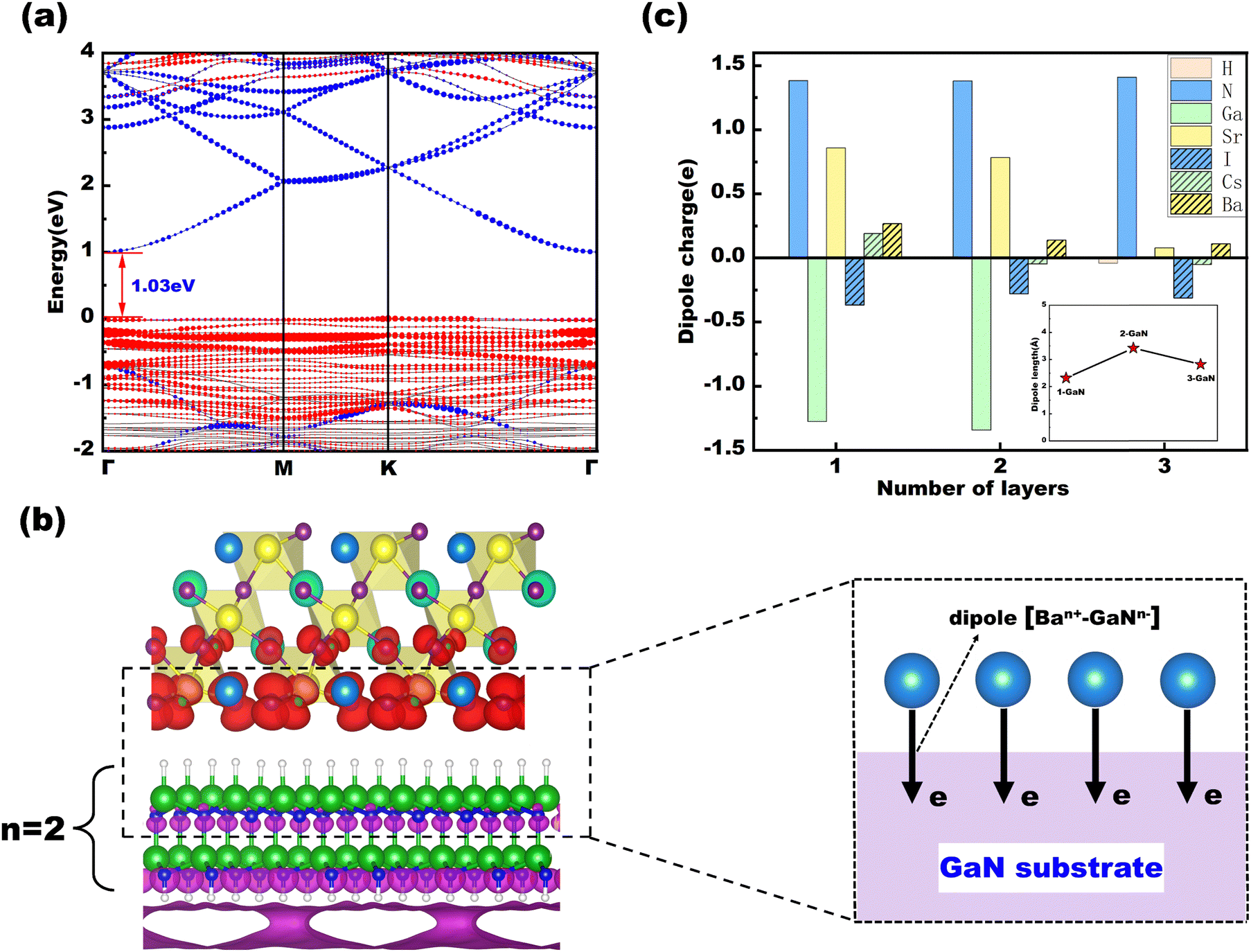 | ||
| Fig. 2 (a) The projected band structure of the Ba–CsSrI3/GaN heterostructure. The blue and red lines in the band structure denote the contribution of GaN and Ba–CsSrI3, respectively. (b) Charge–density distributions of band-edge states of the Ba–CsSrI3/GaN heterojunction. The charge–density distributions contributed by GaN and Ba–CsSrI3 are colored by purple and red, respectively. The inset indicates the schematic diagram of the dipole model during Ba activation on the H–GaN surface. (c) The average dipole charge varying with the layers of GaN from 1 to 3. The inset demonstrates the variation of dipole length with the number of GaN layers. | ||
The work function Φ and electron affinity χ of the heterostructures can be achieved by the following relationships:48
| Φ = Evac − Ef | (3) |
| χ = Evac − Ec | (4) |
It is well-known that the NEA effect originates from a strong dipole moment.49 Therefore, the average positive and negative dipole charge Q± and the average dipole length dz of the interface were analyzed. The formula is as follows:
| Q± = Q+ + Q− | (5) |
 | (6) |
| dz = zBa − zsurface | (7) |
| pz = |Q±| × dz | (8) |
The average dipole charge and average dipole length are plotted in Fig. 2(c). With the increase of GaN layers, the dipole charge of Ga and Sr atoms almost disappeared and changed suddenly, but the total charge difference remains in a certain range with the increase of GaN layers. Meanwhile, the dipole length of the Ba–CsSrI3/GaN heterostructure retains a large value (>2.3 e Å) with the change of layers. Generally, a large dipole moment in the heterojunction tends to restrict charge transfer.50,51 However, at the interface of the Ba–CsSrI3/GaN heterostructure, electron tunneling occurs when the dipole moment is strong enough to eliminate the adverse effect of the reverse electric field on the charge transfer. The formation of the negative electron affinity effect causes electrons to be excited to the vacuum level with only 0.56 eV (Fig. 3(a)). ΔEC represents the conduction band offset between the perovskite and GaN in heterojunctions.
 | ||
| Fig. 3 The (a) schematic band alignment and (b) electrostatic potential distribution of the 2D Ba–CsSrI3/GaN heterostructure (n = 2). (c) Electrostatic potential of the heterostructure (n = 3). The vacuum level, CBM, and Fermi level are indicated by red, green, and blue lines in electrostatic potential distributions, respectively. | ||
Similarly, ΔEV represents the valence band offset. Therefore, the interface interaction of the Ba–CsSrI3/GaN heterostructure plays an important role in charge transfer.
3.3 Low barrier contacts and FLP in the 2D Ba–CsSrI3/GaN heterojunction
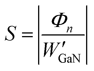
In order to further increase the charge transfer at the contact interface, the barrier should be small enough to increase the carrier transmission probability. The barrier is characterized by two parameters: the height (ΦTB) and width (WTB) of the barrier. The magnitude of the barrier can be inferred from the electrostatic potential at the interface. The low barrier height and narrow width indicate high electron injection efficiency and low contact resistance, where the potential difference between the vdW gap (Φgap) and the potential energy of 2D Ba–CsSrI3/GaN (Φperovskite) is characterized by ΦTB (Fig. 3(b) and (c)). As the number of GaN layers increases, it is found that the ΦTB and WTB values of the heterojunction have significantly decreased (ΦTB from 2.81 eV to 0.44 eV and WTB from 2.42 eV to 0.68 eV) (Fig. S7, ESI†). This indicates that the heterojunction effectively reduces the barrier height and width, forming low barrier contacts and improving electron transfer.As an important factor of FLP, the IGS has been eliminated by doping (Fig. S3 and S4, ESI†). Regardless of the type of heterojunction material, the FLP effect is inevitably encountered.52 Therefore, it is needed to analyze the FLP effect in the Ba–CsSrI3/GaN heterojunction. The existing theoretical basis relies on the magnitude of the pinning factor and the Schottky–Mott limit to predict FLP.53 Encouragingly, recent research has shown that the pinning factor S of Cs0.18FA0.82PbI3/organics interface reaches 1.05, which is close to the Schottky–Mott limit (S = 1).54 However, 2D perovskites and inorganic semiconductor electron transport layers have not yet exhibited such properties. Therefore, it is necessary to study FLP in the Ba–CsSrI3/GaN heterojunction.
To provide a quantitative description of the FLP effect, the FLP strength for a given semiconductor can be calculated using a barrier pinning factor (S):55
 | (9) |
| Φn = WGaN − χ + ΔV | (10) |
 , where WGaN is the work function of 2D GaN, and χ is the electron affinity. The interface dipole ΔV is the result of the charge redistribution at the contact interface. The Schottky–Mott rule can be used to predict the strength of FLP under ideal conditions. The Schottky–Mott rule is obeyed when S = 1. Fig. 4(a) illustrates that the magnitude of the barrier height has linear dependence on the work functions of 2D doped perovskites. In light of eqn 9, S increases from 0.39 to 0.97 with the increase of GaN layers, indicating that FLP is controlled to a very small extent.
 | ||
| Fig. 4 (a) The relative electron barrier height (Φn) of the 2D perovskite/GaN versus work function values of the perovskite surface covered with GaN. S presents the pinning factor. (b) The mechanism and process of low barrier contact transformation. | ||
The above method shows that the increase of GaN layers will weaken the pinning effect of the heterojunction for perovskites. This means that the Ba–CsSrI3/GaN heterojunction not only reduces the interface dipole moment but also eliminates the IGS, greatly limiting the FLP effect, thereby achieving the low potential barrier interface (similar to Ohmic contacts) (Fig. 4(b) and Fig. S8, ESI†). In the meantime, the formation of a zero bandgap does not alter the ability of heterojunctions to extract electrons. Based on the calculated electronic structure, the electrical conductivity, Seebeck coefficients, electrical thermal conductivity and power factor of the Ba–CsSrI3/GaN heterojunction are studied (Fig. S9, ESI†). We found a conductivity of 7.79 × 10³ S cm−1, which is one order of magnitude higher than previous theoretical and experimental studies.56–58 In addition, both CsPbI3 and CsSrI3 can be prepared by the solution method in the experiment,59–61 and the metal surface doping/passivation of perovskites is already very mature.62,63 Therefore, we speculate that Ba doped CsSrI3 perovskites can be prepared using a similar method, which provides theoretical guidance for the preparation of Ba–CsSrI3/GaN perovskite solar cells.
4. Conclusions
In summary, using GaN as an electron transport layer for perovskites simultaneously addresses the limitations of Fermi level pinning and potential barriers to carrier migration. The study results show that the NEA effect can effectively solve the adverse effect of the interface dipole moment on electron transfer. The Ba–CsSrI3/GaN heterojunction eliminates the IGS and weakens the FLP effect through doping, approaching the Schottky–Mott limit. We found that the Ga-top heterojunction performed optimum among all our candidates. The transition to a zero bandgap can be achieved with an increase in the GaN layer, forming a low potential barrier of 0.44 eV. Furthermore, the heterojunction still maintains its ability to extract electrons due to the presence of the NEA effect. The designed heterostructure eliminates the IGS and reduces the interface dipole, overcomes the contact potential bottleneck of the traditional 2D semiconductor heterojunction, and improves the performance of electronic nano-devices, resulting in a high conductivity of 7.79 × 10³ S cm−1. This work provides a novel design approach for electron transport layers in perovskite solar cells.Data availability
The data supporting this article have been included as part of the ESI.†Conflicts of interest
The authors declare that they have no known competing financial interests or personal relationships that could have appeared to influence the work reported in this paper.Acknowledgements
This research is supported by the National Natural Science Foundation of China (Grant No. 12204324).References
- H. Wang, S. Li, X. Liu, Z. Shi, X. Fang and J. He, Low-dimensional metal halide perovskite photodetectors, Adv. Mater., 2021, 33, 2003309 CrossRef CAS
.
- H. Dong, C. Ran, W. Gao, M. Li, Y. Xia and W. Huang, Metal halide perovskite for next-generation optoelectronics: progresses and prospects, eLight, 2023, 3, 3 CrossRef
- J. S. Manser, J. A. Christians and P. V. Kamat, Intriguing optoelectronic properties of metal halide perovskites, Chem. Rev., 2016, 116, 12956–13008 CrossRef CAS PubMed
- G. Kakavelakis, M. Gedda, A. Panagiotopoulos, E. Kymakis, T. D. Anthopoulos and K. Petridis, Metal halide perovskites for high-energy radiation detection, Adv. Sci., 2020, 7, 2002098 CrossRef CAS
- L. Zhang, C. Sun, T. He, Y. Jiang, J. Wei, Y. Huang and M. Yuan, High-performance quasi-2D perovskite light-emitting diodes: from materials to devices, Light: Sci. Appl., 2021, 10, 61 CrossRef CAS PubMed
- M. Suta and C. Wickleder, Spin crossover of Yb2+ in CsCaX3 and CsSrX3 (X = Cl, Br, I)-a guideline to novel halide-based scintillators, Adv. Funct. Mater., 2017, 27, 1602783 CrossRef
- D. Ray, C. Clark, H. Q. Pham, J. Borycz, R. J. Holmes, E. S. Aydil and L. Gagliardi, Computational study of structural and electronic properties of lead-free CsMI3 perovskites (M = Ge, Sn, Pb, Mg, Ca, Sr, and Ba), J. Phys. Chem. C, 2018, 122, 7838–7848 CrossRef CAS
- M. Zhang, Q. Luo, C. Sheng, D. Cao, X. Cheng and H. Shu, Space-confined growth of large-mismatch CsPb(BrxCI1−x)3/GaN heterostructures with tunable band alignments and optical properties, Inorg. Chem. Front., 2022, 8, 4661–4670 RSC
- R. Lin, Y. Wang, Q. Lu, B. Tang, J. Li, H. Gao, Y. Gao, H. Li, C. Ding, J. Wen, P. Wu, C. Liu, S. Zhao, K. Xiao, Z. Liu, C. Ma, Y. Deng, L. Li, F. Fan and H. Tan, All-perovskite tandem solar cells with 3D/3D bilayer perovskite heterojunction, Nature, 2023, 620, 1–3 CrossRef
- T. Leijtens, S. D. Stranks, G. E. Eperon, R. Lindblad, E. M. Johansson, I. J. McPherson, H. Rensmo, J. M. Ball, M. M. Lee and H. J. Snaith, Electronic properties of meso-superstructured and planar organometal halide perovskite films: charge trapping, photodoping, and carrier mobility, ACS Nano, 2014, 8, 7147–7155 CrossRef CAS PubMed
- L. Chu, Y. Zang and W. Yan, Surface functionalization in inverted perovskite photovoltaics, Sci. Bull., 2022, 67, 1817–1819 CrossRef CAS
- S. Tan, T. Huang, I. Yavuz, R. Wang, T. W. Yoon, M. Xu and Y. Yang, Stability-limiting heterointerfaces of perovskite photovoltaics, Nature, 2022, 605, 268–273 CrossRef CAS PubMed
- Y. Wang, Y. Zha, C. Bao, F. Hu, Y. Di, C. Liu, F. Xiang, X. Xu, X. Wen, Z. Gan and B. Jia, Monolithic 2D perovskites enabled artificial photonic synapses for neuromorphic vision sensors, Adv. Mater., 2024, 36, 2311524 CrossRef CAS
- X. Zhang, Y. Zhang, H. Yu, H. Zhao, Z. Cao, Z. Zhang and Y. Zhang, van der Waals-interface-dominated all-2D electronics, Adv. Mater., 2023, 35, 2207966 CrossRef CAS PubMed
- X. Liu, M. S. Choi, E. Hwang, W. J. Yoo and J. Sun, Fermi level pinning dependent 2D semiconductor devices: challenges and prospects, Adv. Mater., 2022, 34, 2108425 CrossRef CAS
- Q. Luo, D. Xie, Y. Tian, C. Zhang, D. Cao, X. Cheng, P. Liang and H. Shu, Unravelling Phase-Dependent Electronic Dimensionality and Optoelectronic Properties in Lead-Free Layered A3B2X9 Perovskites for Photovolatic Applications, J. Mater. Chem. C, 2024, 12, 13061–13072 RSC
- A. Z. Chen, M. Shiu, J. H. Ma, M. R. Alpert, D. Zhang, B. J. Foley, D. Smilgies, A. Lee and J. J. Choi, Origin of vertical orientation in two-dimensional metal halide perovskites and its effect on photovoltaic performance, Nat. Commun., 2018, 9, 1336 CrossRef PubMed
- Q. Luo, L. Su, Y. Lu, L. Fang, D. Cao, X. Chen and H. Shu, Computational Screening of 2D All-Inorganic Lead-Free Halide Perovskites A3B2X9 for Photovoltaic and Photocatalytic Applications., Adv. Theory Simul., 2024, 7, 2300988 CrossRef CAS
- R. K. Ulaganathan, P. K. Roy, S. M. Mhatre, R. C. Murugesan, W. Chen, M. Lai, A. Subramanian, C. Lin, Y. Chang, A. Canulescu, A. Rozhin, C. Liang and R. Sankar, High-performance photodetector and angular-dependent random lasing from long-chain organic diammonium sandwiched 2D hybrid perovskite non-linear optical single crystal, Adv. Funct. Mater., 2023, 33, 2214078 CrossRef CAS
- Q. Han, J. Wang, S. Tian, S. Hu, X. Wu, R. Bai, H. Zhao, D. W. Zhang, Q. Sun and L. Ji, Inorganic perovskite-based active multifunctional integrated photonic devices, Nat. Commun., 2024, 15, 1536 CrossRef CAS PubMed
- Y. Chen, Y. Wang, Z. Wang, Y. Gu, X. Chai, J. Ye, Y. Chen, R. Xie, Y. Zhou, Z. Hu, Q. Li, L. Zhang, F. Wang, P. Wang, J. Miao, J. Wang, X. Chen, W. Lu, P. Zhou and W. Hu, Unipolar barrier photodetectors based on van der Waals heterostructures, Nat. Electron., 2021, 4, 357–363 CrossRef CAS
- Q. Ou, Y. Zhang, Z. Wang and J. A. Yuwono, Strong depletion in hybrid perovskite p-n junctions induced by local electronic doping, Adv. Mater., 2018, 30, 1705792 CrossRef
- T. Wang, W. Deng, J. Cao and F. Yan, Recent progress on heterojunction engineering in perovskite solar cells, Adv. Energy Mater., 2023, 13, 2201436 CrossRef CAS
- X. Zhao, T. Liu and Y. L. Loo, Advancing 2D perovskites for efficient and stable solar cells: challenges and opportunities, Adv. Mater., 2022, 34, 2105849 CrossRef CAS
- D. B. Straus and C. R. Kagan, Electrons, excitons, and phonons in two-dimensional hybrid perovskites: connecting structural, optical, and electronic properties, J. Phys. Chem. Lett., 2018, 9, 1434–1447 CrossRef CAS
- T. Shen, J. C. Ren, X. Liu, S. Li and W. Liu, van der Waals stacking induced transition from Schottky to Ohmic contacts: 2D metals on multilayer InSe, J. Am. Chem. Soc., 2019, 141, 3110–3115 CrossRef CAS
- J. Chen, Y. H. Lou and Z. K. Wang, Characterizing spatial and energetic distributions of trap states toward highly efficient perovskite photovoltaics, Small, 2023, 19, 2305064 CrossRef CAS
- Y. Zhang, K. Shinokita, K. Watanabe, T. Taniguchi, M. Goto, D. Kan, Y. Shimakawa, Y. Moritomo, T. Nishihara, Y. Miyauchi and K. Matsuda, Controllable magnetic proximity effect and charge transfer in 2D semiconductor and double-layered perovskite manganese oxide van der Waals heterostructure, Adv. Mater., 2020, 32, 2003501 CrossRef CAS
- H. Xiang, J. Zhang, K. Zhao, H. Zhang, F. Ren, Y. Jia and C. Liu, Self-selective passivation of diversely charged SnO2/CsPbI3 heterointerfaces using binary ionic compounds, J. Mater. Chem. A, 2023, 11, 16395–16402 RSC
- Y. Ma, J. Gong, P. Zeng and M. Liu, Recent progress in interfacial dipole engineering for perovskite solar cells, Nano-Micro Lett., 2023, 15, 173 CrossRef CAS
- H. Yu, A. Kutana and B. I. Yakobson, Carrier delocalization in two-dimensional coplanar p-n junctions of graphene and metal dichalcogenides, Nano Lett., 2016, 16, 5032–5036 CrossRef CAS
- J. van der Weide, Z. Zhang, P. K. Baumann, M. G. Wensell, J. Bernholc and R. J. Nemanich, Negative-electron-affinity effects on the diamond (100) surface, Phys. Rev. B: Condens. Matter Mater. Phys., 1994, 50, 5803 CrossRef CAS
- C. Bandis and B. B. Pate, Photoelectric emission from negative-electron-affinity diamond (111) surfaces: Exciton breakup versus conduction-band emission, Phys. Rev. B: Condens. Matter Mater. Phys., 1995, 52, 12056 CrossRef CAS
- O. Ergen, S. M. Gilbert, T. Pham, S. J. Turner, M. T. Z. Tan, M. A. Worsley and A. Zettl, Graded bandgap perovskite solar cells, Nat. Mater., 2017, 16, 522–525 CrossRef CAS PubMed
- H. Wei, J. Wu, P. Qiu, S. Liu, Y. He, M. Peng, D. Li, Q. Meng, F. Zaera and X. Zheng, Plasma-enhanced atomic-layer-deposited gallium nitride as an electron transport layer for planar perovskite solar cells, J. Mater. Chem. A, 2019, 7, 25347–25354 RSC
- K. J. Lee, J. W. Min, B. Turedi, A. Y. Alsalloum, J. H. Min, Y. J. Kim, Y. J. Yoo, S. Oh, N. Cho, R. C. Subedi, S. Mitra, S. E. Yoon, J. H. Kim and O. M. Bakr, Nanoporous GaN/n-type GaN: a cathode structure for ITO-free perovskite solar cells, ACS Energy Lett., 2020, 5, 3295–3303 CrossRef CAS
- X. Wang, Y. Zhang, H. Yu and J. Wu, [GaN(Mg)-Cs]:[O-Cs] model for the negative electron affinity GaN (0001) surface, Optik, 2016, 127, 7611–7624 CrossRef CAS
- P. E. Blöchl, Projector augmented-wave method, Phys. Rev. B: Condens. Matter Mater. Phys., 1994, 50, 17953 CrossRef PubMed
- P. A. Korzhavyi, I. A. Abrikosov and B. Johansson, First-principles calculations of the vacancy formation energy in transition and noble metals, Phys. Rev. B: Condens. Matter Mater. Phys., 1999, 59, 11693 CrossRef CAS
- R. Peverati and D. G. Truhlar, Improving the accuracy of hybrid meta-GGA density functionals by range separation, J. Phys. Chem. Lett., 2011, 2, 2810–2817 CrossRef CAS
- J. Hostas and J. Rezac, Accurate DFT-D3 calculations in a small basis set, J. Chem. Theory Comput., 2017, 13, 3575–3585 CrossRef CAS PubMed
- J. Paier, M. Marsman, K. Hummer, G. Kresse, I. C. Gerber and J. G. Angyan, Screened hybrid density functionals applied to solids, J. Chem. Phys., 2006, 124, 154709 CrossRef CAS
- S. Kajal, G. H. Kim, C. W. Myung, Y. S. Shin, J. Kim, J. Jeong, A. Jana, J. Y. Kim and K. S. Kim, A thermally stable, barium-stabilized α-CsPbI3 perovskite for optoelectronic devices, J. Mater. Chem. A, 2019, 7, 21740–21746 RSC
- Z. Yu, X. Chen, S. P. Harvey, Z. Ni, B. Chen, S. Chen, C. Yao, X. Xiao, S. Xu, G. Yang, Y. Yan and J. J. Berry, Gradient Doping in Sn-Pb perovskites by barium ions for efficient single-junction and tandem solar cells, Adv. Mater., 2022, 34, 2110351 CrossRef CAS
- S. Kajal, J. Kim, Y. S. Shin, A. N. Singh, C. W. Myung, J. Y. Kim and K. S. Kim, Unfolding the influence of metal doping on properties of CsPbI3 perovskite, Small Methods, 2020, 4, 2000296 CrossRef CAS
- M. Lu, X. Zhang, Y. Zhang, J. Guo, X. Shen, W. W. Yu and A. L. Rogach, Simultaneous strontium doping and chlorine surface passivation improve luminescence intensity and stability of CsPbI3 nanocrystals enabling efficient light-emitting devices, Adv. Mater., 2018, 30, 1804691 CrossRef PubMed
- Y. Yang, C. Liu, Y. Ding, Z. Arain, S. Wang, X. Liu, T. Hayat, A. Alsaedi and S. Dai, Eliminating charge accumulation via interfacial dipole for efficient and stable perovskite solar cells, ACS Appl. Mater. Interfaces, 2019, 11, 34964–34972 CrossRef CAS
- A. Kahn, Fermi level, work function and vacuum level, Mater. Horiz., 2016, 3, 7–10 RSC
- M. Eyckeler, W. Mönch, T. U. Kampen, R. Dimitrov, O. Ambacher and M. Stutzmann, Negative electron affinity of cesiated p-GaN (0001) surfaces, J. Vac. Sci. Technol., B, 1998, 16, 2224–2228 CrossRef CAS
- N. Priel, A. Fieguth, C. P. Blakemore, E. Hough, A. Kawasaki, D. Martin, G. Venugopalan and G. Gratta, Dipole moment background measurement and suppression for levitated charge sensors, Sci. Adv., 2022, 8, 2361 CrossRef PubMed
- F. Ansari, E. Shirzadi, M. Salavati-Niasari, T. LaGrange, K. Nonomura, J. Yum, K. Sivula, S. M. Zakeeruddin, M. K. Nazeeruddin, M. Gratzel, P. J. Dyson and A. Hagfeldt, Passivation mechanism exploiting surface dipoles affords high-performance perovskite solar cells, J. Am. Chem. Soc., 2020, 142, 11428–11433 CrossRef CAS PubMed
- K. Murali, M. Dandu, K. Watanabe, T. Taniguchi and K. Majumdar, Accurate extraction of Schottky barrier height and universality of Fermi level de-pinning of van der Waals contacts, Adv. Funct. Mater., 2021, 31, 2010513 CrossRef CAS
- S. Park, T. Schultz, D. Shin, N. Mutz, A. Aljarb, H. S. Kang, C. Lee, L. Li, X. Xu, V. Tung, E. J. W. List-Kratochvil, S. Blumstengel, P. Amsalem and N. Koch, The Schottky–Mott rule expanded for two-dimensional semiconductors: Influence of substrate dielectric screening, ACS Nano, 2021, 15, 14794–14803 CrossRef CAS PubMed
- N. Chen, D. Luo, P. Chen, S. Li, J. Hu, D. Wang, R. Zhu and Z. Lu, Universal band alignment rule for perovskite/organic heterojunction interfaces, ACS Energy Lett., 2023, 8, 1313–1321 CrossRef CAS
- D. Liu, Z. Liu, J. Zhu and M. Zhang, Hydrogen-bonding enables two-dimensional metal/semiconductor tunable contacts approaching the quantum limit and the modified Schottky–Mott limit simultaneously, Mater. Horiz., 2023, 10, 5621–5632 RSC
- Y. Teraoka, H. M. Zhang, K. Okamoto and N. Yamazoe, Mixed ionic-electronic conductivity of La1−xSrxCo1−yFeyO3−δ perovskite-type oxides, Mater. Res. Bull., 1988, 23, 51–58 CrossRef CAS
- M. Li, H. Niu, J. Druce, H. Téllez, T. Ishihara, J. A. Kilner, H. Gasparyan, M. J. Pitcher, w Xu, J. F. Shin, L. M. Daniels, L. A. H. Jones, V. R. Dhanak, D. Hu, M. Zanella, J. B. Claridge and M. J. Rosseinsky, A CO2-tolerant perovskite oxide with high oxide ion and electronic conductivity, Adv. Mater., 2020, 32, 1905200 CrossRef CAS
- S. Yu, D. Yoon, Y. Lee, H. Yoon, H. Han, N. Kim, C. J. Kim, K. Ihm, T. S. Oh and J. Son, Metal nanoparticle exsolution on a perovskite stannate support with high electrical conductivity, Nano Lett., 2020, 20, 3538–3544 CrossRef CAS
- J. Wang, Y. Che, Y. Duan, Z. Liu, S. Yang, D. Xu, Z. Fang, X. Lei, Y. Li and S. Liu, 21.15%-efficiency and stable γ-CsPbI3 perovskite solar cells enabled by an acyloin ligand, Adv. Mater., 2023, 35, 2210223 CrossRef CAS
- M. Suta and C. Wickleder, Spin Crossover of Yb2+ in CsCaX3 and CsSrX3 (X = Cl, Br, I)-A Guideline to Novel Halide-Based Scintillators, Adv. Funct. Mater., 2017, 27, 1602783 CrossRef
- C. Lee, K. Chae, Y. Ko, C. Lee, T. Kim, S. Park, M. Y. Jung, J. Kim, Y. J. Yun, M. Lee and Y. Jun, Phase Stability Improvement of a γ-CsPbI3 Perovskite Solar Cell Utilizing a Barium Bis (trifluoromethanesulfonimide) Solution, ACS Appl. Mater. Interfaces, 2023, 15, 51050–51058 CrossRef CAS PubMed
- Y. Lin, Y. Shao, J. Dai, T. Li, Y. Liu, X. Dai, X. Xiao, Y. Deng, A. Gruverman, X. C. Zeng and J. Huang, Metallic surface doping of metal halide perovskites, Nat. Commun., 2021, 12, 7 CrossRef CAS PubMed
- M. Lu, X. Zhang, X. Bai, H. Wu, X. Shen, Y. Zhang, W. Zhang, W. Zheng, H. Song, W. W. Yu and A. L. Rogach, Spontaneous silver doping and surface passivation of CsPbI3 perovskite active layer enable light-emitting devices with an external quantum efficiency of 11.2%, ACS Energy Lett., 2018, 3, 1571–1577 Search PubMed
Footnote |
| † Electronic supplementary information (ESI) available. See DOI: https://doi.org/10.1039/d4tc03838j |
| This journal is © The Royal Society of Chemistry 2025 |