The isovalent alloying assisted anomalous valley Hall effect in a hexagonal antiferromagnetic monolayer†
Liguo
Zhang
a,
San-Dong
Guo
 *a,
Xiao-Shu
Guo
a and
Gangqiang
Zhu
 b
b
aSchool of Electronic Engineering, Xi’an University of Posts and Telecommunications, Xi’an 710121, China. E-mail: sandongyuwang@163.com
bSchool of Physics and Electronic Information, Shaanxi Normal University, Xi’an 716000, Shaanxi, China
First published on 28th October 2024
Abstract
Exploring the combination of antiferromagnetic (AFM) spintronics and the anomalous valley Hall effect (AVHE) is one of the most important aspects for developing valleytronic applications. The key to address this issue is to achieve spin splitting around the valleys in AFM systems. Here, we propose a possible way for achieving the AVHE in a hexagonal AFM monolayer, which involves the isovalent alloying. This can break the combined symmetry (PT symmetry) of spatial inversion (P) and time reversal (T), giving rise to spin splitting. More specifically, the large spin splitting around the Fermi energy level is attributed to d orbital mismatch among the different transition metal ions. Based on first-principles calculations, the proposed way can be verified in an out-of-plane AFM CrMoC2S6 monolayer, which possesses spontaneous valley polarization and spitting, providing possibility to realize the AVHE. It is also proved that tensile strain can strengthen the valley splitting and maintain the out-of-plane AFM ordering. Our work provides an experimentally feasible way for developing AFM valleytronic devices.
I. Introduction
Valleys, as an additional degree of freedom of electrons besides charge and spin, lay the foundation for developing information encoding and processing applications.1–4 The discovery and successful preparation of rich two-dimensional (2D) materials promote the development of the valley concept due to the large separation in momentum space. 2D transition metal dichalcogenides (TMDs) possess intrinsic broken inversion symmetry and large spin-orbital coupling (SOC), and they are widely recognized as the most representative valleytronic materials with a pair of degenerate but inequivalent −K and K valleys in the reciprocal space.5–10 However, there is a lack of spontaneous valley polarization in these nonmagnetic TMD monolayers, and some external methods can achieve valley polarization, such as applying external magnetic field, proximity effects, magnetic doping and light excitation.9–12 Although these methods can achieve valley polarization, they have many shortcomings, such as small valley splitting, destruction of the crystal structure and limited carrier life.Compared with external methods, the intrinsic valley polarization is highly desirable. Fortunately, a ferrovalley semiconductor was proposed,13 which possessed intrinsic valley polarization and can exhibit the anomalous valley Hall effect (AVHE). For the AVHE, additional charge Hall current is realized by the spontaneous valley polarization caused by the combination of magnetic properties and SOC, which is similar to that of the anomalous Hall effect in ferromagnetic materials.13 Ferrovalley materials are generally built on ferromagnetic (FM) hexagonal symmetric systems with broken spatial inversion symmetry.13–22 Compared to FM materials, antiferromagnetic (AFM) materials possess high storage density and robustness against external magnetic field, as well as ultrafast writing speed.23 Therefore, realizing valley polarization and the AVHE in AFM materials is more meaningful for valleytronic applications. However, 2D AFM valleytronic materials with intrinsic valley polarization and a realizable AVHE are still scarce. Only a few candidate systems have been proposed, such as a MnPSe3/Sc2CO2 or a Cr2CH2/Sc2CO2 heterojunction24,25 and Janus Mn2P2X3Y3 (X, Y = S, Se Te; X ≠ Y) monolayers.26
In particular, the presence of spin degeneracy poses a significant obstacle to realize the AVHE in AFM systems. The out-of-plane external electric field has been used to induce spin splitting in AFM systems, such as A-type AFM hexagonal monolayer Cr2CH2 and tetragonal monolayer Fe2BrMgP.27,28 This can be explained by the introduction of layer-dependent electrostatic potential caused by out-of-plane external electric field, and the spin order of spin splitting can be reversed by flipping the direction of electric field. In fact, the AVHE can be achieved by electric-potential-difference antiferromagnetism (EPD-AFM) without external electric field,27,28 which can be equivalently replaced by a built-in electric field caused by a Janus structure.
Here, we propose a way to achieve spin splitting by isovalent alloying, and then realize the AVHE in a hexagonal AFM monolayer. The proposed way can produce large spin splitting around the Fermi energy level, which is due to d orbital mismatch among the magnetic atoms. Using first-principles calculations, we translate our proposed way into the CrMoC2S6 monolayer and clarify the isovalent alloying assisted AVHE in the hexagonal AFM monolayer.
II. Ways to achieve the AVHE
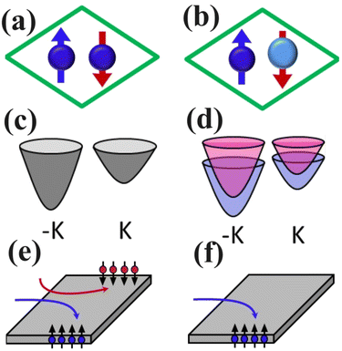
The isovalent alloying assisted AVHE in a hexagonal AFM monolayer is schematically illustrated in Fig. 1. Fig. 1(a) shows that the two magnetic atoms of a hexagonal AFM monolayer per unit cell are the same 3d elements, and its energy extrema of conduction/valence bands is at a high symmetry −K/K point. We assume that the lattice of the hexagonal AFM monolayer has spatial inversion symmetry, but the AFM ordering leads to the simultaneously broken inversion (P) symmetry and time reversal (T) symmetry, which produce spontaneous valley polarization (Fig. 1(c)). However, the system possesses PT symmetry, which gives rise to spin degeneracy, prohibiting the realization of the AVHE. PT symmetry is an antiunitary symmetry, which leads to (PT)2= −1. Under PT symmetry, arbitrary k is invariant, because both P and T map k to −k. For a system with PT symmetry, the Hamiltonian H(k) should meet [H(k), PT] = 0. The energy eigenvalue of an arbitrary eigenstate |ψ(k)〉 of H(k) is E(k), and its PT pair |ϕ(k)〉 = PT|ψ(k)〉 is also an eigenstate with k and E(k). For a PT symmetry system, every band must be doubly degenerate with spin-up and spin-down, even in the presence of SOC (for details, see ref. 29). By breaking the PT symmetry, for example breaking the P symmetry by isovalent alloying, the spin splitting can be achieved.Due to PT symmetry, the zero berry curvature (Ω(k)) everywhere in the momentum space can be observed. However, the Berry curvatures for the spin-up and spin-down channels are nonzero, and they are equal in magnitude and opposite in sign. In the presence of a longitudinal in-plane electric field, an appropriate electron doping produces a valley-spin Hall effect (Fig. 1(e)). For the valley-spin Hall effect, the Berry curvatures make the Bloch carriers of spin-up and spin-down form the same −K valley acquiring opposite anomalous transverse velocity, which leads to the accumulation of spin-up and spin-down carriers at the two edges of the sample, respectively.
Here, substituting elements via isovalent alloying (one of the two magnetic atoms is replaced by a 4d element with the same outer electrons) can be applied to break the PT symmetry (Fig. 1(b)), and the spin degeneracy of −K and K valleys can be removed. Our proposed system can be called an asymmetric AFM semiconductor (AAFMS).30 Although the two magnetic atoms (3d and 4d elements) have the same surrounding atomic arrangement, the energy level of 4d electrons is higher than that of 3d ones (d orbital mismatch), producing spin splitting. Due to the broken PT symmetry, the spin splitting of the −K and K valleys can be observed (Fig. 1(d)), resulting in the AVHE (Fig. 1(f)).
Among bulk materials, the AAFMS property has been predicted in a family of double perovskites A2CrMO6 (A = Ca, Sr, and Ba, and M = Ru, Os).30 The large spin polarization around the Fermi energy level has been observed due to d orbital mismatch among these magnetic ions. Among 2D materials, CrMoA2S6 (A = C, Si, or Ge) monolayers are AAFMSs, of which CrMoC2S6 has the highest Néel temperature of 556 K with robust magnetism against carrier doping and external in-plane strain.31 Next, we take the CrMoC2S6 monolayer as an example to illustrate our proposal.
III. Computational details
We perform spin-polarized first-principles calculations within density functional theory (DFT)32,33 by using the projector augmented-wave (PAW) method, as implemented in the Vienna ab initio Simulation Package (VASP).34–36 We use the generalized gradient approximation of Perdew–Burke–Ernzerhof (PBE-GGA)37 as the exchange–correlation functional. A kinetic energy cutoff of 500 eV, a total energy convergence criterion of 10−8 eV, and a force convergence criterion of 0.0001 eV Å−1 are set to obtain accurate results. To describe the strong correlation interaction of 3d and 4d electrons in CrMoC2S6, a Hubbard correction Ueff = 3.0 eV (ref. 31) is used for the rotationally invariant approach proposed by Dudarev et al.38 The SOC is incorporated for investigation of valley splitting and magnetic anisotropy energy (MAE). To avoid the interaction between adjacent layers, a vacuum space of more than 20 Å along the z direction is adopted. A 12 × 12 × 1 Γ-centered Monkhorst–Pack grid is used to sample the Brillouin zone (BZ). Based on the finite displacement method, the interatomic force constants (IFCs) are calculated by employing a 3 × 3 × 1 supercell, and the phonon dispersion spectrum is obtained using the Phonopy code.39 The elastic stiffness tensors Cij are calculated by using the strain–stress relationship (SSR) method. C2Dij has been renormalized by C2Dij = LzC3Dij, where Lz is the length of the unit cell along the z direction. The Berry curvatures are calculated directly from the calculated wave functions based on Fukui's method,40 as implemented in the VASPBERRY code.41–43IV. Crystal and electronic structures
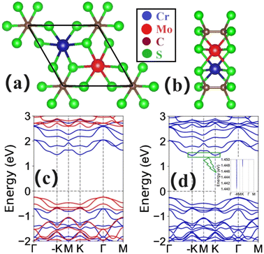
It has been proved that the CrMoC2S6 monolayer possesses dynamical and thermal stabilities, and the experimental possibility is also confirmed by the formation energy.31 Here, we also calculate two independent elastic constants: C11 = 91.69 N m−1 and C12 = 34.57 N m−1, which satisfy the Born criteria of mechanical stability:44C11 > 0 and C11–C12 > 0, confirming its mechanical stability. The crystal structures of CrMoC2S6 are shown in Fig. 2(a) and (b), which crystallizes in the P312 space group (no. 149), lacking spatial inversion symmetry. CrMoC2S6 can be obtained by substituting one Cr of Cr2C2S6 with Mo via isovalent alloying. Cr and Mo are surrounded by six S atoms, forming a honeycomb lattice. Two CS3 moieties are connected by two C atoms, forming a dumbbell-like structure. The optimized equilibrium lattice constants of CrMoC2S6 are a = b = 5.714 Å according to the GGA+U method. To determine the magnetic ground state of CrMoC2S6, the FM and three AFM configurations (AFM1, AFM2 and AFM3) are constructed (Fig. S1, ESI†), and the AFM1 is called the Néel AFM state. The energy of AFM1 per unit cell is 580 meV, 365 meV and 191 meV lower than those of FM, AFM2 and AFM3 cases, respectively, confirming that CrMoC2S6 possesses the AFM1 ground state.The energy band structures of CrMoC2S6 and Cr2C2S6 without SOC are plotted in Fig. 2(c) and Fig. S2 (ESI†), respectively. The lattice of Cr2C2S6 has spatial inversion symmetry, but the inversion symmetry will disappear with AFM1 ordering. However, a combination of inversion symmetry P and time-reversal symmetry T (PT) exist, which leads to disappeared spin splitting. For CrMoC2S6, a large spin splitting around the Fermi energy level can be observed. The symmetry of spin splitting of CrMoC2S6 is s-wave, which is different from the symmetry of spin splitting of altermagnetism,45,46i.e., d-wave, g-wave or i-wave. In other words, the altermagnets exhibit momentum-dependent spin splitting, while a spin splitting occurs throughout the whole BZ for CrMoC2S6. The total magnetic moment of the system is equal to the number of spin-up electrons minus the number of spin-down electrons. For CrMoC2S6, both spin channels have energy band gaps, so the numbers of electrons of both spin channels are integers. Therefore, the total magnetic moment of CrMoC2S6 per unit cell is strictly equal to 0μB and does not deviate from 0μB slightly. Strictly speaking, this CrMoC2S6 should be called a fully compensated ferrimagnet. For altermagnetism, the absolute values of the magnetic moments of two magnetic atoms with opposite spins are strictly equal because they are connected together by rotational symmetry.45,46 For our discussed case CrMoC2S6, the absolute values of the magnetic moments of two magnetic atoms with opposite spins are not strictly equal because they are not symmetrically connected. It is clearly seen that CrMoC2S6 is an indirect gap semiconductor with a conduction band bottom (CBM)/valence band maximum (VBM) at the K/Γ point, and the energies of −K and K valleys in the conduction bands are degenerate. Monolayer CrMoC2S6 is a bipolar AFM semiconductor with the VBM and CBM in different spin channels.
When including SOC, the magnetic orientation of CrMoC2S6 should be determined by MAE, and only the out-of-plane case can produce spontaneous valley polarization.27 The MAE can be calculated using EMAE = E‖SOC − E⊥SOC, where ‖ and ⊥ mean that spins lie in the plane and out-of-plane. The positive MAE means out-of-plane magnetic anisotropy, while the negative value indicates in-plane one. The predicted MAE is 148 meV per unit cell, which means the out-of-plane easy magnetization axis of CrMoC2S6. The energy band structures of CrMoC2S6 with SOC are plotted in Fig. 2(d), which shows the valley polarization with the valley splitting of only 7.4 meV (ΔEC = ECK − EC−K), and the energy of the K valley is higher than that of the −K valley. In order to strengthen valley splitting, strain engineering may be an effective and feasible method.47 In the next section, we will study the strain effects on the magnetic and electronic properties of CrMoC2S6.
V. Strain effects
Here, a/a0 (0.94–1.06) is used to simulate the biaxial strain, where a and a0 are the strained and unstrained lattice constants, respectively. a/a0 < 1/> 1 means the compressive/tensile strain. Firstly, we determine the magnetic ground state of strained CrMoC2S6 by the energy difference between FM/AFM2/AFM3 and AFM1 configurations, which is shown in Fig. 3(a). Within the considered a/a0 range, the AFM1 ordering is always the ground state. With increasing strain, the strength of the magnetic interaction is reduced. To maintain spontaneous valley polarization, the direction of magnetization is another key factor. The MAE vs. a/a0 is plotted in Fig. 3(b), which shows a transition of the magnetization direction. Compressive strain can make the magnetization direction of CrMoC2S6 change from the out-of-plane case to the in-plane case, and this critical strain point is about 0.98. Fortunately, tensile strain can enhance the MAE of CrMoC2S6, thereby promoting the spontaneous valley polarization.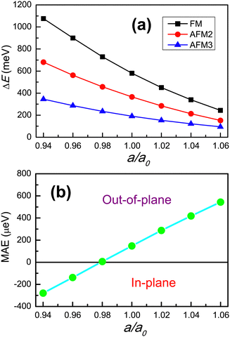 | ||
| Fig. 3 For CrMoC2S6, (a) the energy difference between FM/AFM2/AFM3 and AFM1 orderings as a function of a/a0; (b) the MAE vs. a/a0. | ||
The energy band structures of CrMoC2S6 at representative a/a0 by using both GGA and GGA + SOC are plotted in Fig. S3 (ESI†), and the enlarged figures of SOC energy band structures near the Fermi energy level for the conduction band are plotted in Fig. 4. The valley splitting with assumed out-of-plane and intrinsic magnetization directions for the conduction band as a function of a/a0 is plotted in Fig. 5. Based on Fig. S3 (ESI†), CrMoC2S6 is always a bipolar AFM semiconductor. Near the Fermi energy level, the conduction bands come from the spin-up channel, while the valence band is dominated by the spin-down channel. With assumed out-of-plane magnetization, the compressive strain can induce K valley polarization, while the tensile strain maintains −K valley polarization. Both increasing compressive and tensile strains can enhance the absolute size of valley splitting |ΔEC|. From this perspective, strain can be considered analogous to a pseudomagnetic field. Stain-driven valley polarization transition can also be observed in the Janus GdClF monolayer.48 When considering intrinsic magnetic anisotropy, the spontaneous valley polarization appears with a/a0 being larger than 0.98. At a/a0 = 1.06, the corresponding valley splitting is about 19.5 meV.
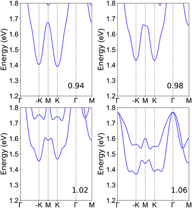 | ||
| Fig. 4 For CrMoC2S6, the energy band structures of conduction bands near the Fermi energy level with SOC at representative a/a0 (0.94, 0.98, 1.02, and 1.06). | ||
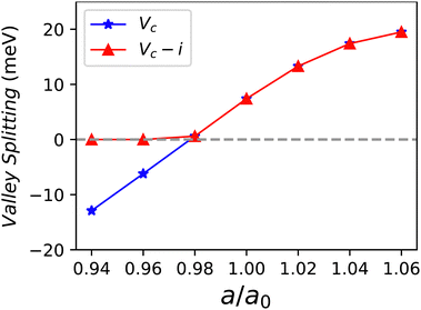 | ||
| Fig. 5 For CrMoC2S6, the valley splitting with assumed out-of-plane and intrinsic magnetization directions (Vc and Vc–i) for the conduction band as a function of a/a0. | ||
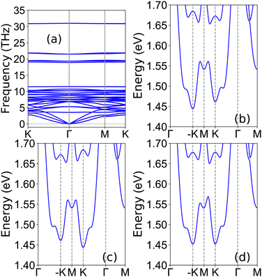
Finally, taking typical a/a0 = 1.04, the physical properties of CrMoC2S6 are detailedly investigated. The calculated phonon spectrum of CrMoC2S6 with a/a0 = 1.04 is shown in Fig. 6(a), which shows no obvious imaginary frequencies, indicating its dynamic stability. The energy band structures of conduction bands near the Fermi energy level with SOC for the magnetization direction along the positive z, negative z, and positive x directions are plotted in Fig. 6 (b)–(d). Fig. 6(b) shows the valley polarization with a valley splitting of 17.4 meV, and the energy of the K valley is higher than that of the −K valley. Fig. 6(c) indicates that the valley polarization can be switched by reversing the magnetization direction. When the magnetization direction of CrMoC2S6 is in-plane (see Fig. 6(d)), no valley polarization can be observed.
For CrMoC2S6 at a/a0 = 1.04, the distributions of Berry curvatures of total, spin-up and spin-down are plotted in Fig. 7. For purposes of comparison, the related distribution of the Berry curvatures of Cr2C2S6 is also shown in Fig. S4 (ESI†). Due to PT symmetry, the total Berry curvatures of Cr2C2S6 are zero, but the berry curvatures are opposite for the same valley at different spin channels and different valleys at the same spin channel. However, for CrMoC2S6, the total Berry curvatures are nonzero at −K and K valleys due to the broken PT symmetry. The Berry curvatures of the −K and K valleys have opposite signs for the same spin channel, and the Berry curvatures are also opposite for the same valley at different spin channels. With an applied longitudinal in-plane electric field, the Bloch carriers will acquire an anomalous transverse velocity v⊥ ∼ E‖ × Ω(k).4 When the Fermi energy level is shifted between the −K and K valleys in the conduction band, the spin-up carriers from the −K valley will accumulate along one edge of the sample, resulting in the AVHE (Fig. 1(f)).
 | ||
| Fig. 7 For CrMoC2S6 with a/a0 = 1.04, the distribution of Berry curvatures of total (a), spin-up (b) and spin-down (c). | ||
In general, 3d electrons have a stronger electron correlation than 4d electrons. For monolayer CrMoC2S6 at a/a0 = 1.04, the different U (Cr, Mo) values are also considered to confirm the reliability of our results. From U (3, 2) to U (3, 3) to U (4, 3), the magnetic interaction energy and MAE of CrMoC2S6 become weak, but it always possesses out-of-plane AFM1 ordering. At different U (Cr, Mo) values, the energy band structures of conduction bands near the Fermi energy level with SOC for the magnetization direction along the positive z direction are plotted in Fig. S5 (ESI†). They all show −K valley polarization, and the valley splitting increases with increasing U (Cr, Mo). The related data are summarized in Table 1.
| U (Cr, Mo) | E FM | E AFM1 | E AFM2 | E AFM3 | MAE | V c |
|---|---|---|---|---|---|---|
| (3, 2) | 371 | 0 | 231 | 128 | 478 | 16.5 |
| (3, 3) | 339 | 0 | 214 | 122 | 419 | 17.4 |
| (4, 3) | 292 | 0 | 181 | 107 | 416 | 18.2 |
To elucidate the mechanical performance of CrMoC2S6, an isotropic in-plane Young's modulus C2D of 78.66 N m−1 is predicted. This is weaker than those of graphene (∼340 ± 40 N m−1) and MoS2 (∼126.2 N m−1),49,50 indicating the better mechanical flexibility of monolayer CrMoC2S6, which is in favour of experimentally enhancing valley splitting by strain. For the MoS2 monolayer, the strain with as large as 5.6% has been achieved experimentally.51 Therefore, 1.04 (4%) strain in CrMoC2S6 can be realized experimentally due to small C2D.
VI. Conclusion
In summary, we present a way to induce the AVHE in a hexagonal AFM monolayer by isovalent alloying. Using first-principles calculations, we confirm the validity of our proposed way by an extensive study of the CrMoC2S6 monolayer. Due to broken P and T symmetries in CrMoC2S6, there is a spontaneous valley polarization. Moreover, the spin splitting can occur due to broken PT symmetry, which can also be explained by the d orbital mismatch of different magnetic atoms. Strain engineering can be used to tune valley splitting, and the calculated results show that tensile strain can enhance the valley splitting of CrMoC2S6 with the out-of-plane AFM1 ordering. With an applied longitudinal in-plane electric field, the Berry curvature can produce the AVHE. Our work is expected to speed up the realization of the AVHE in AFM monolayers, and provide a route for constructing energy-efficient and ultrafast valleytronic devices.Data availability
The magnetic configurations and the related energy band structures and Berry curvature distributions have been included as part of the ESI.†Conflicts of interest
There are no conflicts to declare.Acknowledgements
This work is supported by the Natural Science Basis Research Plan in Shaanxi Province of China (2021JM-456). We are grateful to Shanxi Supercomputing Center of China, and the calculations were performed on TianHe-2.References
- J. R. Schaibley, H. Yu, G. Clark, P. Rivera, J. S. Ross, K. L. Seyler, W. Yao and X. Xu, Nat. Rev. Mater., 2016, 1, 16055 CrossRef CAS.
- G. Pacchioni, Nat. Rev. Mater., 2020, 5, 480 CrossRef CAS.
- S. A. Vitale, D. Nezich, J. O. Varghese, P. Kim, N. Gedik, P. Jarillo-Herrero, D. Xiao and M. Rothschild, Small, 2018, 14, 1801483 CrossRef PubMed.
- D. Xiao, M. C. Chang and Q. Niu, Rev. Mod. Phys., 2010, 82, 1959 CrossRef CAS.
- A. Srivastava, M. Sidler, A. V. Allain, D. S. Lembke, A. Kis and A. Imamoglu, Nat. Phys., 2015, 11, 141 Search PubMed.
- K. F. Mak, K. He, J. Shan and T. F. Heinz, Nat. Nanotechnol., 2012, 7, 494 CrossRef CAS.
- H. Zeng, J. Dai, W. Yao, D. Xiao and X. Cui, Nat. Nanotechnol., 2012, 7, 490 CrossRef CAS.
- M. Zeng, Y. Xiao, J. Liu, K. Yang and L. Fu, Chem. Rev., 2018, 118, 6236 CrossRef CAS PubMed.
- C. Zhao, T. Norden, P. Zhang, P. Zhao, Y. Cheng, F. Sun, J. P. Parry, P. Taheri, J. Wang, Y. Yang, T. Scrace, K. Kang, S. Yang, G. Miao, R. Sabirianov, G. Kioseoglou, W. Huang, A. Petrou and H. Zeng, Nat. Nanotechnol., 2017, 12, 757 CrossRef CAS PubMed.
- D. MacNeill, C. Heikes, K. F. Mak, Z. Anderson, A. Kormanyos, V. Zolyomi, J. Park and D. C. Ralph, Phys. Rev. Lett., 2015, 114, 037401 CrossRef CAS PubMed.
- X. X. Zhang, Y. Lai, E. Dohner, S. Moon, T. Taniguchi, K. Watanabe, D. Smirnov and T. F. Heinz, Phys. Rev. Lett., 2019, 122, 127401 CrossRef CAS.
- T. Cao, G. Wang, W. Han, H. Ye, C. Zhu, J. Shi, Q. Niu, P. Tan, E. Wang, B. Liu and J. Feng, Nat. Commun., 2012, 3, 887 CrossRef.
- W. Y. Tong, S. J. Gong, X. Wan and C. G. Duan, Nat. Commun., 2016, 7, 13612 CrossRef CAS.
- Y. B. Liu, T. Zhang, K. Y. Dou, W. H. Du, R. Peng, Y. Dai, B. B. Huang and Y. D. Ma, J. Phys. Chem. Lett., 2021, 12, 8341 CrossRef CAS.
- Z. Song, X. Sun, J. Zheng, F. Pan, Y. Hou, M.-H. Yung, J. Yang and J. Lu, Nanoscale, 2018, 10, 13986 RSC.
- J. Zhou, Y. P. Feng and L. Shen, Phys. Rev. B, 2020, 102, 180407 CrossRef CAS.
- P. Zhao, Y. Ma, C. Lei, H. Wang, B. Huang and Y. Dai, Appl. Phys. Lett., 2019, 115, 261605 CrossRef.
- X. Y. Feng, X. L. Xu, Z. L. He, R. Peng, Y. Dai, B. B. Huang and Y. D. Ma, Phys. Rev. B, 2021, 104, 075421 CrossRef CAS.
- Y. Zang, Y. Ma, R. Peng, H. Wang, B. Huang and Y. Dai, Nano Res., 2021, 14, 834 CrossRef CAS.
- R. Peng, Y. Ma, X. Xu, Z. He, B. Huang and Y. Dai, Phys. Rev. B, 2020, 102, 035412 CrossRef CAS.
- W. Du, Y. Ma, R. Peng, H. Wang, B. Huang and Y. Dai, J. Mater. Chem. C, 2020, 8, 13220 RSC.
- R. Li, J. W. Jiang, W. B. Mi and H. L. Bai, Nanoscale, 2021, 13, 14807 RSC.
- T. Jungwirth, J. Sinova, A. Manchon, X. Marti, J. Wunderlich and C. Felser, Nat. Phys., 2018, 14, 200 Search PubMed.
- T. Zhao, S. Xing, J. Zhou, N. Miao and Z. Sun, J. Mater., 2024, 10, 269 Search PubMed.
- W. Du, R. Peng, Z. He, Y. Dai, B. Huang and Y. Ma, npj 2D Mater. Appl., 2022, 6, 11 Search PubMed.
- Y. Xu, H. Liu, Y. Dai, B. Huang and W. Wei, Appl. Phys. Lett., 2023, 122, 242404 CrossRef CAS.
- S. D. Guo, Y. L. Tao, Z. Y. Zhuo, G. Zhu and Y. S. Ang, Phys. Rev. B, 2024, 109, 134402 CrossRef CAS.
- S. D. Guo, W. Xu, Y. Xue, G. Zhu and Y. S. Ang, Phys. Rev. B, 2024, 109, 134426 CrossRef CAS.
- Y. Xue, W. Xu, B. Zhao, J. Zhang and Z. Yang, Phys. Rev. B, 2023, 108, 075138 CrossRef CAS.
- X. Li, X. Wu, Z. Li and J. Yang, Phys. Rev. B: Condens. Matter Mater. Phys., 2015, 92, 125202 CrossRef.
- P. Wang, D. X. Wu, K. Zhang and X. J. Wu, J. Phys. Chem. Lett., 2022, 13, 3850 CrossRef CAS.
- P. Hohenberg and W. Kohn, Phys. Rev., 1964, 136, B864 CrossRef.
- W. Kohn and L. J. Sham, Phys. Rev., 1965, 140, A1133 CrossRef.
- G. Kresse, J. Non-Cryst. Solids, 1995, 193, 222 CrossRef.
- G. Kresse and J. Furthmuller, Comput. Mater. Sci., 1996, 6, 15 CrossRef CAS.
- G. Kresse and D. Joubert, Phys. Rev. B: Condens. Matter Mater. Phys., 1999, 59, 1758 CrossRef CAS.
- J. P. Perdew, K. Burke and M. Ernzerhof, Phys. Rev. Lett., 1996, 77, 3865 CrossRef CAS PubMed.
- S. L. Dudarev, G. A. Botton, S. Y. Savrasov, C. J. Humphreys and A. P. Sutton, Phys. Rev. B: Condens. Matter Mater. Phys., 1998, 57, 1505 CrossRef CAS.
- A. Togo, F. Oba and I. Tanaka, Phys. Rev. B: Condens. Matter Mater. Phys., 2008, 78, 134106 CrossRef.
- T. Fukui, Y. Hatsugai and H. Suzuki, J. Phys. Soc. Jpn., 2005, 74, 1674 CrossRef CAS.
- H. J. Kim, 2018, https://github.com/Infant83/VASPBERRY.
- H. J. Kim, C. Li, J. Feng, J.-H. Cho and Z. Zhang, Phys. Rev. B, 2016, 93, 041404 CrossRef.
- S. W. Kim, H. J. Kim, S. Cheon and T. H. Kim, Phys. Rev. Lett., 2022, 128, 046401 CrossRef CAS.
- R. C. Andrew, R. E. Mapasha, A. M. Ukpong and N. Chetty, Phys. Rev. B, 2012, 85, 125428 CrossRef.
- L. Smejkal, J. Sinova and T. Jungwirth, Phys. Rev. X, 2022, 12, 031042 CAS.
- I. Mazin, Phys. Rev. X, 2022, 12, 040002 CAS.
- H. X. Cheng, J. Zhou, W. Ji, Y. N. Zhang and Y. P. Feng, Phys. Rev. B, 2021, 103, 125121 CrossRef CAS.
- S. D. Guo, X. S. Guo, X. X. Cai and B. G. Liu, Phys. Chem. Chem. Phys., 2022, 24, 715 RSC.
- K. N. Duerloo, M. T. Ong and E. J. Reed, J. Phys. Chem. Lett., 2012, 3, 2871 CrossRef CAS.
- C. Lee, X. g Wei, J. W. Kysar and J. Hone, Science, 2008, 321, 385 CrossRef CAS.
- D. Lloyd, X. H. Liu and J. W. Christopher, et al. , Nano Lett., 2016, 16, 5836 CrossRef CAS PubMed.
Footnote |
| † Electronic supplementary information (ESI) available. See DOI: https://doi.org/10.1039/d4tc03700f |
| This journal is © The Royal Society of Chemistry 2025 |

