
 Open Access Article
 This Open Access Article is licensed under a
 Creative Commons Attribution 3.0 Unported Licence
Interface energies of Ga2O3 phases with the sapphire substrate and the phase-locked epitaxy of metastable structures explained†
Ilaria
Bertoni
 *,
Aldo
Ugolotti
,
Emilio
Scalise
,
Roberto
Bergamaschini
and
Leo
Miglio
*,
Aldo
Ugolotti
,
Emilio
Scalise
,
Roberto
Bergamaschini
and
Leo
Miglio
Department of Materials Science, University of Milano-Bicocca, via Cozzi 55, 20125 Milan, Italy
First published on 15th November 2024
Abstract
Despite the extensive work carried out on the epitaxial growth of Ga2O3, a fundamental understanding of the nucleation of its different metastable phases is still lacking. Here we address the role of interface energies using density functional theory calculations of α, β and κ-Ga2O3 on (0001) Al2O3 substrates, and different Ga2O3 interlayers. In conjunction with surface energies and misfit strain contributions, we demonstrate that α-Ga2O3 is the preferred phase in 2D islands, when the low growth temperatures and the high growth rates hinder 3D island nucleation. This quantitatively explains the phase-locking in mist-CVD experiments.
Introduction
The monoclinic phase of gallium oxide (β-Ga2O3) has positioned itself as a strong contender in next-generation high-power electronics,1–3 due to some superior properties compared to the current leader, silicon carbide (4H-SiC). These advantages include a wider energy bandgap (4.9 eV), providing a higher breakdown voltage, and moderate epitaxial growth temperatures, 700–800 °C, by metal–organic chemical vapor deposition (MOCVD), potentially enabling integration into the Si technology. However, while β-Ga2O3 is the stable crystal phase, epitaxial growth can yield different competing phases. Among these, the α phase (rhombohedral) and the κ phase (orthorhombic, previously addressed as ε-hexagonal) are particularly attractive for power electronics.4,5 Understanding and controlling the growth of different Ga2O3 phases is crucial to unlock their full potential for high-power device fabrication.c-Sapphire emerges as the preferred substrate for growing Ga2O3 phases via heteroepitaxy, both due to its structural coherence with α-Ga2O3 and its convenient cost compared to other potential substrates. The α phase grows exposing the same surface as that of the substrate, i.e. the (0001) plane. The monoclinic β phase and the orthorhombic κ phase grow in three-fold rotational domains,4 due to the peculiar arrangement of the oxygen atoms in layers along the (![[2 with combining macron]](https://www.rsc.org/images/entities/char_0032_0304.gif) 01) plane of the former and the (001) plane of the latter,6–11 which nearly matches in symmetry the triangular oxygen network of c-sapphire.
01) plane of the former and the (001) plane of the latter,6–11 which nearly matches in symmetry the triangular oxygen network of c-sapphire.
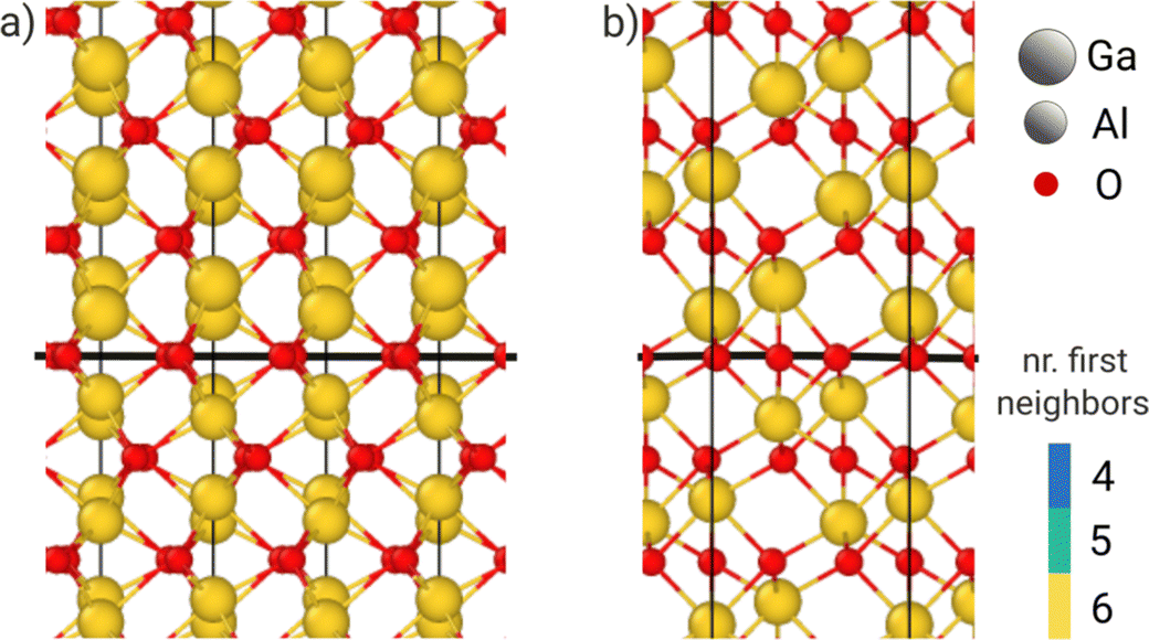
As shown in Fig. 1, the three phases are characterized by a different Ga–O coordination. While in α-Ga2O3 all Ga atoms are coordinated with six O atoms forming octahedral cages, in β and κ phases 50% and 25% of Ga atoms are four-fold coordinated, respectively, forming tetrahedral complexes. It is worth pointing out that in the κ phase one third of Ga atoms in the octahedral cage may result in five-fold coordination, depending on the coordination cut-off radius, as one oxygen atom is 0.45 Å more distant than the others, due to the distortion of the octahedral cage (see the ESI† of our previous paper on Ga2O3 surfaces12). The vertical axis in Fig. 1 indicates the actual growth direction and the alternate stacking of oxygen atom layers (in red) is evident. Moreover, all Ga2O3 phases experience a degree of mismatch with the sapphire lattice. This mismatch ranges from about 4% for α-Ga2O3 to a larger and anisotropic mismatch for β and κ phases.12 The mismatch creates strain at the interface between the Ga2O3 film and the sapphire substrate. Different mechanisms, such as misfit dislocations (especially for α-Ga2O3) and defected boundaries between rotational domains (especially for the β phase), may be responsible for strain release, without considering elastic relaxation in three-dimensional islands.6,13 At the moment, very little is experimentally assessed in terms of such strain relief.
 | ||
| Fig. 1 Optimized structures of the conventional cell of bulk α- (a), β- (b) and κ- (c) Ga2O3. Ga and O atoms are shown with grey and red spheres, respectively. Tetrahedral, pentahedral and octahedral Ga–O coordination structures are shown through yellow, green and blue surfaces. The vertical direction of the image is aligned with the growth direction of Ga2O3 on the c-sapphire substrate. For each phase the inequivalent epitaxial layer is indicated by h. | ||
The role of the interface and its related kinetic issues appears to be evident by the fact that various growth methods (mist-CVD, MOCVD, high-vacuum VPE, MBE, PLD, and halide-VPE) and diverse growth conditions14–18 lead to different phases. In this complex picture, some trends are sufficiently clear: low temperatures (and/or high growth rates) favor the α phase, intermediate temperature values and/or rates may favour the κ phase, whereas conditions closer to equilibrium induce the stable β phase. In a recent review by Kaneko et al.,17 primarily focusing on the investigation of low temperature mist-CVD growth of α-Ga2O3, the authors suggest how the single “mist” precursor, a gallium acetylacetonate complex, approaches the surface and anchors to a surface hydroxyl by hydrogen bonding at the water-covered surface, producing the on-site deposition of Ga with no surface diffusion. It is the lack of long surface mean free paths that promotes a purely two-dimensional growth, in turn enhancing the role of interface energies and producing what is called a metastable phase-locking. This latter phenomenon is common in other deposition techniques when low growth temperatures and high deposition rates are achieved. Such a mechanism would kinetically favour the phases with a better structural match with the substrate, independent of other thermodynamic factors that come into play with temperature (and surface diffusion length).
However, quantitative validation of this intuition was not possible due to the lack of interface energies. Therefore, the ultimate goal of our work is to provide interface energies for a deeper understanding of the stabilization of the different Ga2O3 phases on sapphire and Ga2O3 interlayers, at the same time providing a solid framework for growth models to be explored, at least for what concerns the very early growth stages.
When growing epitaxially on a substrate, the key factors involved in the stabilization of the film include its cohesion energy, which is also affected by the strain induced by the lattice mismatch with the substrate, the interface energy, resulting from the chemical bonds formed between the film and the substrate, and the surface energy of the growing front exposed by the film (with or without strain). These are particularly relevant for a 2D island growth mode, in addition to a perimetral step energy that is really unknown in detail and can be taken to be eventually negligible for large surface covering. The phase-locking is generated by a strong coherent or commensurate matching to the substrate, an issue which is mostly active when the growth proceeds layer by layer, i.e. by 2D islands, as thick as one O–Ga bi-layer in α-Ga2O3, two bi-layers in β- or κ-Ga2O3 (see Fig. 1). The islands are actually taken as “infinitely wide” 2D layers, as we consider a later stage of growth. In contrast, in the case of 3D β island growth, the surface energy contribution of all exposed facets as well as the actual strain relaxation provided by the peculiar island shape should play a major role.
In a recent paper,12 we presented a comparison of volume and surface energies for α, β, and κ phases of Ga2O3, as calculated by density functional theory (DFT). We also accounted for the strain produced by the substrate and how it affects such results. For each phase, the elastic contribution of the lattice misfit with the sapphire substrate was calculated by imposing the matching between the planar network of oxygen atoms of the film and that of the substrate. Moreover, the elastic contribution of the lattice misfit with a plastically relaxed α-Ga2O3 buffer layer was considered. In fact, surveying the literature, one notices that Ga2O3 phases can nucleate directly on the substrate or on a α-Ga2O3 interlayer, both relaxed or fully strained by a coherent interface with sapphire.19 The quantity missing in our previous work was the interface contribution that is the main topic of the present work. In ref. 20 a thick film of κ-Ga2O3 is shown to grow on β-Ga2O3, possibly with some strain, then we also include the study of this interface in our work.
Here we demonstrate that the structural similarity between the film and the substrate (briefly, in terms of the percentage of octahedral and tetrahedral cages of O with respect to the fully octahedral structure of α-sapphire) is the leading criterion in lowering the interface energies and explains the quantitative meaning of the metastable phase-locking, especially the α phase in mist-CVD.
Finally, we address the following question: is the strain relaxation by dislocation nucleation in the α phase disrupting the kinetic phase locking, or is it the nucleation and growth of 3D islands, as produced by higher temperatures and lower growth rates? By mist-CVD we know that the α phase grows continuously in fully relaxed films.13 Still, by MBE or MOCVD at different temperatures and rates, the β phase eventually appears. Therefore, we draw a simple nucleation model of the three phases considering 2D islands on sapphire, strained α or relaxed α. The subsequent discussion sheds some light on the experimental issues and provides some indications for future deposition tests.
Methods
Interface energy calculations
All the DFT calculations were performed using the VASP software.21–23 We chose the Perdew–Burke–Ernzerhof exchange–correlation functional revised for solids (PBEsol),24 maintaining continuity with our previous work on surface energies.12 We employed pseudo-potentials with 6 and 13 electrons in the valence states for O and Ga atoms, respectively. We optimized the atomic coordinates and the lattice parameters of all bulk structures, including the one of α-Al2O3, using a plane-waves cutoff of 850 eV. All the resulting lattice parameters are reported in Table S1 (ESI†). Then, the following calculations, which do not require the optimization of lattice parameters, were performed with a reduced cutoff of 500 eV, in order to reduce the computational load. The Brillouin zone was sampled through (6 × 6 × 3), (2 × 12 × 6) and (7 × 4 × 4) unshifted Monkhorst–Pack k-point meshes for the α, β and κ cells, respectively. We constructed the substrate slab by aligning its z axis with the c axis of sapphire. Therefore, the hexagonal in-plane lattice of the c-sapphire cell was our reference, with [100]/[120] directions along the x/y axes.The schematics on how the hetero-interfaces were modeled are represented in Fig. 2: the slab of each film (i.e. α-, β- and κ-Ga2O3) was stacked on the ones of different substrates: α-Al2O3 and a fully strained/relaxed α-Ga2O3 buffer layer. We also considered a strained/relaxed interlayer of β-Ga2O3 in the case of the κ film. This was done in a way that, again, the film and the substrate share the layer of oxygen atoms at the interface. The slabs of the film were built in order to align the β [102] along the α [100], the β [010] along the α [120], the κ [100] along the α [100] and the κ [010] along the α [120]. When considering the interface between κ and β phases, the κ [100] is aligned along the β [102] and the κ [010] along the β [010]. Both slabs of the Ga2O3 films and substrate were constructed in a way to expose one free surface, with surface structures corresponding to those investigated in our previous work.12 In order to prevent interactions between periodic replicas of each interface slab along its z-direction, we inserted a vacuum region of 13 Å. The interface slabs were built adapting the in-plane (super)cell parameters of the film to those of the substrate. Thus, considering the epitaxial relationships between the film and the substrate, supercells replicating the slab unit cells of the film or substrate were exploited. The sizes of the supercells and the corresponding misfit strain applied to the film, for each interface, are detailed in Table S2 (ESI†). Finally, to obtain the relaxed interface structure, we optimized the atomic coordinates only, keeping the supercell fixed by the lattice constraints of the substrate. This approach allows a proper release of the stress along the z direction throughout the structural optimization.
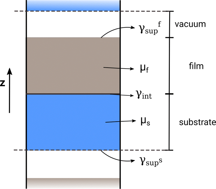 | ||
| Fig. 2 Schematics of the interface slab model: the film (gray) is stacked on top of the substrate (blue). The simulation cell is periodic in x, y and z directions. | ||
As evident in Fig. 1, all oriented Ga2O3 phases can be considered as a stacking of bi-layers (a cation layer and an oxygen layer). When building the corresponding individual slabs, we converged the calculated interface energies with respect to the film and substrate thickness. Hence, when building the interface, we stacked slabs with 7 α-Ga2O3, 9 β-Ga2O3 or 13 κ-Ga2O3 layers of Ga and O atoms (that we call bi-layers) on 7 α-Al2O3 bi-layers. Nonetheless, not all bi-layers are equivalent, since not all the planes show the same arrangement of Ga atoms with the same coordination (taking 2.4 Å as cutoff for the first-neighbors distance). We then define the epitaxial layer as the unit that can be stacked to correctly generate a bulk. We mark the epitaxial layers in each phase as shown in Fig. 1.
We calculated the interface energy as
 | (1) |
Results and discussion
Interface energies
To provide additional insight into the understanding of the epitaxial growth mechanism of different Ga2O3 phases on c-sapphire, we calculated such interface energies γint. Since some experimental works indicate the presence of an intermediate Ga2O3 layer of a different phase, which can be an α interlayer, coherent19 or relaxed,10 for the β phase and for the κ phase,8 or a β interlayer for the κ phase,20 we also calculated γint in these cases. In high-resolution TEM images of Ga2O3 polymorphs on sapphire the alternation of layers of anion and cation across the interfaces is observed.19,20,25 Therefore, for the sake of simplicity, our calculations were focused on sharp interfaces only, i.e. with no intermixing of cation species across the interface. Indeed, such an assumption may constitute a simplification of the actual interfaces,26 but allows us to provide a more comprehensible interpretation of the physical effects that affect the stabilization of the interface. Finally, despite the fact that rotational domains of 120° are known to occur for both β and κ films on sapphire, we calculated interface energies for just one (equivalent) domain orientation, as it is still not understood whether some strain release can be introduced at domain boundaries.All interfaces are constructed in a way that a plane of oxygen atoms is shared between the film and substrate. This, as previously mentioned, is the most intuitive way to build the interface, as both all oriented Ga2O3 phases and c-sapphire present oxygen layers with the same hexagonal symmetry. The structure of the stacked bi-layers is identical in the case of α-Ga2O3 on sapphire (but for an in-plane shift); therefore, only one possible termination can be found matching the position of O atoms at the interface. In contrast, both in β and κ bulk cells two different bi-layers are alternated (see Fig. 1b and c). Each of them has a different alternation of octahedral (or pentahedral) and tetrahedral Ga atoms, leading to either two or four different types of interfaces. Indeed, β phase's termination with sapphire can display either octahedral or tetrahedral Ga atoms only, while κ phase's termination can display either octahedrally coordinated Ga atoms only or both tetrahedrally and pentahedrally coordinated ones. In Table 1 we collect only the interface configurations that lead to the lowest energies. In the case of β and κ films on sapphire, the additional results calculated with other terminations are collected in Fig. S1 and S2 (ESI†). In the case of β on κ interface, out of the four possible interfaces provided by the different combinations of β and κ phase terminations, we considered only the promising one (i.e. with Ga atoms octahedrally coordinated) based on the results obtained for Ga2O3 interfaces with sapphire.
| Film | α-Al2O3 | α-Ga2O3 | α-Ga2Oε3 | β-Ga2O3 | β-Ga2Oε3 |
|---|---|---|---|---|---|
| α-Ga2O3 | −3 | — | — | — | — |
| β-Ga2O3 | 53 | 47 | 52 | — | — |
| κ-Ga2O3 | 27 | 32 | 30 | 21 | 15 |
Generally speaking, these values of γint are sensibly lower than the surface energies,12 as expected. Still, as in the case of the surface energies, it is quite useful to interpret our data by performing an analysis of the optimized configurations through the number of first neighbors of Ga atoms, assuming a cut-off distance of 2.4 Å.
In the case of α-Ga2O3, the interface with α-Al2O3, reported in Fig. 3, is almost homogeneous, as the two slabs have the same structure. No distortion is found nor deviation from the ideal six-fold coordination of the cations: therefore, the corresponding interface behaves almost as a continuation of the bulk. In fact, the calculated interface energy turns out to be −3 meV Å−2 and can be considered negligible, within the precision of our calculation method.
 | ||
| Fig. 3 Front (a) and side (b) view of the α-Ga2O3/α-Al2O3 interface. The black line marks the plane of O atoms shared by both film and substrate. | ||
In contrast, some change in coordination is expected for β-Ga2O3, when forming the interface with sapphire, as the interface energy is much higher. In fact, each tetrahetrally coordinated Ga atom belonging to the second row above the interface gains one additional O neighbor each (see the black arrows in Fig. 4). This change is related to how the Ga and O atoms settle in the first two rows above the interface. The structural and energetic optimization appears not to be affected by the strain, nor by the atomic species of the cation in the substrate, as the same change in coordination is found for the strained and the fully relaxed α-Ga2O3 interlayer as well (see in Fig. S3 and S4, ESI†). Hence, the difference in the structural environment for cations at the interface leads to a sizeable interface energy (as reported in Table 1), that is almost the same for α-Ga2O3 fully strained/relaxed substrate. This trend is confirmed when considering the second interface between the β phase and sapphire (see Fig. S1, ESI†), which displays an array of tetrahedrally coordinated cations at the interface in place of octahedrally coordinated ones: the surface energy is higher (77 meV Å−2) despite the optimization turns most interface cations to a pentahedral coordination.
 | ||
| Fig. 4 Front (a) and side (b) view of the β-Ga2O3/α-Al2O3 interface. The black line marks the plane of O atoms shared by both film and substrate. | ||
When considering the κ-Ga2O3 interface with sapphire, reported in Fig. 5, no change in coordination for cations with respect to their bulk occurs, neither for the substrate nor for the film. It is fair to say that in this case the κ phase displays at the interface a layer of cations already in the octahedral configuration, and the interface energy is actually low, about half the one of β on sapphire. The same structure is found when an α-Ga2O3 buffer layer is present, either strained or fully relaxed (see Fig. S5 and S6, ESI†), and its interface energy is roughly the same as with sapphire. In case the second possible interface with sapphire is considered (see Fig. S2, ESI†), the interface energy raises to 38 meV Å−2, as in this case a layer of cations in tetrahedral and pentahedral coordination is present at the interface, and the structural optimization drives a tendency to turn them to pentahedral and octahedral coordination, respectively.
 | ||
| Fig. 5 Front (a) and side (b) view of the κ-Ga2O3/α-Al2O3 interface. The black line marks the plane of O atoms shared by both the film and the substrate. | ||
Interestingly, the case of an interface between the two most open structures, i.e. κ phase over either a fully strained or a fully relaxed β interlayer (represented in Fig. 6 and Fig. S7, ESI†), results in a very low interface energy. This is the case especially for a strained β phase interlayer. Here, out of the four possible configurations, we are considering the one in which both the film and the substrate display the same coordination for cations at the interface, i.e. in octahedral cages: this is a starting point with a presumable low interface energy, but it further decreases with the structural optimization. This can be explained by the fact that the more open interface allows to turn some more distant cations of the κ phase with octahedral coordination to the fourfold ones, which seems to mimic the β stacking.
 | ||
| Fig. 6 Front (a) and side (b) views of the κ-Ga2O3/β-Ga2O3 interface. β-Ga2O3 interlayer is fully strained on the α-Al2O3 substrate. The black line marks the plane of O atoms shared by both film and substrate. | ||
It is therefore quite evident that out of our result a few clear trends emerge. (1) The structures forming an interface display a lower interface energy if the structures are more similar in the percentage of cations in tetrahedral and octahedral coordination. α-Ga2O3 on sapphire being the lowest in energy, β on sapphire the highest in energy. (2) Particularly, the similarity in structure affects the interface region, so that those configurations preserving a smoother change in coordination are lower in energy, as in the case of interfaces shown in Fig. 2–4 and Fig. S3–S6 (ESI†), with respect to their alternative interface terminations reported in Fig. S1 and S2 (ESI†). (3) The structural optimization is effective in doctoring the change in coordination across the interface, lowering the interface energy, specifically for more open structures, such as β and κ phases.
Energetics of Ga2O3 epitaxial layers and phase-locking
The calculations of interfacial energies from the previous section, combined with the data of surface energy and strain computed in ref. 12 and reported in Table S3 (ESI†), allows for a quantitative evaluation of the relative stability of Ga2O3 epitaxial layers for each phase on either α-Al2O3 or α-Ga2O3 substrates. From classical nucleation theory, the formation energy of a 2D island of phase p can be expressed as a function of the number n of formula units:| ΔGp(n) = −(μgas − μpbulk − Δμpε)n + (γpepi + γpint − γsub)Ap(n) + ΛpLp(n) | (2) |
 , by a coefficient Λp, determined by the actual island shape and by the orientation-dependent, linear energy density of its edges, which are both out of our knowledge.
Since we are interested only in the comparison of the stability between the phases, we conveniently rephrase the eqn (2) to obtain the net energy density (per unit-formula) of a 2D Ga2O3 layer in p phase as
 | (3) |
 . In the latter we include the edge contribution and the reason is two-fold. We assume on statistical grounds that the differences between Ga2O3 islands of different phases are negligible; moreover, we will focus on mature growth stages with large n, hence we deem the perimeter contribution to be less important.
The volumetric and surface contributions calculated for 2D layers of each Ga2O3 phase on either α-Al2O3 and α-Ga2O3, both strained to sapphire lattice parameter and fully relaxed, are reported in Table 2. The resulting ρ2D values are reported as energy levels in Fig. 7.
| Substrate: μbulk | α-Al2O3 | α-Ga2Oε3 | α-Ga2O3 | ||||
|---|---|---|---|---|---|---|---|
| Δμε | (v/h)Δγ | Δμε | (v/h)Δγ | Δμε | (v/h)Δγ | ||
| α-Ga2O3 | 45 | 309 | −553 | 309 | 0 | 0 | 0 |
| β-Ga2O3 | 0 | 540 | −30 | 540 | 207 | 150 | 325 |
| κ-Ga2O3 | 63 | 314 | 0 | 314 | 276 | 10 | 163 |
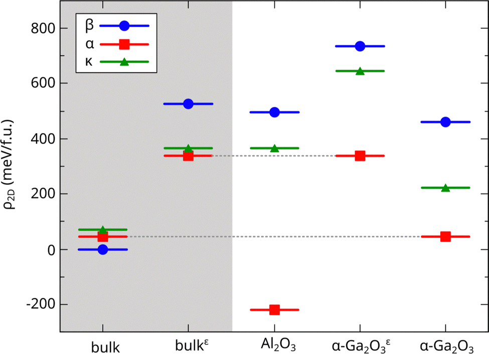 | ||
| Fig. 7 Diagram of ρ2D calculated for 2D films of the Ga2O3 polymorphs, considering different substrates. The bulk values are reported on the left as a reference, also accounting for the misfit strain induced by the Al2O3 substrate (labelled with ε). | ||
While for the bulk phases (relaxed, first column in the gray area) the most stable phase is β-Ga2O3, followed by α and κ, when growing epitaxial layers on α-Al2O3 such ordering is radically changed. Indeed, the lattice mismatch of a single domain with the substrate results in a biaxial strain (ε), generating a substantial increment of the bulk chemical potential as made evident in the second column of Fig. 7, for the infinite bulk correspondingly strained. The effect is more dramatic for the β phase, which becomes strongly unfavorable even against the κ one. In the third column, the surface energy of the sapphire substrate comes in, along with its substitution by the interface energy and the surface energy of the first Ga2O3 epitaxial layer on the substrate. Here, the energy levels of β and κ phases are nearly aligned with the second column, as Δγ ≈ 0. In contrast, for the first epitaxial layer of α-Ga2O3 the surface energy gain from replacing the costly (001) α-Al2O3 (113 meV Å−2) surface with the more convenient (001) α-Ga2O3 (88 meV Å−2), along with the negligible benefit in forming the interface, results in a negative Δγ that largely compensate the elastic energy. This surface/interface advantage is so large that growing the α-Ga2O3 epilayer on α-Al2O3 becomes even more convenient than the formation of the bulk phase.
In the fourth and fifth columns, we find the values for one epitaxial layer on top a coherently strained interlayer of α-Ga2O3, respectively. As adding one epitaxial layer of the α phase on top is like to add one layer inside the (thick) intralayer, the energy values of the former case correctly align to the bulk value with the corresponding strain, while the latter one correctly aligns to the relaxed bulk value (horizontal dashed lines). The hierarchy with respect to the β and κ phase does not change substantially and it is important to say that such a situation eventually corresponds to the additional layers after the very first few ones, either coherent to the substrate, or with a full plastic relaxation of the α phase.
These results explain the phase-locking mechanism proposed by Kaneko17 for the α phase in mist-CVD, because the hierarchy of the stability of different phases of the film mainly follows the structural similarity with the substrate, in addition to the larger misfit strain of the β phase. Therefore, our model supports the epitaxial growth of α-Ga2O3 film first on the bare c-sapphire substrate, either as a thin interfacial layer19 or as a thick film.13
It is fair to say that also the κ phase may result in a few mist-CVD experiments on c-sapphire, either with one ultrathin α interlayer, or directly on sapphire if the mist flow is carefully stabilized,27 but we do not know how the competitive kinetics of plastic relaxation between the α phase and the κ phase acts in producing dislocations,28 an issue not included in our modelling. Anyhow, in Fig. 7 it is clear that the κ phase is the next favorite structure in 2D growth, appearing when for some growth conditions the α phase is hindered. This is apparent in a few HVPE experiments, providing high growth rates because of the Cl catalytic action, where single domain κ layers are grown on sapphire with dislocations,29 or rotational domains appear on c-sapphire with one ultrathin GaN intralayer.30 If we move to MOCVD experiments, usually at higher temperatures, the κ phase appears after an interlayer of α (first) and γ defected phases,25 or with one interlayer of β and γ phases intermixed,20 apparently originated by merged 3D islands. Therefore, it appears that the only way to explain the growth of the β phase straightforwardly on a sapphire substrate, or after an α phase interlayer, is to allow for elastic relaxation by 3D island nucleation, or to some plastic relaxation induced by domain borders, more likely grain boundaries among coalesced 3D islands, or columnar grains. In both cases, higher growth temperatures and reduced growth rates are necessary, in order to allow for larger surface mean free paths. Unfortunately, the morphology of the very early stages of β and κ phase growth and the corresponding strain release have not been characterized so far to a sufficient extent to draw an accurate modelling, including such kinetic effects.
Conclusions
In this work we calculated the interface energies for α, β and κ phases of Ga2O3 on c-sapphire substrate by considering the presence of a shared network of O atoms between film and substrate. We investigated the role of the strain at the interface and we identified the similarity in the percentage of cationcoordination between the two sides of the interface as the major driving force for the lowest energies.Using these values, we then performed a comparison between the relative stability of epitaxial films of the Ga2O3 polymorphs. Our analysis reveals that for a purely 2D growth of Ga2O3 on α-Al2O3 the α phase is the most favorable and remains as such even if considering the nucleation of a new layer on top of an existing, either relaxed or not, α-Ga2O3 interlayer. This provides a quantitative interpretation of the phase-locking effect proposed in ref. 17, corroborating the idea that α-Ga2O3 is preferred in mist-CVD experiments, due to its convenient interaction with the underlying substrate.
Author contributions
I. B. investigation, visualization, writing – original draft; A. U. resources, data curation, writing – reviewing & editing; E. S. validation, methodology, writing – reviewing & editing; R. B. investigation, methodology, writing – reviewing & editing; L. M. conceptualization, funding acquisition, supervision.Data availability
All details to reproduce the calculations are reported in the Methods section of the main manuscript and the files of all the optimized structures are collected in the archive supplementary_information_geometries.zip.Conflicts of interest
There are no conflicts to declare.Acknowledgements
This study was carried out within the MOST-Sustainable Mobility Center and received funding from the European Union Next-GenerationEU (PIANO NAZIONALE DI RIPRESA E RESILIENZA (PNRR)-MISSIONE 4 COMPONENTE 2, INVESTIMENTO 1.4 – D. D. 1033 17/06/2022, CN00000023). We acknowledge the CINECA consortium under the ISCRA initiative for the availability of high-performance computing resources and support.References
- S. J. Pearton, J. Yang, I. Cary, H. Patrick, F. Ren, J. Kim, M. J. Tadjer and M. A. Mastro, Appl. Phys. Rev., 2018, 5, 011301 Search PubMed.
- M. Biswas and H. Nishinaka, APL Mater., 2022, 10, 060701 CrossRef CAS.
- A. J. Green, J. Speck, G. Xing, P. Moens, F. Allerstam, K. Gumaelius, T. Neyer, A. Arias-Purdue, V. Mehrotra, A. Kuramata, K. Sasaki, S. Watanabe, K. Koshi, J. Blevins, O. Bierwagen, S. Krishnamoorthy, K. Leedy, A. R. Arehart, A. T. Neal, S. Mou, S. A. Ringel, A. Kumar, A. Sharma, K. Ghosh, U. Singisetti, W. Li, K. Chabak, K. Liddy, A. Islam, S. Rajan, S. Graham, S. Choi, Z. Cheng and M. Higashiwaki, APL Mater., 2022, 10, 029201 CrossRef CAS.
- H. Nishinaka, H. Komai, D. Tahara, Y. Arata and M. Yoshimoto, Jpn. J. Appl. Phys., 2018, 57, 115601 CrossRef.
- I. Cora, F. Mezzadri, F. Boschi, M. Bosi, M. Čaplovičová, G. Calestani, I. Dódony, B. Pécz and R. Fornari, CrystEngComm, 2017, 19, 1509–1516 RSC.
- J. Hao, T. Ma, X. Chen, Y. Kuang, L. Li, J. Li, F.-F. Ren, S. Gu, H. Tan, C. Jagadish and J. Ye, Appl. Surf. Sci., 2020, 513, 145871 CrossRef CAS.
- S. Nakagomi and Y. Kokubun, J. Cryst. Grow., 2012, 349, 12–18 CrossRef CAS.
- Y. Xu, J.-H. Park, Z. Yao, C. Wolverton, M. Razeghi, J. Wu and V. P. Dravid, ACS Appl. Mater. Interfaces, 2019, 11, 5536–5543 CrossRef CAS.
- Y. Lv, J. Ma, W. Mi, C. Luan, Z. Zhu and H. Xiao, Vacuum, 2012, 86, 1850–1854 CrossRef CAS.
- Z. Cheng, M. Hanke, P. Vogt, O. Bierwagen and A. Trampert, Appl. Phys. Lett., 2017, 111, 162104 CrossRef.
- I. Cora, Z. Fogarassy, R. Fornari, M. Bosi, A. Rečnik and B. Pécz, Acta Mater., 2020, 183, 216–227 CrossRef CAS.
- I. Bertoni, A. Ugolotti, E. Scalise and L. Miglio, J. Mater. Chem. C, 2024, 12, 1820–1832 RSC.
- K. Kaneko, H. Kawanowa, H. Ito and S. Fujita, Jpn. J. Appl. Phys., 2012, 51, 020201 CrossRef.
- Y. Yao, S. Okur, L. A. M. Lyle, G. S. Tompa, T. Salagaj, N. Sbrockey, R. F. Davis and L. M. Porter, Mater. Res. Lett., 2018, 6, 268–275 CrossRef CAS.
- M. Bosi, P. Mazzolini, L. Seravalli and R. Fornari, J. Mater. Chem. C, 2020, 8, 10975–10992 RSC.
- B. R. Tak, S. Kumar, A. K. Kapoor, D. Wang, X. Li, H. Sun and R. Singh, J. Phys. D: Appl. Phys., 2021, 54, 453002 CrossRef CAS.
- K. Kaneko, K. Uno, R. Jinno and S. Fujita, J. Appl. Phys., 2022, 131, 090902 CrossRef CAS.
- M. Bosi, L. Seravalli, P. Mazzolini, F. Mezzadri and R. Fornari, Cryst. Growth Des., 2021, 21, 6393–6401 CrossRef CAS.
- R. Schewski, G. Wagner, M. Baldini, D. Gogova, Z. Galazka, T. Schulz, T. Remmele, T. Markurt, H. Von Wenckstern, M. Grundmann, O. Bierwagen, P. Vogt and M. Albrecht, Appl. Phys. Express, 2015, 8, 011101 CrossRef CAS.
- K. Jiang, J. Tang, M. J. Cabral, A. Park, L. Gu, R. F. Davis and L. M. Porter, J. Appl. Phys., 2022, 131, 055305 CrossRef CAS.
- G. Kresse and J. Hafner, Phys. Rev. B: Condens. Matter Mater. Phys., 1993, 47, 558–561 CrossRef CAS.
- G. Kresse and J. Furthmüller, Comput. Mater. Sci., 1996, 6, 15–50 CrossRef CAS.
- G. Kresse and D. Joubert, Phys. Rev. B: Condens. Matter Mater. Phys., 1999, 59, 1758–1775 CrossRef CAS.
- J. P. Perdew, A. Ruzsinszky, G. I. Csonka, O. A. Vydrov, G. E. Scuseria, L. A. Constantin, X. Zhou and K. Burke, Phys. Rev. Lett., 2008, 100, 136406 CrossRef.
- Y. Xu, J.-H. Park, Z. Yao, C. Wolverton, M. Razeghi, J. Wu and V. P. Dravid, ACS Appl. Mater. Interfaces, 2019, 11, 5536–5543 CrossRef CAS.
- M. Schowalter, A. Karg, M. Alonso-Orts, J. A. Bich, S. Raghuvansy, M. S. Williams, F. F. Krause, T. Grieb, C. Mahr, T. Mehrtens, P. Vogt, A. Rosenauer and M. Eickhoff, APL Mater., 2024, 12, 091104 CrossRef CAS.
- B. Demir and R. L. Peterson, Thin Solid Films, 2024, 791, 140223 CrossRef CAS.
- U. U. Muazzam, P. S. Chavan, R. Muralidharan, S. Raghavan and D. N. Nath, Semicond. Sci. Technol., 2022, 37, 055011 CrossRef CAS.
- Y. Zhang, Y. Gong, X. Chen, Y. Kuang, J. Hao, F.-F. Ren, S. Gu, R. Zhang and J. Ye, ACS Appl. Electron. Mater., 2022, 4, 461–468 CrossRef CAS.
- A. Y. Polyakov, V. I. Nikolaev, A. I. Pechnikov, S. I. Stepanov, E. B. Yakimov, M. P. Scheglov, I. V. Shchemerov, A. A. Vasilev, A. A. Kochkova, A. V. Chernykh, A. V. Chikiryaka and S. J. Pearton, APL Mater., 2022, 10, 061102 CrossRef CAS.
Footnote |
| † Electronic supplementary information (ESI) available: Details on oriented bulk cells used for calculations, additional images of interface slabs, details on parameters for the calculation of the formation energy of Ga2O3 2D islands, and files of the optimized geometries. See DOI: https://doi.org/10.1039/d4tc04307c |
| This journal is © The Royal Society of Chemistry 2025 |