
 Open Access Article
 This Open Access Article is licensed under a
 Creative Commons Attribution 3.0 Unported Licence
Self-organised ordering of scandium into basal monolayers of aluminium nitride and its implication for the growth of well-crystallized (Al,Sc)N materials for electronic devices
Ulrich W.
Bläβ
 *a,
Mingjian
Wu
b,
Boris
Epelbaum
a and
Elke
Meissner
ac
*a,
Mingjian
Wu
b,
Boris
Epelbaum
a and
Elke
Meissner
ac
aFraunhofer Institute for Integrated Systems and Device Technology (IISB), Schottkystraße 10, 91058, Erlangen, Germany. E-mail: Ulrich.Blaess@iisb.fraunhofer.de; Boris.Epelbaum@iisb.fraunhofer.de; Elke.Meissner@iisb.fraunhofer.de; Tel: +49-9131-761-442
bInstitute of Micro- and Nanostructure Research (IMN) & Center for Nanoanalysis and Electron Microscopy (CENEM), Friedrich-Alexander-Universität Erlangen-Nürnberg, Cauerstraße 3, 91058, Erlangen, Germany. E-mail: Mingjian.Wu@fau.de
cChair of Electron Devices, Friedrich-Alexander-Universität Erlangen-Nürnberg, Cauerstraße 6, 91058, Erlangen, Germany
First published on 31st January 2025
Abstract
Aluminium scandium nitride appears as a promising material for future wide band gap semiconductor devices, due to its large spontaneous polarisation effects. Extensive annealing experiments with regard to time and temperature of sputtered (Al,Sc)N thin films result in an ordering of such disordered and metastable materials of wurtzite structure into a so far unknown layered phase, once temperature allows sufficient cationic and anionic diffusion beyond ∼1200 °C. Detailed transmission electron microscopy investigations of this layered phase reveal the complete and self-organised ordering of scandium into octahedrally coordinated basal planes in between several AlN layers of wurtzite structure. The specific numbers of layers spread statistically around an average value depending on the chemical composition and formation temperature. Further investigations of the onset of such phase formation at 1400 °C demonstrate that partially disordered sequences of Sc-bearing basal planes can be thermodynamically interpreted as exsolution lamellae of monolayer thickness. These structural alterations may considerably affect the thermal stability and reliability of devices. The theoretically outstanding physical properties can be lost by the formation of octahedrally coordinated Sc in AlN during any appropriate high temperature deposition or annealing processes during device fabrication as well as due to migration effects during device operation.
Introduction
Aluminium nitride (AlN), an ultra-wide band gap material, and its ternary compounds, including group III elements like (Al,Ga)N, have attracted significant scientific attention due to their wide range of applications in future power electronics, optoelectronic devices and sensors.1–5 Aside from the wide and tunable band gap of AlN related materials, the profound interest in such materials is particularly related to spontaneous polarisation effects occurring in these nitrides of wurtzite type structure. In high-electron mobility transistors (HEMTs) for instance, the polarisation of tetrahedrally coordinated cations enables a remarkably high density of an electron carrier flux at the heterojunction towards a slightly different compositional barrier layer, allowing an order of magnitude lower energy loss and higher switching frequencies compared to conventional power devices.1,3,6,7 Even though the full theoretical potential of these materials cannot be completely exploited due to unavoidable crystal defects occurring in these materials,8 the piezoelectric properties of AlN related materials can also be significantly enhanced by exchanging the aluminium (Al) site with larger trivalent 3d elements like e.g., scandium (Sc).Recently Al1−xScxN thin films with x up to 0.4 have emerged with a distinguished strong piezoelectric response 4–5 times higher than that for pure AlN.9,10 Hence Sc-bearing AlN crystals appear as a new and particularly promising choice for next generation of semiconductor devices, e.g., for electroacoustic, optoelectronic, transistor memories and especially for power electronic devices.11–22 Up to now, however, only thin films of Sc-bearing AlN material could be manufactured. These films were largely deposited by magnetron sputtering techniques,23–26 whereas more perfectly crystalline and sufficiently sharply confined Al1−xScxN thin films are required, e.g. for light-emitting diodes (LEDs) and HEMTs. Oxygen and carbon impurities are regarded as being problematic for electron mobility.27,28 Recent advances have been achieved via molecular beam epitaxy (MBE)29–31 or metal–organic vapour phase epitaxy (MOCVD),32,33 and electron mobility could be enhanced significantly.17
The entire piezoelectric coefficients of Sc-bearing AlN can only be determined from thin film materials. The difficulty in gaining bulk materials, as well as avoiding precarious phase separation issues, originates thermodynamically from a huge miscibility gap34 between AlN of the wurtzite structure and a hypothetical metastable form of ScN possessing the same structure type, whereas stable ScN exhibits a rock salt structure.35 Intermediate Al1−xScxN compositions of the wurtzite structure are considered to remain metastable up to x = 0.41 on suitable substrates9,11,23 and can bear annealing treatments up to 1000 °C for durations of at least 60 minutes.36
Experimental determination of the accurate spinodal decomposition boundaries of (Al,Sc)N solid solutions, however, is difficult due to low diffusion coefficients of strongly covalent bonded materials. Theoretically, first-principles calculations suggest that up to 6% ScN can be incorporated into AlN at about 825 °C and increases to 10% at around 1400 °C.37 Epitaxial strain imposed by foreign substrates can drastically stabilise the wurtzite alloy to even 40% ScN at about 850 °C. These values confirm the results of sputter layers. In contrast, Sc-contents of more perfect bulk crystals grown by physical vapour transport (PVT) seem to be restricted to less than 0.6% at >2000 °C according to our PVT growth experiments and former reports.38 However, despite extreme temperatures, PVT growth trials might not unequivocally reflect thermodynamic equilibrium, e.g., due to a ten times lower partial vapour pressure of ScN in the gas phase compared to AlN, or seriously lower germination energy of cubic ScN inducing ScN growth close to the source region.
The immiscibility of AlN and ScN itself, however, might also engender the intended physical properties. It is related to a cationic coordination change from tetrahedral to octahedral, which agrees with the significantly larger ionic radius of Sc3+ as well as with crystal field theory promoting octahedral coordination for ions with non-occupied d-states. On the other hand, first-principles calculations revealed a certain electronic stabilisation effect of the wurtzite structure. Since Sc3+ in AlScN of the wurtzite structure has empty 3d orbitals in the conduction band, these orbitals will not significantly contribute to bonding and hence sp3 hybridisation should be retained around the Sc atoms. Therefore, Sc differs from other transition metals, where a partial occupation of 3d orbitals will cause bonding via sp3d hybridisation and hence will destabilise tetrahedral coordination with respect to 5- or 6-fold coordination.11,37 Interestingly for intermediate compositions, the enthalpy of the wurtzite structure is close to another metastable and hypothetical hexagonal structure type, showing a five-fold trigonal dipyramidal coordination of cations.39,40 This happens by increasing the crystallographic internal parameter u from 0.38 (wurtzite structure) to 0.5 (hexagonal structure) causing an expansion between basal atoms and hence a decrease of the c/a ratio from 1.6 (wurtzite structure) to 1.2 (hexagonal structure). There is some experimental evidence that some ordering towards the hexagonal phase may occur for (Ga,Sc)N41 but not for (Al,Sc)N.42 However, ab initio calculations revealed that the exact frustrated situation of cations in a disordered alloy, competing between a less distorted tetrahedral Al-site and a hexagonal distorted Sc-site, causes a structural softening along c. This softening strongly responds to strain and hence appears responsible for the tremendous increase of the piezoelectric coefficient close to the structural instability of the wurtzite structure.25,42,43
In this study, we report for the first time an apparent partially ordered layered phase, in which Sc occupies exclusively single octahedral layers. This new phase developed during excessive annealing at 1700 °C of chemically homogeneous sputter films. It is not only fascinating from a structural point of view with respect to order phenomena, its formation mechanism is also elucidated at its onset at 1400 °C, which will contribute to a better understanding of thermodynamic equilibration processes and has further implications for the growth of well-crystallized (Al,Sc)N bulk material as well as for the stability of electronic devices made from this material.
Experimental details
Sample material
The chemically homogeneous and stoichiometric starting material of Al1−xScxN with nominal x = 0.06 was deposited by pulsed DC magnetron sputtering on a (0001) single-side polished sapphire wafer substrate using an Evatec CLUSTERLINE® 200 at Evatec AG, Switzerland and provided by Fraunhofer IAF, Germany. Sputter films were deposited at 600 °C without preliminary etching. The base pressure was 8 × 10⁻⁸ mbar and pure N2 was used as a reactive gas at pressures <5 × 10⁻³ mbar to gain a growth rate of about 0.25 nm s−1. Sputter films of 1 μm thickness were used for the later annealing up to 1400 °C and of 2 μm thickness for annealing at 1700 °C.Thermal annealing
Thermal annealing was performed at temperatures of 1200 °C, 1400 °C and 1700 °C to observe changes in thermal stability, structure, and composition. Square substrates with a 10 mm side length were carefully arranged in pairs face-to-face on the bottom of a flat tungsten crucible and surrounded by a coarse-grained AlN polycrystalline material. The presence of high purity AlN was found to provide the equilibrium partial vapor pressure of the AlN species in the crucible and protected the samples from decomposition. Annealing was performed in a power-controlled induction furnace equipped with a graphite susceptor in a pure N2 (99.999%) environment at a pressure of 800 mbar for 3 h. The temperature was recorded by a pyrometer focussed on the crucible lid. The crucible was positioned exactly in the centre of the susceptor to obtain a uniform temperature field.Prior to annealing, the entire assembly was purged three times with pure N2 with intermittent pumping down to a residual pressure of less than 5 × 10⁻⁴ mbar, while the crucible was heated to about 700–800 °C for the last two cycles. This procedure has been previously proven to inhibit potential contaminants, especially oxygen (O), from pure AlN films on sapphire and allowed to obtain flat surfaces with roughness values down to 0.3 nm.44
Material characterisation
All samples were examined in terms of surface and microstructural changes by field-emission scanning electron microscopy (SEM: Jeol JSM 7500F), atomic force microscopy (AFM: Bruker Dimension Icon, in tapping mode), and single crystal X-ray diffraction (XRD: PANalytical X’Pert Pro MRD) for peak profile analyses of 2ϑ–Ω scans of symmetric (0002) and asymmetric (10![[1 with combining macron]](https://www.rsc.org/images/entities/char_0031_0304.gif) 2) reflections.
2) reflections.
For further particularly structural and microstructural analyses, selected samples annealed at 1400 °C and 1700 °C, were prepared for transmission electron microscopy (TEM), by conventional mechanical grinding, dimpling, Ar ion-milling and -polishing using a Gatan PIPS Model 691. Plan-view TEM foil with the foil plane parallel to the wurtzite basal plane were prepared for both samples. Additional cross-sectional samples annealed at 1400 °C and a non-treated reference sample were prepared as well.
TEM samples were pre-examined at a Philips CM30 TEM operating at 300 kV with a LaB6 cathode. Furthermore, a double Cs-corrected FEI Titan Themis3 300 was employed for more advanced analyses. These include atomic-scale scanning transmission electron microscopy (STEM), energy dispersive X-ray spectroscopy (EDS) and electron energy-loss spectroscopy (EELS). All STEM observations were taken at 300 kV with aberration correctors tuned to around 1 Å resolution. Samples were plasma cleaned to minimise contaminations in advance. The high-angle annular dark-field detector (HAADF) receives electrons scattered from 60 to 200 mrad and hence its signal is dominated by Z-contrast. High spatial resolution EDS datasets were collected at a high-efficient Super-X EDS detector with a probe current of ∼40 pA and a total integration time of 15–30 minutes (100–200 frames). The image contrast of simultaneously acquired STEM-HAADF sub-frames was used to exclude any beam effect or mutation under the applied experimental conditions. The EDS data were evaluated using TFS Velox software including absorption correction and quantified with implemented k-factors by slight variations in thickness and density until charge neutrality was obtained.45 STEM-EELS datasets were acquired from a Gatan GIF Quantum ERS system, with comparable dose conditions and a collection angle of ∼45 mrad. EELS point-measurements were acquired with a probe defocused to ∼30 nm and single spectra accumulated for 15–60 seconds. The thickness of a sample area of interest was estimated by the EELS log-ratio method to be in the range of 50–100 nm.
Results
General microstructural examinations
First microstructural investigations by X-ray profile analyses and surface roughness examinations by AFM and SEM reveal only minor changes of the sputter films up to an annealing temperature of 1400 °C. The original microstructure of slightly twisted and tilted columnar crystallites grown along the wurtzite c-direction is preserved causing extremely broad X-ray reflections, which are well known for AlN samples not annealed beyond 1600 °C.44 Full widths at half maximum values of symmetric (0002) and asymmetric (102) reflections of untreated samples are about 730 and 3740 arcsec, respectively, and even do not halve to i.e., 480 and 2470 arcsec, respectively, after annealing at 1400 °C. Initial surface roughness values (Sq) collected by AFM are about 5.0 nm and 4.9 nm after annealing at 1400 °C.
In contrast, significant changes occurred after annealing at 1700 °C. The former fine crystalline and columnar microstructure appears to be completely recrystallised to platy crystals of a few micrometres in size, oriented predominantly parallel to the sputter surface. Randomly, for less than 10% of these crystals, the platelets protrude with an angle of ∼100° out of the surface following all three possible trigonal orientations and depict their fine platy structure. Such a layered structure is not in accordance with the wurtzite structure type or any potential low symmetry distortions.
TEM characterisation of the novel layered crystals formed at 1700 °C
By tilting platelets of the novel layered crystals parallel to the electron beam in the transmission electron microscope (TEM), e.g. along the pseudo-wurtzite [20] zone, a layered super-structure becomes obvious even in bright-field images (Fig. 1). Bright basal planes are clearly visible and expand laterally straight along several hundreds of nanometres up to grain-boundaries. The corresponding selected area electron diffraction (SAED) pattern indicates a hexagonal lattice. Its metric is in good agreement with the wurtzite structure, except for the additional super-structure reflections, which however, are quite complex. In general, clear streaks do not exist, but some reflections show a certain elongation along the c-direction alternating partly with some others that did not but may expose a slightly different spacing instead. The reasons for that are investigated in atomic scale images below. Due to this complexity and diversity, neither a clear determination of a certain number of super-structure layers nor a clear cell repetition along the c-direction is possible and points towards a diverse disorder in the stacking sequence.
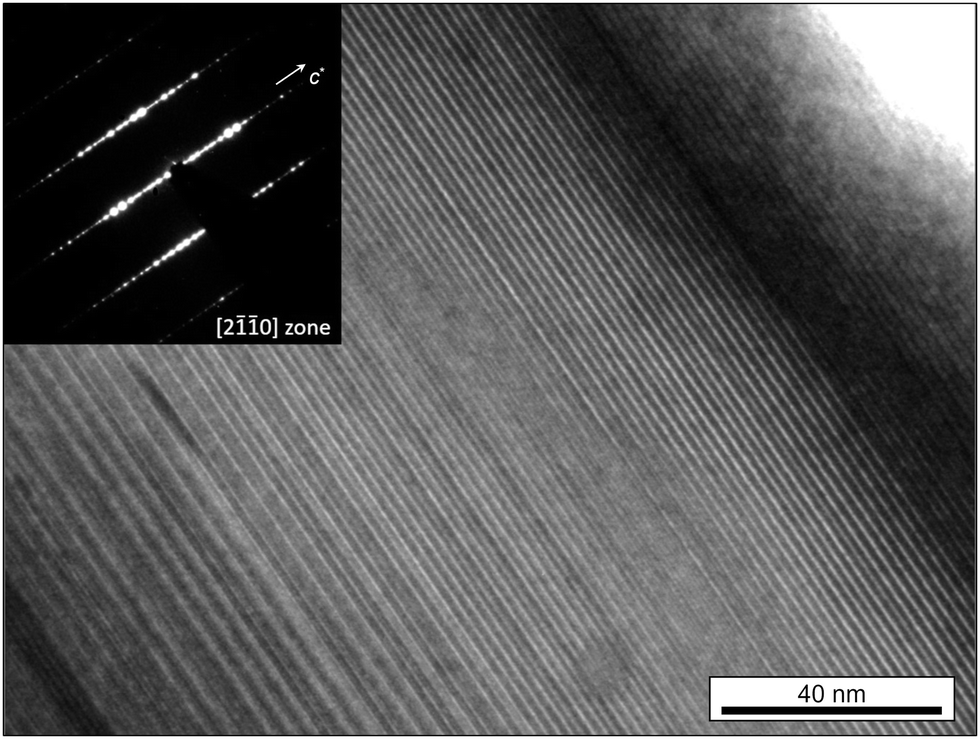 | ||
| Fig. 1 TEM bright-field image showing bright planes expanding laterally straight up to grain boundaries. The corresponding SAED pattern (inset) along the [20] zone axis agrees well with a hexagonal lattice but shows quite complex superstructure reflections along the c*-direction. | ||
Atomic scale STEM-HAADF images taken along the [20] zone axis, reveal an ordering of bright atoms into basal monolayers recurring statistically every 5th to 7th or rarely even 8th layer (Fig. 2A). Interjacent darker layers show a cationic zigzag arrangement identical to the wurtzite structure type. Considering a single basal layer, the atom position of such a small hcp-based layer can only occupy a special position, located at one of the three hex- or threefold axes. These positions can be directly identified from high-resolution STEM-HAADF images. Whereas for layers of the wurtzite structure, only the two tetrahedrally coordinated cation sites are occupied in an alternating zigzag manner like ABAB, all three possible sites are occupied around the bright layers leading to a straight sequence of ccp stacking like ABC. Whenever the quantity of the layer sequence refers to an even number, the sequence along the next adjacent bright layer is reverse to the first one (e.g. CBA), whereas in the case of an odd number, the sequence increases in a cyclic manner (e.g. BCA) and causes a shift in the next layers of the wurtzite structure (e.g. to CACA), since apparently an inversion symmetry in the bright atoms is generally fulfilled. These variations in stacking sequences lead theoretically to a much higher alternation of structural units than the obvious and above reported 5- to maximal 8-fold layers. Any resulting systematic huge stacking, however, is interrupted by a slight statistical variation in the quantity of interjacent layers of the wurtzite structure.
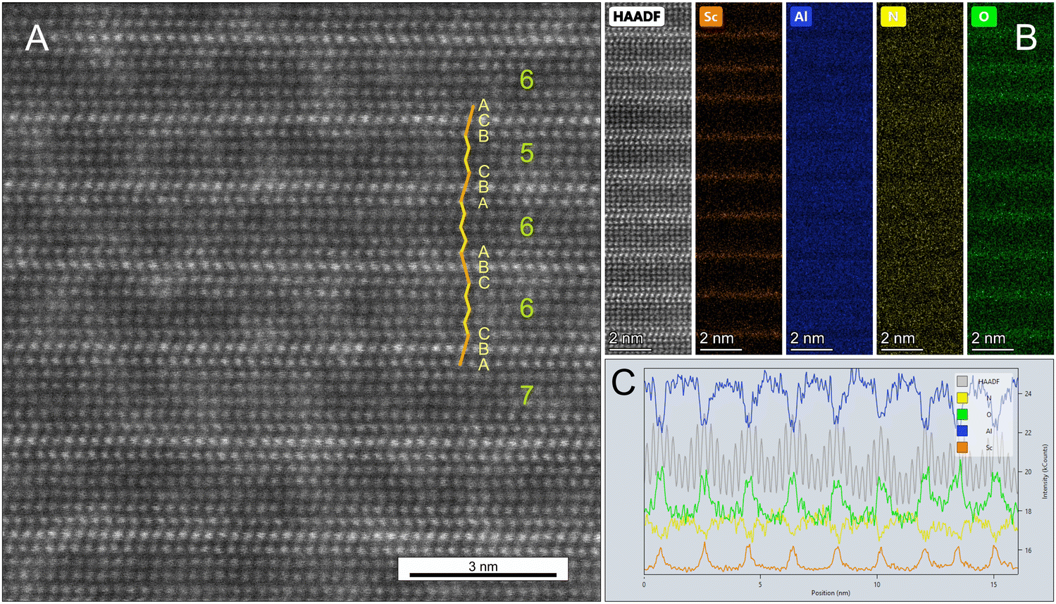 | ||
| Fig. 2 Structural and chemical characterisation of the layered phase after annealing at 1700 °C. (A) STEM-HAADF image at atomic resolution along the [20] zone axis showing the ordering of bright atoms into basal planes. Sequences with hcp-stacking (wurtzite type) are marked in yellow and ccp-stacking in orange, for which detailed stacking positions are provided with A, B and C. The whole number of layers in the sequence is given in green. (B) STEM-EDS elemental maps and (C) line profiles along the c-direction by integrating over 12 unit cells demonstrate the ordering of Sc into monolayers and the affinity of O around these layers. | ||
The elemental distributions are illustrated by atomic scale STEM-EDS maps (Fig. 2B). Sc orders thus entirely into bright monolayers of STEM-HAADF images, replacing a significant portion of Al of that layer, whereas no Sc is detected in the darker AlN layers of the wurtzite structure. The complete ordering of Sc is even more obvious from a line profile of integrated EDS counts over 12 unit cells perpendicular to the c-direction while plotted along the c-direction (Fig. 2C). As a noteworthy second feature, EDS measurements revealed a substantial O content, replacing N at the anionic site. It shows a certain affinity to Sc and is largely spread over the next two neighbouring anionic layers.
Average quantitative EDS analyses (Table 1) of the 1700 °C layered phase result in a Sc-content of almost 5% per formula unit (pfu), which is close to the initial value. Nearly half of the anionic positions are replaced by O leading to speculation that cationic vacancies may likely exist for charge balancing reasons.
| Sample | Al | Velox error | Sc | Velox error | O | Velox error | N | Velox error | x in (Al1−xScx) |
|---|---|---|---|---|---|---|---|---|---|
| Reference [at%] | 47.19 | 4.93 | 2.36 | 0.38 | 2.69 | 0.58 | 47.76 | 4.46 | 0.048 |
| pfu | 0.935 | 0.047 | 0.053 | 0.947 | |||||
| 1400 °C [at%] | 23.53 | 4.33 | 17.91 | 2.81 | 51.38 | 5.67 | 7.18 | 0.83 | 0.432 |
| pfu | 0.402 | 0.306 | 0.877 | 0.123 | |||||
| 1700 °C [at%] | 43.39 | 5.40 | 2.10 | 0.35 | 27.04 | 4.58 | 27.48 | 2.83 | 0.046 |
| pfu | 0.796 | 0.039 | 0.496 | 0.504 |
Further information about the local environment of cations is obtained from EELS spectroscopy by investigating the near-edge fine-structure of the Sc L2,3 edge and Al K edge (Fig. 3). Although theoretically supported interpretations of the Sc L2,3 edge are scarce in the literature, all spectral fine-structures of Sc3+ are assumed to be similar to those of isoelectronic Ti4+, only shifted in energy due to different core potentials.46 Unfortunately, the Sc L lines overlap to a large extent with the N Kα edge at ∼400 eV, but white lines of Sc can be readily distinguished by their stronger intensity and sharper line widths. Both white lines of the Sc L3,2 edge are clearly split by nearly 2 eV for spectra taken from the bright layers (Fig. 3A), which is a feature indicative of octahedral coordination due to crystal field splitting.47,48 Tetrahedral coordination instead, would result in a significantly lower splitting, which would hardly be resolved by EELS. No Sc lines were detectable for interjacent layers and hence show only the underlying N Kα edge.
 | ||
| Fig. 3 EELS spectra of (A) Sc L2,3 and (B) Al K edge. Both spectral lines of Sc L2,3 edge (A) are split by nearly 2 eV indicating octahedral coordination for Sc. Sc L2,3 spectra were superimposed by the broad N K edge, given separately for the 1700 °C spectra at the bottom (dashed). Independent of the annealing temperature, Al K edge spectra (B) of the layered phases are identical to those of AlN of the wurtzite structure (dashed), indicating tetrahedral coordination. | ||
Concerning Al, the near-edge fine-structure of the Al K edge is extensively explored by ab initio calculations.49–51 For oxides, a clear chemical shift of about 2 eV distinguishes spectra from the tetrahedral environment (first line below ∼1567.5 eV) from those of the octahedral environment (first line above ∼1567.5 eV).52 However, the detailed line position is also sensitive to further parameters, e.g., strained bond length.50 For our layered structure, relative line intensities and energetic spacings within the Al K edge features agree well with reference spectra of tetrahedrally coordinated AlN51,53,54 and the total energy of the first line is close to 1570 eV (Fig. 3B). Since all these spectra are identical to those taken from the untreated reference sample of the wurtzite structure as shown below (cf.Fig. 3B), it is assumed that the spectra indicate tetrahedral Al. The energetic position cannot be easily interpreted without detailed modelling of complex effects caused e.g., by slightly deviant bond length due to strain, partial substitution of N by O or correlated vacancies.
TEM characterisation of untreated samples and samples annealed at 1400 °C
Cross-sections of a sample annealed at 1400 °C and the untreated reference show both the characteristic texture of columnar growths of the sputter layer. Individual crystallites are about 50 nm in diameter with pyramidal facets on the top and are slightly twisted and tilted against each other along their columnar axis as well as perpendicular to it (Fig. 4A and B). Hence, these observations explain well the extremely broad and irregular shaped X-ray diffraction profiles as well as AFM roughness data. | ||
| Fig. 4 Cross-sectional STEM bright-field images of the (A) untreated reference sample and (B) sample annealed at 1400 °C. (C) TEM bright-field image of a basal plane section of the sample annealed at 1400 °C indicates the beginning of microstructural equilibration by forming dislocation arrays at small angle grain boundaries. The varying diffraction contrast across the crystallites indicates that crystallites are still strained. At grain boundaries the formation of Sc2O3 nanocrystals and voids are visible but are more obvious in (D) cross-sectional STEM-HAADF images along the [20] zone axis at higher magnification. | ||
The untreated sputter layer is distinguished by a homogeneous distribution of all elements, the absence of any second phase and a smooth interface to the sapphire substrate. In contrast, the sample annealed at 1400 °C shows the first evidence of equilibration processes, e.g. dislocation arrays forming at small angle grain boundaries. Many crystallites still show an internal variation in diffraction contrast and an even larger variation in the contrast between different crystallites (Fig. 4C) indicating that the microstructural equilibration just started, but neither the internal strain from crystallite bending, nor the slight tilting among each other is completely relaxed after that time of annealing. Furthermore, fast exsolution of a second phase along crystallite boundaries is apparent, occasionally coupled with the formation of oval voids (Fig. 4C and D). Such nanocrystals are about 4 to 16 nm in size. According to chemical and crystallographic observations, this second phase is Sc2O3 of the bixbyite structure type (space group Ia![[3 with combining macron]](https://www.rsc.org/images/entities/char_0033_0304.gif) ) showing rather low Al- and N-contents. HAADF patterns show an orientation relationship to the surrounding wurtzite structure of (111)bi‖(0001)w and [11
) showing rather low Al- and N-contents. HAADF patterns show an orientation relationship to the surrounding wurtzite structure of (111)bi‖(0001)w and [11![[2 with combining macron]](https://www.rsc.org/images/entities/char_0032_0304.gif) ]bi‖[100]w as known from other comparable systems.55 But occasionally an additional relationship is observed between {111}bi′‖(101)w and 〈11〉 bi′‖[10]w rarely leading to a twin-like intergrowth of Sc2O3 crystallites along the (113)bi plane as a common intergrowth plane (Fig. 5).
]bi‖[100]w as known from other comparable systems.55 But occasionally an additional relationship is observed between {111}bi′‖(101)w and 〈11〉 bi′‖[10]w rarely leading to a twin-like intergrowth of Sc2O3 crystallites along the (113)bi plane as a common intergrowth plane (Fig. 5).
 | ||
| Fig. 5 STEM-HAADF image of a Sc2O3 nanocrystal at the (Al,Sc)N grain boundary showing a twin-like intergrowth along the common (113)bi plane. The crystal orientation refers to the [20]w zone axis of (Al,Sc)N and [10]bi of Sc2O3. | ||
Besides all that, the sample annealed at 1400 °C also reveals essential evidence of the formation of the novel layered structure, since two diverse stages of Sc-ordering into octahedrally coordinated monolayers are discernible. Most prominent in this context is the scarce and sporadic occurrence of homogeneous nucleation of a tiny Sc-bilayered structure all over the matrix of the wurtzite structure. These Sc-bilayer nuclei generally consist of two octahedral Sc monolayers including one tetrahedral AlN layer in between with a projected lateral spread over 20 to 30 unit cells (Fig. 6A).
 | ||
| Fig. 6 (A) STEM-HAADF image of a Sc-bilayer nucleus formed at 1400 °C by homogeneous nucleation inside an (Al,Sc)N matrix of the wurtzite structure. (B) STEM-HAADF image of a layered phase with only 1 or 2 AlN layers in between Sc-rich layers, formed at 1400 °C by heterogeneous nucleation at the interface between (Al,Sc)N of the wurtzite structure (top panel) and sapphire (bottom panel). | ||
More obvious, however, is a heterogeneous nucleation of a layered structure at the sapphire interface (Fig. 6B) forming a straight and continuous sequence of 10–16 Sc-rich octahedral layers alternating only with one or two Al-bearing wurtzite layers in between. The overall chemical composition is hence much more pronounced in Sc but also in O (cf.Table 1). The growth is likely restrained by a diffusion related depletion of these elements in surrounding regions.
The coordination of Sc is again examined by EELS spectroscopy. Whenever Sc is enriched like in the layered structure close to the sapphire substrate, in the Sc2O3 phase, or even in the bilayer nuclei, we could observe a splitting of the Sc L3,2 lines indicating octahedral coordination (cf.Fig. 3A). In contrast, the Sc-concentration in the matrix of the wurtzite structure is unfortunately too low to gain sufficient spectral statistics. Due to the complete overlap of the Sc L3,2 edge with the N K edge, the contribution of the few percent of Sc vanishes in the noise of the N K edge. EELS spectra of the Al K edge are comparable to those obtained from the sample annealed at 1700 °C (cf.Fig. 3B).
Discussion
Discussion on crystallographic properties and order–disorder relations
The above-described ordering of nominal octahedrally coordinated transition metal cations into self-organised basal monolayers of group III nitrides is unique and intriguing from structural and ordering aspects; but to the best of our knowledge, nothing comparable has been reported before. This appears astonishing, because simply considering cationic size effects, the calculated misfit between a (111) layer of ScN35 to the basal plane of AlN23 accounts for only about 2.4% and is marginal for many other 3d transition metals. Obviously, the strong miscibility gap present in all those chemical systems efficiently prohibits such an intergrowth.The only layered phase reported for the Al1−xScxN system so far is the so-called hexagonal phase, in which a certain widening of the distance between basal anions allows a flipping of the tetrahedral coordinated cations into the basal anion plane and hence forms a fivefold trigonal dipyramidal coordination.39,41 The resulting c/a lattice ratio decreases from 1.6 (wurtzite structure) down to 1.2 and cation positions deviate in the c-direction. This is clearly not observed for our layered structure since d-spacings obtained from (0002) and (102) X-ray profile analyses result in a lattice ratio of 1.596 and no corresponding shift of cations is visible around the Sc-bearing layers in STEM-HAADF images.
The most closely related structure reported so far concerns tiny exsolution nuclei of GdN platelets from Gd-doped GaN. A detailed HRTEM study together with simulations of displacement field maps and energetic minimization of nuclei platelet shape versus misfit strain by DFT modelling revealed that these GdN nuclei form a slightly distorted rock salt bilayer structure with a lateral width of about eight Gd atoms.56 Their further lateral extension is restricted by strain and a low Gd concentration. These nuclei appear somewhat similar to our nuclei observed after annealing at 1400 °C, although ours generate significantly lower strain and are hence less restricted in size. In addition, our octahedrally coordinated Sc-monolayers are generally separated by at least one interjacent tetrahedral AlN layer.
The virtually unlimited lateral extension of our octahedrally coordinated monolayers interjacent to several layers of the wurtzite structure is hence a unique structure type and makes it worth having a closer look into its structural properties. Whereas the crystallographic positions of cations can be directly deduced from STEM-HAADF images as described in the Results section, positions of anions are even not visible in our BF-STEM images. However, anions of a close packed arrangement can also occupy only one of these three special crystallographic sites as well, located at the hex- or threefold axes. Further constraints derive from the local coordination of cations, e.g., for an octahedral coordination, the cation and its upper and lower anions should occupy three different sites, whereas for a tetrahedral coordination in the wurtzite structure, one cationic and anionic basal position is equal but shifted by the crystallographic parameter u along the z-direction. By applying these general constraints it is possible to deduce anionic positions.
The most impressive consequence is that the crystallographic position of each consecutive cationic or anionic layer along the c-direction is strictly determined by the crystallographic position of the previous layers. Only the recurrence of the next Sc-bearing layer occurs somewhat randomly.
Furthermore, it's remarkable to note that first, a cation favouring an octahedral environment will not simply flip out of its tetrahedral position into the next neighbouring octahedral site of that layer. Such a simple behaviour would cause an improbably close distance of face sharing coordination polyhedra towards the next neighbouring tetrahedrally coordinated cation of the next layer. For generating an octahedral layer, the cation will exactly occupy the cationic position expected from the sequence of cation positions in the wurtzite structure type, whereas the octahedral environment originates from a change in the next upper anionic position from the hcp to ccp sequence, the inversion symmetry of which will also affect the subsequent positions of the wurtzite structure. Therefore, the sequence apparently depends more strongly on elastic forces between cationic layers than on known minor energetic differences between anionic hcp or ccp stacking.
Second, the observed reversal of cation stacking in relation to the number of interjacent wurtzite layers is only a consequence of the three-dimensional projection and the octahedral inversion symmetry. Third, the inversion centre in any octahedral layer inevitably causes a polarity inversion in the adjacent layers of the wurtzite structure. Considering a certain octahedral layer, both adjacent layers of tetrahedral coordination are bonded therefore either by their tips resulting in corner-sharing coordination polyhedra, or their basal planes resulting in edge-sharing coordination polyhedra. Polarity inversions in AlN are known from former studies e.g., by applying O during the growth of MOVPE epitaxial AlN films and ferroelectric switching in AlScN.57,58 Whereas Stolyarchuk et al. interpreted the inversion domain boundaries by two interpenetrating wurtzite lattices of a common anion sub-lattice in the aluminium-oxynitride domain boundary,57 the later study claims an assumed polarity inversion via the hexagonal phase.42 Hence both studies differ from our case assuming an alternation in the anionic stacking around octahedral layers.
The above-described sequence of layers indicates that the novel layered Al1−xScxN structure is almost entirely ordered despite the fact that diffraction pattern would suggest a diverse disorder at first glance. Since order parameters are closely related to thermodynamic transitions, it is worth considering order–disorder effects for subsequent thermodynamic considerations on phase formation. First, we observe a complete ordering of Sc-cations into octahedrally coordinated positions, second, cationic positions in wurtzite layers are exclusively occupied by Al. Third, in a more general sense, the stacking of individual layers is well determined and no disorder deviating from the correct stacking of an A, B or C layer is observed, except in the alternation of octahedrally coordinated Sc-rich layers, which varies somewhat randomly around an average value defined by stoichiometry and possibly annealing temperature. In contrast, complete disorder is generally assumed for site occupancies within a certain layer, since no related effects, like superstructure reflections, arising from basal plane ordering are detected. This concerns the disorder of Sc and remaining Al in octahedral layers as well as O and N within the closed packed anionic positions. Due to chemical reasons, O shows a clear affinity towards Sc and cumulates largely within the next two neighbouring anionic layers. This affinity is related to the significantly lower electronegativity of Sc compared to Al. For reasons of charge balancing, related vacancies at the cationic sites are assumed, but we do not observe any indication about ordering.
Discussion on thermodynamic stabilities and phase formation
Finally, the question of whether the novel layered structure will represent either a so far undiscovered, but thermodynamically stable phase in a rarely explored high temperature range, or a further metastable formation inside the miscibility gap, will have a substantial influence on growth conditions to obtain a certain bulk crystal within the Al1−xScxN system. From a structural point of view, the layered structure appears as a homogeneous phase growing by spontaneous nucleation from a metastable phase after activating sufficient diffusion via temperature. This may indicate superior thermodynamic stability. However, PVT growth results and previous thermodynamic simulation11 confirms an extended immiscibility up to much higher temperatures.Hence, its real thermodynamic state of representing another metastable formation is getting more obvious by looking in detail at its first formation during annealing at 1400 °C. Prior to annealing, Sc occupies randomly an electronically less favourable tetrahedral site inside the wurtzite structure, which is clearly a metastable consequence of sputtering.11 The first true homogeneous nucleation of the layered phase is observed by the layered nuclei at 1400 °C occurring simultaneously with the kinetically faster growth of Sc2O3 nanocrystals. However, the growth of Sc2O3 only indicates sufficient strong O-diffusion but it does not represent an energetically favoured Sc-host, because with time and raising temperature it either disappears again by supporting the growth of the layered structure or even more likely, its formation is replaced by faster direct growth of large crystals of the layered phase.
Considering the Gd-bearing system and its exsolution of tiny GdN platelets from Gd-doped GaN,56 DFT modelling revealed that layered nuclei of octahedral coordination could be indeed stable within a nitride host of the wurtzite structure, but their shape and size is restrained by misfit strain. Since for our system, the basal lattice misfit of 2.4% is appreciably lower, it might be compensated elastically inside the octahedral monolayer and hence its formation may expand laterally without restriction. A potential perpendicular misfit during growth is minimal for a monolayer and anyway occurs along the elastically softest direction.42 In comparison to any separate phase formation like Sc2O3 or ScN, there is no requirement for strongly strained or interrupted chemical bonds at its interface, whereas the favourable octahedral coordination is accomplished. An octahedral monolayer thus allows equilibration of cation coordination along short ranges by simultaneous minimisation of surface strain. Hence it can expand above a certain temperature enabling cationic as well as anionic diffusion. In contrast, a separate phase formation e.g., cubic ScN, would need sufficiently more energy and is hence expected at significantly higher temperatures, like for PVT growth conditions, only.
From a thermodynamic point of view, however, the formation of Sc-bearing octahedral monolayers as discussed above, is identical to the formation of exsolution lamellae inside a miscibility gap. The nano-structuring of self-organised octahedral monolayers can thus be considered as a metastable formation of exsolution lamellae of minimal atomic width. The apparent alternation in the number of interjacent layers of the wurtzite structure might therefore only pretend being a disordered structural feature, but in reality it originates from the less-constrained distance to the next exsolution lamellae. Hence, the distance is not determined by crystal symmetry and therefore not a true kind of disorder.
Discussion on the potential role of oxygen
Finally, the high amount of O in the layered structure is another issue presumably affecting its formation. Since these values are significantly higher for the layered structure than previously for the sputtered film, the question arises to which extent O may influence its formation. Considering the proven inhibition of oxidation during our annealing process, all the O should have penetrated from the sapphire substrate into the sputtered film during annealing. The bulk diffusion coefficient of O in an extremely covalent material like AlN is assumed to be very low and is known to depend on several conditions like the impurity level, even of the O concentration itself. Available data range between 5 × 10⁻¹⁵ and 1 × 10⁻¹³ cm2 s−1 at 1700 °C, which would result in a diffusion path length of a few hundred nanometers after 3 h.59,60 However, the columnar microstructure of the sputter layer suggests a significant contribution via grain boundary and pipe diffusion, for which the diffusion coefficient is up to 4 orders of magnitude higher59 and hence enable the postulated diffusion along a few μm.Once present in the system, O is soaked up either by the prior formation of Sc2O3 nanocrystals or even by a probably faster direct formation of the layered phase at 1700 °C. This will likely degrade somewhat all electronic properties concerning conductivity. However, since even scandium oxide itself is still a semiconductor with an ultrawide band gap of ∼5.8 eV,61 it is not assumed that a certain but unknown amount of O will break off the semiconducting properties of (Al,Sc)N, immediately.
Considering its formation from a chemical point of view, O would clearly facilitate the octahedral coordination of Sc, simply because the theoretically more ionic Sc–O bonds in octahedral coordination are chemically favoured for the more electronegative O-ion compared to the more covalent Sc–N bonds in tetrahedral coordination. As a second point, the diffusion of anions appears to be an essential mechanism for the formation of ccp stacking around Sc layers in the layered phase. Whereas N self-diffusion is extremely slow for the wurtzite structure, O–N interdiffusion enhances diffusion whenever significant amounts of O atoms are present60 because related cation vacancies assumed for charge balance reasons would enhance cationic and anionic diffusion within the layered phase. A third important issue is indicated by the observation, that the highest amount of O (cf.Table 1) is coupled to the highest Sc-content and hence the lowest number of AlN layers in between, as occurring in the layered phase formed at the sapphire interphase at the lowest formation temperature of 1400 °C (cf.Fig. 6B). This implies that a series of layered phases with variable sequences of octahedral layers may exist and their occurrence depends on the bulk Sc-content and potentially its formation temperature for kinetic reasons.
Certainly, all these arguments are somewhat valid in general but predominantly affect the kinetics of phase formation. In contrast, the above-described formation mechanism of the layered phase points thermodynamically to the formation of an exsolution lamellae inside a wide miscibility gap, driven by bringing Sc closer to a partial equilibrium state of octahedral coordination without provoking dangling bonds. Therefore, O may shift the formation of the layered phase to somewhat lower temperatures by enhancing kinetics, but it cannot be unambiguously concluded whether O represents an essential component for its formation or a general dependence between oxygen content, layer sequence and formation temperature may exist. Hence, the question on the effect of O cannot be answered solely by our available observations.
Conclusions and practical implications
Annealing experiments on sputtered Sc-bearing AlN of the wurtzite structure revealed a self-organised nano-structuring of Sc into octahedrally coordinated monolayers, which is intriguing from structural or atomic ordering aspects. The above discussion has shown that the metastable formation of the layered structure resembles exsolution lamellae of atomic minimal width from a thermodynamic point of view. Its spontaneous formation is related to local equilibration processes, driven largely by a change in the coordination of Sc. It requires diffusion of cations and anions, which might at least be enhanced by available O-content.Therefore, the equilibration process shows for the first time that the metastable existence of the Sc-bearing phase of the wurtzite structure is limited in temperature. This entails substantial implications for the (Al,Sc)N material of wurtzite structure grown for electronic devices. Any post-annealing or even suitable high and prolonged MOCVD conditions may somehow increase the crystallinity by diffusion but may also degrade the tetrahedral environment of Sc. This eventually provides another explanation why the piezoelectric coefficient may decrease after excessive annealing as reported in previous studies.36 In order to obtain excellent materials for electronic devices, the major consequence would be to apply metastable growth techniques that are capable of growing well-crystallized materials of wurtzite structure in a temperature range as high as possible to achieve a good quality instantaneously, but below the onset of significant diffusion to prevent structural degradation. Such a suitable temperature for growth might presumably range between 1000° and 1200 °C. Recent advances have shown that this could be successfully achieved by MBE growth29,30,62 or MOCVD.32,33 However, subsequent inter-diffusion or oxidation during electronic device operation could also trigger migration processes at significantly lower temperatures. Therefore, the thermal stability of AlScN devices operating at relatively high temperatures should be carefully tested.
Author contributions
Ulrich Bläβ: conceptualization (lead); validation (lead); investigation (equal); data curation (equal); formal analysis (equal); visualization (lead); writing – original draft (lead); writing – review & editing (lead); supervision (equal); and project administration (equal). Mingjian Wu: investigation (equal); data curation (equal); and formal analysis (equal). Boris Epelbaum: investigation (equal) and formal analysis (supporting). Elke Meissner: conceptualization (equal); supervision (lead); project administration (equal); and funding acquisition (lead).Data availability
All data supporting the findings of this article are presented within figures and tables of the article.Conflicts of interest
There are no conflicts to declare.Acknowledgements
Part of the work was supported by the Fraunhofer internally founded project Leistungselektronik2020+. The authors gratefully acknowledge Prof. O. Ambacher (Fraunhofer IAF, Freiburg) for providing sputtered (Al,Sc)N samples from Evatec, Switzerland. In addition, the authors would like to thank Sepideh Faraji for measuring XRD line profiles and Dr Sven Besendörfer for measuring surface roughness values by AFM.References
- O. Ambacher, J. Phys. D: Appl. Phys., 1998, 31, 2653–2710 CrossRef CAS.
- H. Amano, Y. Baines, E. Beam, M. Borga, T. Bouchet, P. R. Chalker, M. Charles, K. J. Chen, N. Chowdhury, R. Chu, C. de Santi, M. M. de Souza, S. Decoutere, L. Di Cioccio, B. Eckardt, T. Egawa, P. Fay, J. J. Freedsman, L. Guido, O. Häberlen, G. Haynes, T. Heckel, D. Hemakumara, P. Houston, J. Hu, M. Hua, Q. Huang, A. Huang, S. Jiang, H. Kawai, D. Kinzer, M. Kuball, A. Kumar, K. B. Lee, X. Li, D. Marcon, M. März, R. McCarthy, G. Meneghesso, M. Meneghini, E. Morvan, A. Nakajima, E. M. S. Narayanan, S. Oliver, T. Palacios, D. Piedra, M. Plissonnier, R. Reddy, M. Sun, I. Thayne, A. Torres, N. Trivellin, V. Unni, M. J. Uren, M. van Hove, D. J. Wallis, J. Wang, J. Xie, S. Yagi, S. Yang, C. Youtsey, R. Yu, E. Zanoni, S. Zeltner and Y. Zhang, J. Phys. D: Appl. Phys., 2018, 51, 163001 CrossRef.
- J. Y. Tsao, S. Chowdhury, M. A. Hollis, D. Jena, N. M. Johnson, K. A. Jones, R. J. Kaplar, S. Rajan, C. G. van de Walle, E. Bellotti, C. L. Chua, R. Collazo, M. E. Coltrin, J. A. Cooper, K. R. Evans, S. Graham, T. A. Grotjohn, E. R. Heller, M. Higashiwaki, M. S. Islam, P. W. Juodawlkis, M. A. Khan, A. D. Koehler, J. H. Leach, U. K. Mishra, R. J. Nemanich, R. C. N. Pilawa-Podgurski, J. B. Shealy, Z. Sitar, M. J. Tadjer, A. F. Witulski, M. Wraback and J. A. Simmons, Adv. Electron. Mater., 2018, 4, 1600501 CrossRef.
- A. L. Hickman, R. Chaudhuri, S. J. Bader, K. Nomoto, L. Li, J. C. M. Hwang, H. Grace Xing and D. Jena, Semicond. Sci. Technol., 2021, 36, 44001 CrossRef CAS.
- W. A. Doolittle, C. M. Matthews, H. Ahmad, K. Motoki, S. Lee, A. Ghosh, E. N. Marshall, A. L. Tang, P. Manocha and P. D. Yoder, Appl. Phys. Lett., 2023, 123, 070501 CrossRef CAS.
- L. F. Eastman and U. K. Mishra, IEEE Spectrum, 2002, 39, 28–33 Search PubMed.
- K. A. Jones, T. P. Chow, M. Wraback, M. Shatalov, Z. Sitar, F. Shahedipour, K. Udwary and G. S. Tompa, J. Mater. Sci., 2015, 50, 3267–3307 CrossRef CAS.
- S. Besendörfer, E. Meissner, F. Medjdoub, J. Derluyn, J. Friedrich and T. Erlbacher, Sci. Rep., 2020, 10, 17252 CrossRef.
- M. Akiyama, T. Kamohara, K. Kano, A. Teshigahara, Y. Takeuchi and N. Kawahara, Adv. Mater., 2009, 21, 593–596 CrossRef CAS.
- M. Akiyama, K. Kano and A. Teshigahara, Appl. Phys. Lett., 2009, 95, 162107 CrossRef.
- M. A. Moram and S. Zhang, J. Mater. Chem. A, 2014, 2, 6042–6050 RSC.
- M. A. Caro, S. Zhang, M. Ylilammi, T. Riekkinen, M. A. Moram, O. Lopez-Acevedo, J. Molarius and T. Laurila, J. Phys.: Condens. Matter, 2015, 27, 245901 CrossRef.
- D. Jena, R. Page, J. Casamento, P. Dang, J. Singhal, Z. Zhang, J. Wright, G. Khalsa, Y. Cho and H. G. Xing, Jpn. J. Appl. Phys., 2019, 58, SC0801 CrossRef CAS.
- A. Ding, L. Kirste, Y. Lu, R. Driad, N. Kurz, V. Lebedev, T. Christoph, N. M. Feil, R. Lozar, T. Metzger, O. Ambacher and A. Žukauskaitė, Appl. Phys. Lett., 2020, 116, 101903 CrossRef CAS.
- O. Ambacher, B. Christian, N. Feil, D. F. Urban, C. Elsässer, M. Prescher and L. Kirste, J. Appl. Phys., 2021, 130, 045102 CrossRef CAS.
- X. Liu, D. Wang, K.-H. Kim, K. Katti, J. Zheng, P. Musavigharavi, J. Miao, E. A. Stach, R. H. Olsson and D. Jariwala, Nano Lett., 2021, 21, 3753–3761 CrossRef CAS PubMed.
- J. Casamento, T.-S. Nguyen, Y. Cho, C. Savant, T. Vasen, S. Afroz, D. Hannan, H. Xing and D. Jena, Appl. Phys. Lett., 2022, 121, 192101 CrossRef CAS.
- M. Yassine, A. Nair, J. Fammels, E. Wade, Z. Fu, A. Yassine, L. Kirste and O. Ambacher, J. Appl. Phys., 2022, 132, 114101 CrossRef CAS.
- G. Schönweger, N. Wolff, M. R. Islam, M. Gremmel, A. Petraru, L. Kienle, H. Kohlstedt and S. Fichtner, Adv. Sci., 2023, 10, 2302296 CrossRef PubMed.
- P. Wang, D. Wang, S. Mondal, M. Hu, J. Liu and Z. Mi, Semicond. Sci. Technol., 2023, 38, 043002 CrossRef CAS.
- J. Gao, Y.-C. Chien, L. Li, H. K. Lee, S. Samanta, B. Varghese, H. Xiang, M. Li, C. Liu, Y. Zhu, L. Chen and K.-W. Ang, Small, 2024, 20, 2404711 CrossRef CAS.
- G. Giribaldi, L. Colombo, P. Simeoni and M. Rinaldi, Nat. Commun., 2024, 15, 304 CrossRef CAS.
- C. Höglund, J. Birch, B. Alling, J. Bareño, Z. Czigány, P. O. Å. Persson, G. Wingqvist, A. Zukauskaite and L. Hultman, J. Appl. Phys., 2010, 107, 123515 CrossRef.
- G. Wingqvist, F. Tasnádi, A. Zukauskaite, J. Birch, H. Arwin and L. Hultman, Appl. Phys. Lett., 2010, 97, 112902 CrossRef.
- R. Matloub, M. Hadad, A. Mazzalai, N. Chidambaram, G. Moulard, C. S. Sandu, T. Metzger and P. Muralt, Appl. Phys. Lett., 2013, 102, 152903 CrossRef.
- M. Baeumler, Y. Lu, N. Kurz, L. Kirste, M. Prescher, T. Christoph, J. Wagner, A. Žukauskaitė and O. Ambacher, J. Appl. Phys., 2019, 126, 045715 CrossRef.
- S. Ndiaye, C. Elias, A. Diagne, H. Rotella, F. Georgi, M. Hugues, Y. Cordier, F. Vurpillot and L. Rigutti, Appl. Phys. Lett., 2023, 123, 162102 CrossRef CAS.
- I. Streicher, S. Leone, M. Zhang, T. S. Tlemcani, M. Bah, P. Straňák, L. Kirste, M. Prescher, A. Yassine, D. Alquier and O. Ambacher, Adv. Funct. Mater., 2024, 34, 2403027 CrossRef CAS.
- M. T. Hardy, B. P. Downey, N. Nepal, D. F. Storm, D. S. Katzer and D. J. Meyer, Appl. Phys. Lett., 2017, 110, 162104 CrossRef.
- K. Frei, R. Trejo-Hernández, S. Schütt, L. Kirste, M. Prescher, R. Aidam, S. Müller, P. Waltereit, O. Ambacher and M. Fiederle, Jpn. J. Appl. Phys., 2019, 58, SC1045 CrossRef CAS.
- A. J. Green, J. K. Gillespie, R. C. Fitch, D. E. Walker, M. Lindquist, A. Crespo, D. Brooks, E. Beam, A. Xie, V. Kumar, J. Jimenez, C. Lee, Y. Cao, K. D. Chabak and G. H. Jessen, IEEE Electron Device Lett., 2019, 40, 1056–1059 CAS.
- S. Leone, J. Ligl, C. Manz, L. Kirste, T. Fuchs, H. Menner, M. Prescher, J. Wiegert, A. Žukauskaitė, R. Quay and O. Ambacher, Phys. Status Solidi RRL, 2020, 14, 1900535 CrossRef CAS.
- C. Manz, S. Leone, L. Kirste, J. Ligl, K. Frei, T. Fuchs, M. Prescher, P. Waltereit, M. A. Verheijen, A. Graff, M. Simon-Najasek, F. Altmann, M. Fiederle and O. Ambacher, Semicond. Sci. Technol., 2021, 36, 034003 CrossRef CAS.
- J. C. Schuster and J. Bauer, J. Less-Common Met., 1985, 109, 345–350 CrossRef CAS.
- W. Lengauer, J. Solid State Chem., 1988, 76, 412–415 CrossRef CAS.
- P. M. Mayrhofer, P. O. Å. Persson, A. Bittner and U. Schmid, Microsyst. Technol., 2016, 22, 1679–1689 CrossRef CAS.
- S. Zhang, D. Holec, W. Y. Fu, C. J. Humphreys and M. A. Moram, J. Appl. Phys., 2013, 114, 133510 CrossRef.
- A. Dittmar, J. Wollweber, M. Schmidbauer, D. Klimm, C. Hartmann and M. Bickermann, J. Cryst Growth, 2018, 500, 74–79 CrossRef CAS.
- N. Farrer and L. Bellaiche, Phys. Rev. B: Condens. Matter Mater. Phys., 2002, 66, 201203 CrossRef.
- V. Ranjan, S. Bin-Omran, D. Sichuga, R. S. Nichols, L. Bellaiche and A. Alsaad, Phys. Rev. B: Condens. Matter Mater. Phys., 2005, 72, 085315 CrossRef.
- C. Constantin, H. Al-Brithen, M. B. Haider, D. Ingram and A. R. Smith, Phys. Rev. B: Condens. Matter Mater. Phys., 2004, 70, 193309 CrossRef.
- F. Tasnádi, B. Alling, C. Höglund, G. Wingqvist, J. Birch, L. Hultman and I. A. Abrikosov, Phys. Rev. Lett., 2010, 104, 137601 CrossRef PubMed.
- D. Solonenko, C. Lan, C. Schmidt, C. Stoeckel, K. Hiller and D. R. T. Zahn, J. Mater. Sci., 2020, 55, 17061–17071 CrossRef CAS.
- H. Miyake, C.-H. Lin, K. Tokoro and K. Hiramatsu, J. Cryst. Growth, 2016, 456, 155–159 CrossRef CAS.
- E. van Cappellen and J. C. Doukhan, Ultramicroscopy, 1994, 53, 343–349 CrossRef CAS.
- J. Graetz, C. C. Ahn, H. Ouyang, P. Rez and B. Fultz, Phys. Rev. B: Condens. Matter Mater. Phys., 2004, 69, 235103 CrossRef.
- R. D. Leapman, L. A. Grunes and P. L. Fejes, Phys. Rev. B: Condens. Matter Mater. Phys., 1982, 26, 614–635 CrossRef CAS.
- S. Nayak, M. Baral, M. Gupta, J. Singh, M. Garbrecht, T. Ganguli, S. M. Shivaprasad and B. Saha, Phys. Rev. B, 2019, 99, 161117 CrossRef CAS.
- R. Brydson, J. Phys. D: Appl. Phys., 1996, 29, 1699–1708 CrossRef CAS.
- J. A. van Bokhoven, T. Nabi, H. Sambe, D. E. Ramaker and D. C. Koningsberger, J. Phys.: Condens. Matter, 2001, 13, 10247–10260 CrossRef CAS.
- M. Mogi, T. Yamamoto, T. Mizoguchi, K. Tatsumi, S. Yoshioka, S. Kameyama, I. Tanaka and H. Adachi, Mater. Trans., 2004, 45, 2031–2034 CrossRef CAS.
- D. Li, G. M. Bancroft, M. E. Fleet, X. H. Feng and Y. Pan, Am. Mineral., 1995, 80, 432–440 CAS.
- V. Serin, C. Colliex, R. Brydson, S. Matar and F. Boucher, Phys. Rev. B: Condens. Matter Mater. Phys., 1998, 58, 5106–5115 CrossRef CAS.
- T. Mizoguchi, I. Tanaka, M. Kunisu, M. Yoshiya, H. Adachi and W. Y. Ching, Micron, 2003, 34, 249–254 CrossRef CAS PubMed.
- S. Sadofev, Y. Cho, O. Brandt, M. Ramsteiner, R. Calarco, H. Riechert, S. C. Erwin, Z. Galazka, M. Korytov, M. Albrecht, R. Uecker and R. Fornari, Appl. Phys. Lett., 2012, 101, 172102 CrossRef.
- M. Wu, S. C. Erwin and A. Trampert, Acta Mater., 2014, 76, 87–93 CrossRef CAS.
- N. Stolyarchuk, T. Markurt, A. Courville, K. March, J. Zúñiga-Pérez, P. Vennéguès and M. Albrecht, Sci. Rep., 2018, 8, 14111 CrossRef CAS.
- N. Wolff, S. Fichtner, B. Haas, M. R. Islam, F. Niekiel, M. Kessel, O. Ambacher, C. Koch, B. Wagner, F. Lofink and L. Kienle, J. Appl. Phys., 2021, 129, 034103 CrossRef CAS.
- H. Solmon, D. Robinson and R. Dieckmann, J. Am. Ceram. Soc., 1994, 77, 2841–2848 CrossRef CAS.
- M. Sternitzke and G. Müller, J. Am. Ceram. Soc., 1994, 77, 737–742 CrossRef CAS.
- A. Belosludtsev, K. Juškevičius, L. Ceizaris, R. Samuilovas, S. Stanionytė, V. Jasulaitienė and S. Kičas, Appl. Surf. Sci., 2018, 427, 312–318 CrossRef CAS.
- C. Elias, M. Nemoz, H. Rotella, F. Georgi, S. Vézian, M. Hugues and Y. Cordier, APL Mater., 2023, 11, 031105 CrossRef CAS.
| This journal is © The Royal Society of Chemistry 2025 |