
 Open Access Article
 This Open Access Article is licensed under a Creative Commons Attribution-Non Commercial 3.0 Unported Licence
Very high frequency (∼100 MHz) plasma enhanced atomic layer deposition high-κ hafnium zirconium oxide capacitors near morphotropic phase boundary with low current density & high-κ for DRAM technology†
Ketong
Yang
,
Hunbeom
Shin
,
Seungyeob
Kim
,
Taeseung
Jung
and
Sanghun
Jeon
 *
*
School of electrical engineering, Korea Advanced Institute of Science and Technology, 291 Daehak-ro, Yuseong-gu, Daejeon 34141, Korea. E-mail: jeonsh@kaist.ac.kr
First published on 11th February 2025
Abstract
Hafnium dioxide-based ferroelectric (FE) films are emerging as pivotal materials for advanced memory storage and neuromorphic computing, particularly in ultra-scaled dynamic random-access memory (DRAM) technologies. To meet the stringent DRAM performance requirements—dielectric constants (κ) exceeding 60 and leakage current densities below 10−6 A cm−2 at 0.8 V—hafnium zirconium oxide (HZO) films engineered near the morphotropic phase boundary (MPB) are leading candidates. These films offer a favorable balance of high dielectric properties and reduced equivalent oxide thickness while managing leakage. However, film thinning often escalates leakage currents, presenting a significant design challenge. Moreover, interfacial damage induced by conventional deposition techniques can undermine dielectric stability. Here, we present a novel approach utilizing very high frequency (VHF, 100 MHz) plasma-enhanced atomic layer deposition (PE-ALD) to fabricate 4.5 nm HZO films with superior crystalline quality and minimized oxygen vacancies. This method yields an impressive dielectric constant of 64.47, markedly surpassing radio frequency-deposited counterparts. Notably, at elevated temperatures up to 389 K, the dielectric constant reaches 69.9, approaching the theoretical tetragonal-phase limit. Our results demonstrate the transformative potential of VHF PE-ALD in optimizing HZO film properties, establishing a compelling pathway for future high-performance DRAM applications.
1. Introduction
The discovery of ferroelectricity in HfO2 and ZrO2 thin films in 20121 has sparked considerable interest, driving extensive research into hafnia-based ferroelectrics for next-generation DRAM and flash memory applications.2,3 Among these, ferroelectric DRAM employing a 1T1C configuration is particularly promising for future nonvolatile memory due to its high speed and low power consumption.4,5 Unlike conventional DRAM and flash memories that rely on electron charge for data storage, ferroelectric memories utilize the polarization states of ferroelectric materials, making their performance highly dependent on the intrinsic properties of the ferroelectric films.6,7 However, key challenges remain, including the need to achieve a high dielectric constant (κ), minimize leakage currents, and optimize the overall material properties.8,9Recent advancements have shown that hafnium zirconium oxide (HZO) films, engineered near the morphotropic phase boundary (MPB), can exhibit high κ values while maintaining acceptable leakage current densities.8,10 The o/t-phase of HZO near the MPB is characterized by elevated κ values when subjected to voltages surpassing the coercive voltage (VC). For DRAM cell applications, it is critical that the VC of HZO remains below 0.6 V, aligning with the operational voltage of DDR5.11 Furthermore, the compatibility of MPB HZO with CMOS technology, along with the advantages of advanced fabrication methods like atomic layer deposition (ALD), reinforces its potential for cutting-edge memory applications.9,12
ALD is a precision deposition technique that alternates the pulsing of precursor gases onto a substrate, facilitating chemisorption and self-limiting surface reactions. This approach enables the formation of highly conformal thin films over large areas, making it ideal for complex microelectronic structures.13–16 Plasma-enhanced atomic layer deposition (PE-ALD) further advances this capability by enhancing film quality at reduced temperatures. By generating highly reactive species, PE-ALD enables the deposition of films on heat-sensitive materials, improves purity, and accelerates growth rates.17,18 Nevertheless, the use of plasma introduces challenges, including potential plasma-induced damage to underlying layers, which can increase leakage currents and interfacial defects.19–21
Emerging research has focused on very high frequency (VHF) PE-ALD, which operates between 60 and 150 MHz. This technique shows promise in mitigating plasma damage during deposition by lowering ion bombardment energy, thereby reducing defects and improving the dielectric properties of thin films.22,23 VHF plasma enhances the quality of deposited films, enabling them to approach theoretical limits for dielectric constant and leakage current.24,25
In this study, we investigate the impact of VHF (100 MHz) PE-ALD on the crystallization and electrical properties of ultra-thin HZO films near the MPB. The high plasma density combined with reduced ion bombardment energy in VHF PE-ALD significantly minimizes defect densities, especially oxygen vacancies. This defect reduction prevents the formation of non-conductive dead layers and promotes the effective establishment of the MPB phase. Consequently, VHF-deposited HZO capacitors exhibit superior electrical performance, achieving a high κ value of 64.47, a low leakage current density of 1.47 × 10⁻⁶ A cm−2 at 0.8 V, and a trap state energy of 0.58 eV. Furthermore, the κ value increases to 69.1 at 393 K, approaching the theoretical limit for the tetragonal phase. These results underscore the potential of VHF PE-ALD HZO films for future high-performance DRAM and flash memory technologies.
2. Methods
2.1. Fabrication
Two metal–ferroelectric–metal (MFM) capacitor structures (TiN/HZO/TiN) were fabricated using PE-ALD at different power frequencies to investigate the impact of VHF plasma on the electrical properties of HZO films. Initially, 50 nm thick TiN bottom electrodes were deposited onto SiO2 (300 µm)/Si substrates via DC sputtering at room temperature with a power of 150 W. Subsequently, HZO films with thicknesses of 3, 4.5, 5, 6, and 8 nm and Hf![[thin space (1/6-em)]](https://www.rsc.org/images/entities/char_2009.gif) :Zr ratios of 1:1, 1:2, and 1:3 was deposited at 320 °C using PE-ALD, applying varied power frequencies (VHF 100 MHz, RF 13.56 MHz). The specific ALD deposition process is as follows: The process begins with the introduction of a precursor into the chamber. The precursor chemisorbs onto reactive surface sites, introducing Hf or Zr ions (step 1). Any excess precursor is then flushed out with a gas purge (step 2). Subsequently, oxygen is introduced, and plasma is generated by applying a voltage, inducing chemical reactions between the co-reactants and precursor fragments to form a monolayer (step 3). Finally, a secondary gas purge is used to remove the reaction by-products and any residual co-reactants (step 4). A 1 nm thick TiN layer, serving as the top electrode (TE), was deposited onto the HZO films using the same method at 300 °C. The precursors for Hf and Zr were employed accordingly, with TiCl4 used for the Ti source. Oxygen (O2) gas acted as the oxygen source, while ammonia (NH3) was used for nitridation. After forming the electrode, 10 nm of Ti and 50 nm of Pt were sequentially deposited via electron beam evaporation under a shadow mask. The patterned TiN TE was then selectively etched using a NH4OH:H2O2:H2O (1:2:5) solution at 37 °C, with Pt serving as the hard mask, followed by rapid thermal annealing (RTA) at 600 °C for 10 seconds to crystallize the HZO films.
:Zr ratios of 1:1, 1:2, and 1:3 was deposited at 320 °C using PE-ALD, applying varied power frequencies (VHF 100 MHz, RF 13.56 MHz). The specific ALD deposition process is as follows: The process begins with the introduction of a precursor into the chamber. The precursor chemisorbs onto reactive surface sites, introducing Hf or Zr ions (step 1). Any excess precursor is then flushed out with a gas purge (step 2). Subsequently, oxygen is introduced, and plasma is generated by applying a voltage, inducing chemical reactions between the co-reactants and precursor fragments to form a monolayer (step 3). Finally, a secondary gas purge is used to remove the reaction by-products and any residual co-reactants (step 4). A 1 nm thick TiN layer, serving as the top electrode (TE), was deposited onto the HZO films using the same method at 300 °C. The precursors for Hf and Zr were employed accordingly, with TiCl4 used for the Ti source. Oxygen (O2) gas acted as the oxygen source, while ammonia (NH3) was used for nitridation. After forming the electrode, 10 nm of Ti and 50 nm of Pt were sequentially deposited via electron beam evaporation under a shadow mask. The patterned TiN TE was then selectively etched using a NH4OH:H2O2:H2O (1:2:5) solution at 37 °C, with Pt serving as the hard mask, followed by rapid thermal annealing (RTA) at 600 °C for 10 seconds to crystallize the HZO films.
2.2. Electrical analysis
The electrical properties of the capacitors were evaluated using a Keithley 4200 semiconductor parameter analyzer. Key measurements included polarization–voltage (P–V) curves, current density–voltage (J–V) characteristics, endurance, polarization change ratios, and leakage current density.2.3. Material analysis
The crystallographic characteristics and residual stresses of HZO thin films were assessed using grazing incidence X-ray diffraction (GIXRD) conducted on a Rigaku D/MAX-2500 diffractometer. The thickness of deposited HZO films were measured using ellipsometer (SE200BM-M300).3. Results and discussion
Fig. 1a illustrates the extent of damage to HZO films deposited via conventional radio frequency (RF) PE-ALD. The high-energy ion bombardment in RF PE-ALD introduces defects, leading to increased leakage currents and a reduced dielectric constant. In contrast, VHF plasma, characterized by lower ion bombardment energy (Ei), effectively minimizes this plasma-induced damage. Ei decreases as the frequency increases, as shown in ref. 26. In evaluations based on inhomogeneous plasma modes, the Ei for RF plasma was calculated to be 1420 eV, which is approximately three times higher than that of VHF plasma at 438 eV.27Fig. 1b illustrates the phase evolution of HZO films with increasing Zr doping ratios, showing a transition from ferroelectric (FE) to morphotropic phase boundary (MPB) and eventually to antiferroelectric (AFE) phases.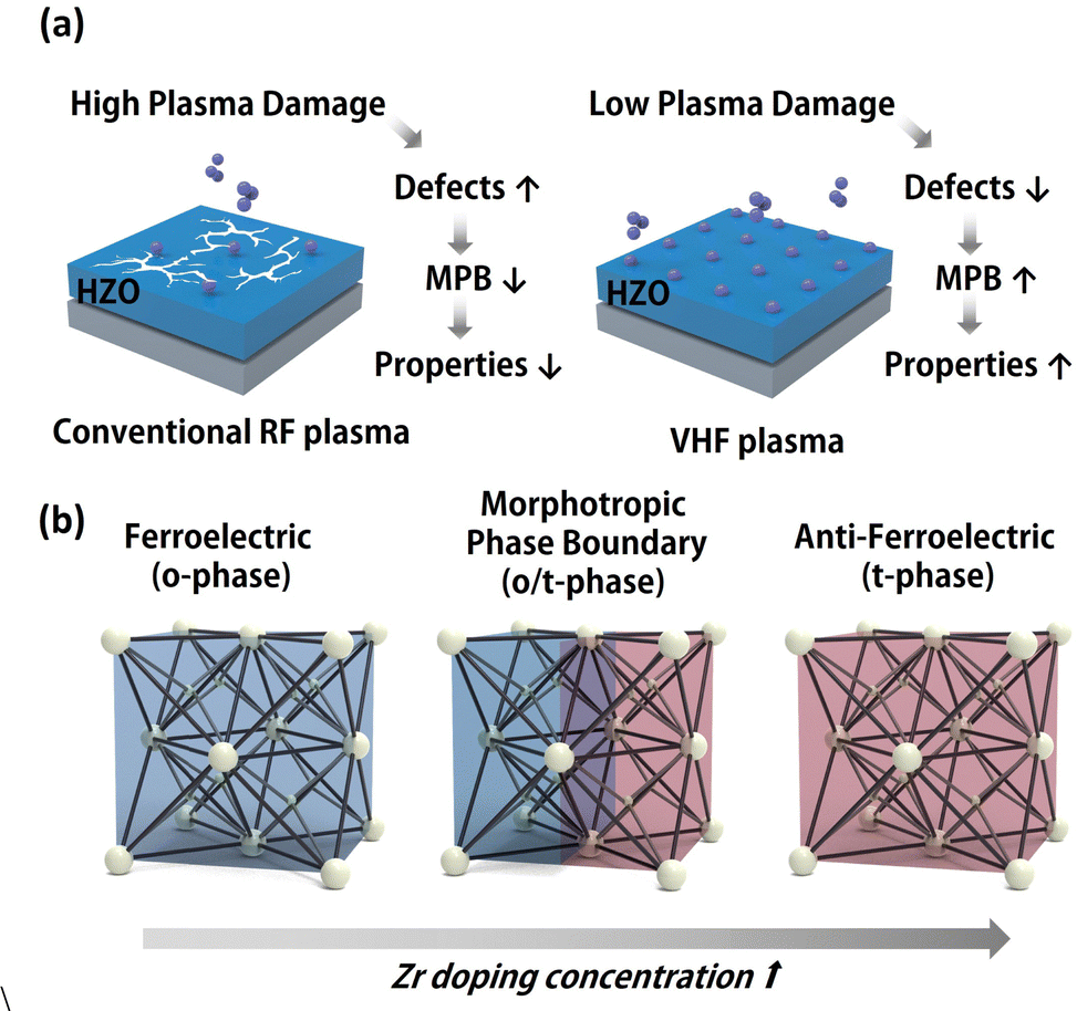 | ||
| Fig. 1 Schematic depiction of VHF plasma and MPB Changing Trends (a) Schematic depiction of plasma damage in conventional RF plasma and VHF plasma. (b) MPB HZO phase tuning processes, by concentration (FE, MPB, AFE). | ||
Fig. 2 presents the polarization–voltage (P–V) and capacitance–voltage (C–V) characteristics of 1:1 HZO samples deposited using VHF and RF PE-ALD, evaluated across various thicknesses. The remanent polarization (Pr) of the VHF-deposited HZO reaches 25.1 µC cm−2, marking a 16.2% improvement compared to the RF-deposited HZO, which shows a Pr value of 21.6 µC cm−2. As film thickness increases, the Pr value of VHF-deposited HZO rises from 12.1 µC cm−2 at 4.5 nm to 25.1 µC cm−2 at 8 nm, while the Pr of RF-deposited HZO increases from 12.6 µC cm−2 at 4.5 nm to 21.3 µC cm−2 at 8 nm. Notably, VHF-deposited HZO at 4.5 nm exhibits prominent morphotropic phase boundary (MPB) characteristics and a high dielectric constant (κ) of 64.47, which is 9.1% higher than the 59.08 observed for RF-deposited HZO. Additionally, the coercive voltage of VHF-deposited HZO at 4.5 nm is 0.5 V, well below the 0.6 V threshold required for DDR5 applications.
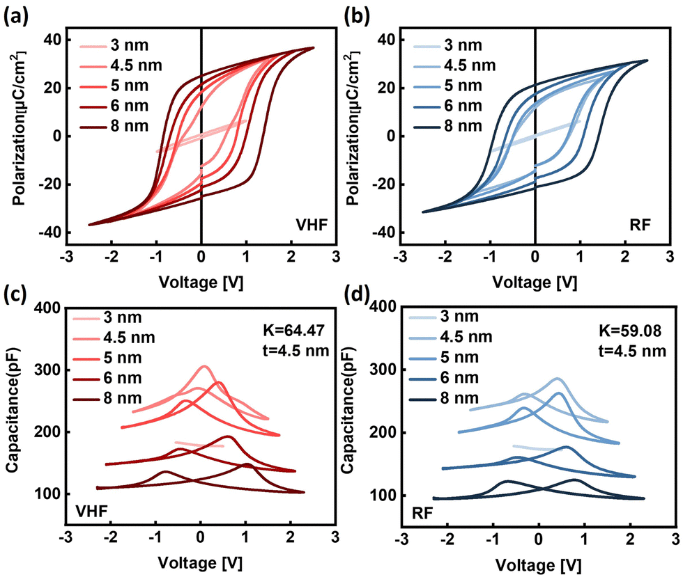 | ||
| Fig. 2 (a) Variation of Polarization–Voltage (P–V) of VHF-deposited HZO (Hf:Zr = 1:1) film with thickness. (b) Variation of P–V of RF-deposited HZO (Hf:Zr = 1:1) film with thickness. (c) Variation of capacitance–voltage (C–V) of VHF-deposited HZO (Hf:Zr = 1:1) film with thickness. (d) Variation of C–V of RF-deposited HZO (Hf:Zr = 1:1) film with thickness. | ||
A detailed analysis of the high-κ value in VHF-deposited HZO reveals its superior performance compared to RF-deposited HZO, particularly for film thicknesses below 6 nm. This enhanced κ-value in VHF-deposited HZO is primarily attributed to reduced plasma-induced damage during VHF deposition (Fig. 3a). As film thickness decreases, the impact of the defects on the film's electrical performance becomes more pronounced. A well-known issue with HZO ferroelectric films is the “wake-up effect”, which is generally associated with intrinsic defects and damage incurred during deposition. This effect serves as an indicator of film quality, as it reflects changes in the κ-value under cycling, correlating with defect density and structural integrity.28,29Fig. 3b illustrates the trend in κ-value variation under a unipolar pulse at 0.8 V, simulating typical DRAM operating conditions. The κ-value change rate for VHF-deposited HZO is nearly half that of RF-deposited HZO, with VHF-deposited HZO exhibiting a 2.5% change at 1011 cycles, compared to 7.8% for RF-deposited HZO. Additionally, Fig. 3c displays the capacitance behavior of 4.5 nm VHF-deposited HZO across a temperature range of 298 K to 423 K. The capacitance increases with temperature, peaking at 393 K, where the dielectric constant reaches 69.1, approaching the theoretical maximum of 70 (Fig. 3d). This temperature-dependent performance underscores the stability and high dielectric potential of VHF-deposited HZO films, demonstrating their suitability for high-κ applications.
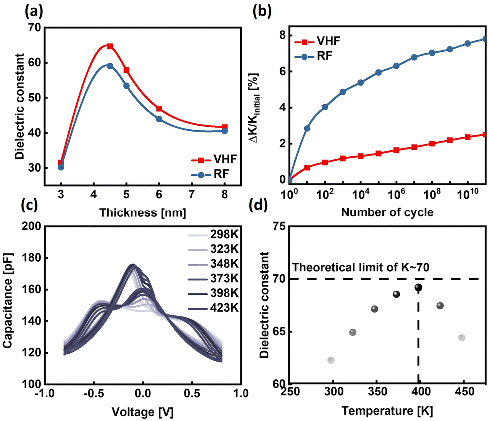 | ||
| Fig. 3 (a) Comparison of dielectric constants for the VHF and RF-deposited PE-ALD processed HZO (Hf:Zr = 1:1) films at various thicknesses in room temperature. (b) Comparison of dielectric constants change rate for the VHF and RF-deposited PE-ALD processed HZO (Hf:Zr = 1:1) films with number of cycles. (c) Temperature effect on C–V curves of 4.5 nm HZO (Hf:Zr = 1:1) film. (d) Temperature effect on high κ values of 4.5 nm HZO (Hf:Zr = 1:1) film. | ||
Another significant advantage of VHF-deposited HZO is its remarkably lower leakage current. As depicted in Fig. 4a, the leakage current of VHF-deposited HZO remains consistently lower than that of RF-deposited HZO across different film thicknesses at an applied voltage of 0.8 V. Specifically, at a thickness of 4.5 nm, VHF-deposited HZO achieves a leakage current density of 1.47 × 10⁻⁶ A cm−2, which is 10 times lower than the 4.1 × 10⁻⁵ A cm−2 observed for RF-deposited HZO. Due to the inherent properties of HZO, leakage current generally increases with prolonged voltage application, eventually causing dielectric breakdown. Under DRAM operating conditions, where a unipolar pulse of 0.8 V is applied, VHF-deposited HZO exhibits a significantly lower rate of leakage current increase, as illustrated in Fig. 4b. Specifically, VHF-deposited HZO shows only a 25% increase in leakage current, a mere 17% of the 147% increase recorded for RF-deposited HZO, demonstrating VHF-deposited HZO's superior leakage performance. This robustness is attributed to reduced deposition-induced damage in VHF PE-ALD, resulting in fewer defect sites and greater reliability under electrical stress.
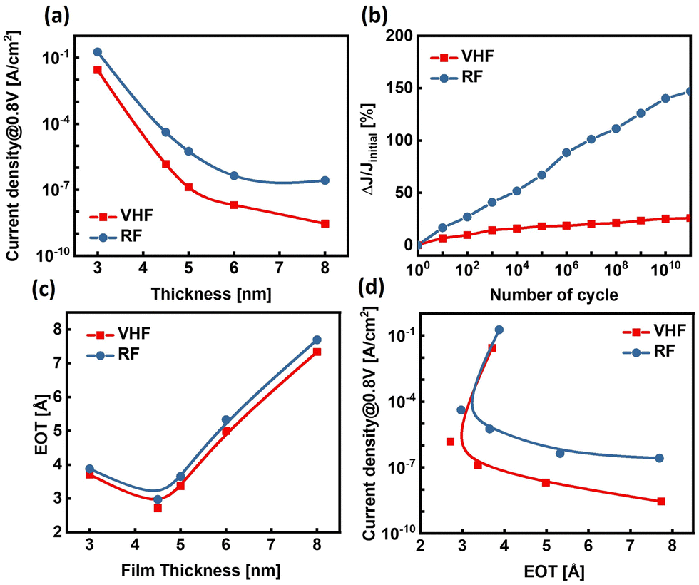 | ||
| Fig. 4 (a) Current density (J) vs. thickness comparison for the VHF and RF-deposited PE-ALD processed HZO films at room temperature. (b) Current density (J) change rate vs. electric field cycles for the VHF and RF-deposited HZO films at room temperature. (c) EOT comparison for the VHF and RF-deposited HZO films at various thicknesses(d) Current density (J) vs. EOT comparison for the VHF and RF-deposited HZO films at room temperature. | ||
In DRAM applications, the equivalent oxide thickness (EOT) is a crucial parameter for evaluating dielectric performance. VHF-deposited HZO consistently achieves a lower EOT compared to RF-deposited HZO across various film thicknesses, emphasizing its enhanced scalability (Fig. 4c). When comparing leakage current and EOT, VHF-deposited HZO outperforms RF-deposited HZO by at least an order of magnitude at the same EOT, underscoring the promise of VHF-deposited HZO for advanced DRAM applications, where both low leakage current and minimal EOT are critical (Fig. 4d).
From the current-lifetime data, the Weibull distribution for VHF-deposited HZO films was derived, as shown in Fig. 5a. The measured lifetimes of VHF-deposited HZO were 103 s at 2.5 V, 102 s at 2.6 V, and 10 s at 2.7 V. Further analysis allowed for the estimation of the time-dependent dielectric breakdown (TDDB) voltage, VTDDB, at 2.35 V for a projected ten-year lifetime, which aligns well with the requirements of DRAM technology.
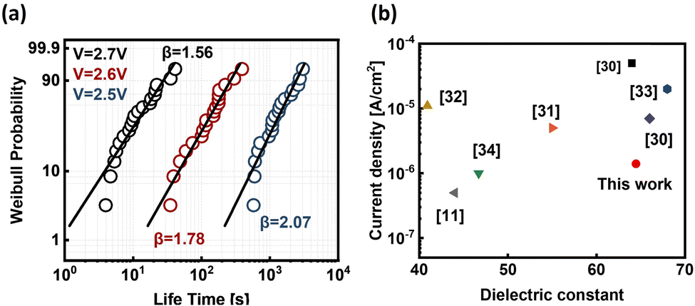 | ||
| Fig. 5 (a) Weibull distribution of VHF-deposited HZO extracted the Weibull slope (β) for three stress conditions. (b) Current density and dielectric constant of VHF-deposited HZO films compared to hafnium-based films (thickness < 8 nm) from previous studies. | ||
Fig. 5b provides a comparison of the dielectric constant and current density of VHF-deposited HZO films against data from previous studies11,30–34 VHF-deposited HZO demonstrates a significantly higher dielectric constant and a leakage current density that is an order of magnitude lower than reference values. This improvement in electrical performance is attributed to the VHF PE-ALD process, which results in lower average plasma ion bombardment energy and consequently reduces plasma-induced damage to the films. These enhancements highlight the promise of VHF-deposited HZO films for reliable, high-performance DRAM applications, where low leakage and long-term stability are essential.
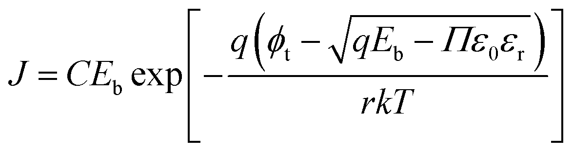
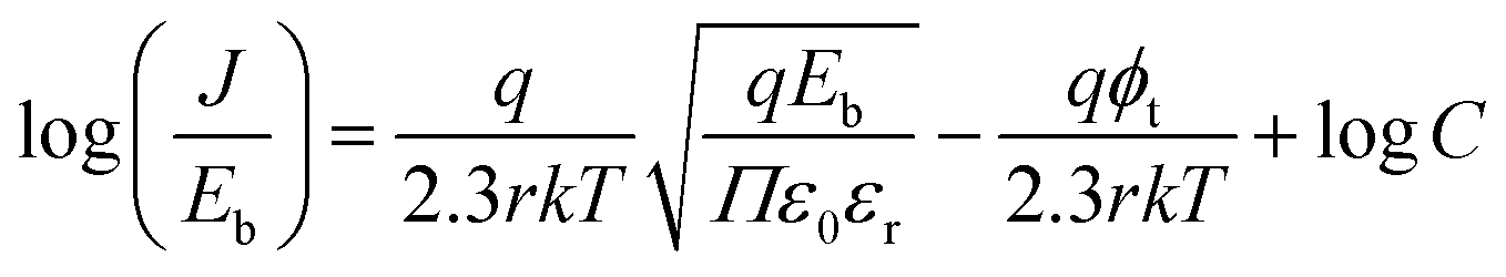
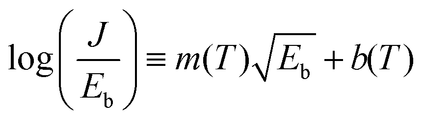
The current–voltage (J–V) characteristics of both VHF and RF-deposited HZO capacitors were analyzed over the temperature range of 298–373 K to evaluate their conduction mechanisms, as depicted in Fig. 6a and d. The results suggest that the Poole–Frenkel (PF) emission model effectively describes the conduction behavior in both types of capacitors. This model is instrumental in determining the trap depth (ϕt), which is directly related to the defect density within the dielectric material.35,36Fig. 6b and e present the fitting results of ln(J/Eb) vs.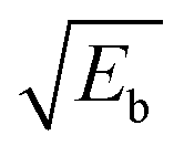 in the positive bias region, based on the PF emission analysis. In the PF emission model, the leakage current density (J) is governed by eqn (1):
 | (1) |
 | (2) |
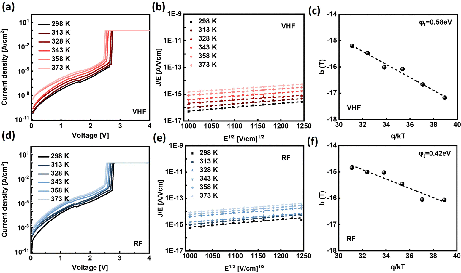 | ||
| Fig. 6 Trap states energy level of VHF and RF-deposited 4.5 nm HZO (Hf:Zr = 1:1) films. Evaluation of current–voltage–temperature (I–V–T) responses for VHF (a) and RF-deposited (d) 4.5 nm HZO (Hf:Zr = 1:1) films. Poole–Frenkel analysis of reverse leakage current for VHF-deposited HZO films (b) and RF-deposited 4.5 nm HZO (Hf:Zr = 1:1) films (e). The b(T) curves plotted against q/kT for VHF-deposited 4.5 nm HZO (Hf:Zr = 1:1) films (c) and RF-deposited 4.5 nm HZO (Hf:Zr = 1:1) films (f). | ||
where
 | (3) |
 | (4) |
 | (5) |
4. Conclusion
This study highlights the significant advantages of VHF PE-ALD in fabricating high-performance HZO films for DRAM applications, demonstrating superior results compared to conventional RF PE-ALD. VHF-deposited HZO films exhibit remarkable dielectric properties, achieving a dielectric constant of 64.47 at room temperature and peaking at 69.9 at elevated temperatures, nearing the theoretical limit of the tetragonal phase. These impressive values underscore the potential of VHF-deposited HZO for high-capacitance memory applications. Additionally, VHF-deposited HZO films demonstrate exceptionally low leakage currents, with a leakage current density of 1.47 × 10⁻⁶ A cm−2 at 0.8 V for films with a thickness of 4.5 nm—representing a 10-fold reduction compared to RF-deposited HZO films. This substantial improvement makes VHF-deposited HZO highly suitable for energy-efficient DRAM operations. The films also exhibit enhanced durability, showing minimal dielectric degradation under cycling stress and a notable reduction in the wake-up effect, attributed to the reduced defect formation during the deposition process. The equivalent oxide thickness (EOT) of VHF-deposited HZO across various film thicknesses further illustrates the scalability and integration potential of VHF PE-ALD in DRAM technology. Moreover, the presence of deep trap states at 0.58 eV below the conduction band in VHF-deposited HZO films indicates a lower defect density compared to RF-deposited films. This reduced defect density is a direct result of the minimized ion bombardment energy in VHF plasma, which decreases deposition-induced damage and enhances the structural integrity and reliability of the films. Overall, these findings establish VHF PE-ALD as a superior and promising technique for achieving high-κ, low-leakage HZO films that satisfy the rigorous demands of next-generation DRAM technology. This study paves the way for the continued optimization of ferroelectric VHF-deposited HZO films, offering a viable path forward for advanced semiconductor memory applications.Author contributions
The manuscript was written through contributions of all authors. All authors have given approval to the final version of the manuscript.Data availability
The data supporting this article have been included as part of the ESI.†Conflicts of interest
There are no conflicts of interest to declare.Acknowledgements
This work was supported by the National Research Foundation of Korea (No. 2021R1A2C2095322), MOTIE, Korea (RS-2024-00231985, RS-2024-00235655), and MSIT, Korea (RS-2024-00260527).References
- J. Muller, T. S. Boscke, U. Schroder, S. Mueller, D. Brauhaus, U. Bottger, L. Frey and T. Mikolajick, Nano Lett., 2012, 12, 4318–4323 CrossRef PubMed.
- J. Lee, K. Yang, J. Y. Kwon, J. E. Kim, D. I. Han, D. H. Lee, J. H. Yoon and M. H. Park, Nano Convergence, 2023, 10, 55 CrossRef CAS PubMed.
- M. Hellenbrand and J. MacManus-Driscoll, Nano Convergence, 2023, 10, 44 CrossRef CAS PubMed.
- L. Grenouillet, T. Francois, J. Coignus, S. Kerdiles, N. Vaxelaire, C. Carabasse, F. Mehmood, S. Chevalliez, C. Pellissier and F. Triozon, 2020 IEEE Symposium on VLSI Technology, IEEE, 2020, pp. 1–2 Search PubMed.
- K. Tahara, K. Toprasertpong, Y. Hikosaka, K. Nakamura, H. Saito, M. Takenaka and S. Takagi, 2021 Symposium on VLSI Technology, IEEE, 2021, pp. 1–2 Search PubMed.
- P. Pavan, R. Bez, P. Olivo and E. Zanoni, Proc. IEEE, 1997, 85, 1248–1271 CrossRef CAS.
- R. Bez, E. Camerlenghi, A. Modelli and A. Visconti, Proc. IEEE, 2003, 91, 489–502 CrossRef.
- M. H. Park, Y. H. Lee, H. J. Kim, Y. J. Kim, T. Moon, K. D. Kim, S. D. Hyun and C. S. Hwang, ACS Appl. Mater. Interfaces, 2018, 10, 42666–42673 CrossRef CAS PubMed.
- D. Das and S. Jeon, IEEE Trans. Electron Devices, 2020, 67, 2489–2494 CAS.
- M. Jung, V. Gaddam and S. Jeon, Nano Convergence, 2022, 9, 44 CrossRef CAS PubMed.
- S. Kim, S. H. Lee, M. J. Kim, W. S. Hwang, H. S. Jin and B. J. Cho, IEEE Electron Device Lett., 2021, 42, 517–520 CAS.
- Y. Qi, X. Xu, I. Krylov and M. Eizenberg, Appl. Phys. Lett., 2021, 118 Search PubMed.
- N. Manikanthababu, T. Basu, S. Vajandar, S. Nageswara Rao, B. Panigrahi, T. Osipowicz and A. Pathak, J. Mater. Sci.: Mater. Electron., 2020, 31, 3312–3322 CrossRef CAS.
- A. Yanguas-Gil, Growth and Transport in Nanostructured Materials: Reactive Transport in PVD, CVD, and ALD, Springer, 2016 Search PubMed.
- D. Munoz-Rojas, T. Maindron, A. Esteve, F. Piallat, J. Kools and J.-M. Decams, Mater. Today Chem., 2019, 12, 96–120 CrossRef CAS.
- M. Leskelä and M. Ritala, Thin Solid Films, 2002, 409, 138–146 CrossRef.
- S.-J. Park, J.-P. Lee, J. S. Jang, H. Rhu, H. Yu, B. Y. You, C. S. Kim, K. J. Kim, Y. J. Cho and S. Baik, Nanotechnology, 2013, 24, 295202 CrossRef PubMed.
- R. D. Clark, Materials, 2014, 7, 2913–2944 CrossRef PubMed.
- S. Bothra, C. T. Gabriel, S. Lassig and D. Pirkle, J. Electrochem. Soc., 1995, 142, L208 CrossRef CAS.
- K. P. Cheung and C.-S. Pai, IEEE Electron Device Lett., 1995, 16, 220–222 Search PubMed.
- T. Ando, Materials, 2012, 5, 478–500 CrossRef CAS PubMed.
- J. Byun, Y. Ji, K. Kim, K. Kim, H. Tak, A. R. Ellingboe and G. Y. Yeom, Nanotechnology, 2020, 32, 075706 CrossRef PubMed.
- Y. J. Ji, H. I. Kim, K. H. Kim, J. E. Kang, D. San Kim, K. S. Kim, A. Ellingboe, D. W. Kim and G. Y. Yeom, Surf. Interfaces, 2022, 33, 102219 CrossRef CAS.
- A. Kosarev, A. Smirnov, A. Abramov, A. Vinogradov, A. Y. Ustavschikov and M. Shutov, J. Vac. Sci. Technol., A, 1997, 15, 298–306 CrossRef CAS.
- H. Takatsuka, M. Noda, Y. Yonekura, Y. Takeuchi and Y. Yamauchi, Sol. Energy, 2004, 77, 951–960 CrossRef CAS.
- X.-M. Zhu, W.-C. Chen, S. Zhang, Z.-G. Guo, D.-W. Hu and Y.-K. Pu, J. Phys. D: Appl. Phys., 2007, 40, 7019 CrossRef CAS.
- K. Yang, M. Jung, T. Jung, J. S. Yoon, J. Hwang, H. Shin, S. Kim, C. Kim and S. Jeon, ACS Appl. Electron. Mater., 2024, 6, 5067–5076 CrossRef CAS.
- H. J. Kim, M. H. Park, Y. J. Kim, Y. H. Lee, T. Moon, K. Do Kim, S. D. Hyun and C. S. Hwang, Nanoscale, 2016, 8, 1383–1389 RSC.
- P. Jiang, Q. Luo, X. Xu, T. Gong, P. Yuan, Y. Wang, Z. Gao, W. Wei, L. Tai and H. Lv, Adv. Electron. Mater., 2021, 7, 2000728 CrossRef CAS.
- V. Gaddam, J. Hwang, H. Shin, C. Kim, G. Kim, H.-J. Kim, J. Lee, H.-C. Kim, B. Park and S. Lim, Low-Damage Processed and High-Pressure Annealed High-k Hafnium Zirconium Oxide Capacitors near Morphotropic Phase Boundary with Record-Low EOT of 2.4 Å & high-k of 70 for DRAM Technology, 2024 IEEE Symposium on VLSI Technology and Circuits, 2024 DOI:10.1109/VLSITechnologyandCir46783.2024.10631348.
- S. Oh, H. Jang and H. Hwang, IEEE Electron Device Lett., 2023, 45, 28–31 Search PubMed.
- J. Y. Kim, S. H. Park, Y. J. Kim, J. H. Kim, S. K. Choi, H. R. Kwon, Y. J. Lee, S. J. Kim, D. Shin and B. Yeo, ACS Appl. Mater. Interfaces, 2024, 16, 60811–60818 CrossRef CAS PubMed.
- J. Zhou, Y. Kang, X. Wang, Z. Zhou, H. Ni, L. Jiao, Z. Zheng and X. Gong, J. Phys. D: Appl. Phys., 2021, 55, 014003 CrossRef.
- Z. Luo, X. Du, H. Gan, Y. Lin, W. Yan, S. Shen, Y. Yin and X. Li, Appl. Phys. Lett., 2023, 122, 192903 CrossRef CAS.
- J. G. Simmons, Phys. Rev., 1967, 155, 657 CrossRef CAS.
- J. Yeargan and H. Taylor, J. Appl. Phys., 1968, 39, 5600–5604 CrossRef CAS.
- X. Lu, C. Liu, H. Jiang, X. Zou, A. Zhang and K. M. Lau, Appl. Phys. Express, 2016, 9, 031001 CrossRef.
Footnote |
| † Electronic supplementary information (ESI) available. See DOI: https://doi.org/10.1039/d4tc04979a |
| This journal is © The Royal Society of Chemistry 2025 |