
 Open Access Article
 This Open Access Article is licensed under a Creative Commons Attribution-Non Commercial 3.0 Unported Licence
Photo-response performance regulation of a type-Ib diamond-based photodetector by H2 annealing and ozone treatment†
Keyun
Gu
 ab,
Zilong
Zhang
b,
Takeo
Ohsawa
b,
Masataka
Imura
b,
Jian
Huang
*a,
Yasuo
Koide
b and
Meiyong
Liao
*b
ab,
Zilong
Zhang
b,
Takeo
Ohsawa
b,
Masataka
Imura
b,
Jian
Huang
*a,
Yasuo
Koide
b and
Meiyong
Liao
*b
aSchool of Materials Science and Engineering, Shanghai University, Shanghai 200444, P. R. China. E-mail: jianhuang@shu.edu.cn
bResearch Center for Functional Materials, National Institute for Materials Science (NIMS), Namiki 1-1, Tsukuba, Ibaraki 305-0044, Japan. E-mail: meiyong.liao@nims.go.jp
First published on 13th February 2025
Abstract
Deep ultraviolet (DUV) photodetectors (PDs) based on ultra-wide bandgap semiconductor diamond-based have attracted extensive attention due to the immunity to solar light on the earth and thermal stability in extremely harsh environments. However, the preparation of a high-quality and high-purity single-crystal diamond epilayer remains a major obstacle to achieve high photo-response performance. Here, we demonstrate that diamond PDs with tunable photoresponse properties can be obtained on type-Ib diamonds through simple annealing in ambient H2 and a surface ozone treatment process. The surface holes and the nitrogen defects inside the type-Ib diamond work together to regulate the overall photoresponse performance. The responsivity of the PDs can be adjusted from 84.3 A W−1 to 2.65 × 10⁴ A W−1, and the response time can be modulated from 42.5 s to less than 240 ms. The achievement of photo response performance modulation of PDs originates from the cooperative effect of deep natural nitrogen defects and surface states. Thus, our findings provide an alternative method and facile strategy for the tailoring of PDs’ performance, which can meet different application requirements.
Introduction
A solar-blind deep-ultraviolet (DUV) photodetector exhibits excellent spectral selectivity since it responds to light with wavelengths shorter than 280 nm, which is almost non-existent in the earth's atmosphere.1–3 The extremely low noise interference from the environment enables high-accuracy detection of solar-blind DUV light. Thus, solar-blind DUV PDs are in demand for applications covering intersatellite secure communications,4 DUV imaging,5 and environmental monitoring and analysis.6–8 Diamond is a single-element ultra-wide bandgap (5.5 eV) semiconductor, which has an excellent thermally and chemically stable structure, the highest thermal conductivity (22 W cm−1 K−1), and a large breakdown field >10 MV cm−1.9–12 Compared with multi-element compound semiconductors, such as AlGaN, Ga2O3, and MgZnO, diamond does not have problems such as component segregation or oxygen vacancies.13–16 Besides, diamond has high radiation resistance.17 Furthermore, diamond can achieve high sensitivity to DUV light, but weak response to visible light, making it an extremely attractive material for preparing solar-blind DUV PDs.The initial efforts in developing diamond PDs were mainly on polycrystalline diamond. In 1993, Binari et al. fabricated a metal–semiconductor–metal (MSM) PD based on polycrystalline diamond, which showed a quantum efficiency of 39% at 400 V bias voltage and under a wavelength of 200 nm.18 In 1998, Jiang et al. demonstrated an MSM PD based on diamond thin film grown on a silicon substrate, which achieved a low operating voltage around 5 V.19 In 2005, we investigated the performance of a PD based on boron (B)-doped homoepitaxial single-crystal diamond (SCD), which showed a high ultraviolet photocurrent at 220 nm (seven orders of magnitude higher than dark current) and a high spectral selectivity (DUV/visible rejection ratio of 106).20 Lin et al. developed SCD MSM PDs, which showed a responsivity of 21.8 A W−1 and a detectivity of 1.39 × 1012 cm Hz1/2 W−1 at 218 nm light.21 A responsivity of 524.9 A W−1 was later achieved by treating the SCD epitaxial layer with hydrogen plasma and optimizing the Schottky barrier with an electrode contact.22 To date, almost all high-performance diamond-based solar blind DUV PDs rely on high-quality epitaxial layers. Recently, we showed an EQE of 9.41 × 10⁶% for the diamond DUV PDs by simply treating a type-Ib diamond substrate using hydrogen plasma treatment.23 Regardless of the growth of high-quality epitaxial layers or hydrogen plasma treatment, MPCVD equipment was used in our previous work.
In this work, we report the development of DUV detectors by simply annealing type-Ib diamond substrates in an ambient H2. By combining with UV/ozone treatment, the overall response properties such as the DUV responsivity, response speed, dark current, and spectral response of the diamond PDs can be regulated. The responsivity (R) of the PD based on hydrogen-annealed diamond is up to 2.65 × 10⁴ A W−1, corresponding to an ultrahigh external quantum efficiency (EQE) of 1.50 × 10⁷% but a lower response speed. After UV/ozone treatment, the device response time can be as short as less than 240 ms. The modulation of the photoresponse properties of the H-annealed type-Ib diamond is resulted from the cooperative effect of the nitrogen impurity in diamond and the surface states. These findings provide a simple and effective strategy for fabricating diamond DUV PDs, which can meet different application requirements.
Results and discussion
Material characterization
The surface morphology of the H2 annealed type-Ib diamond substrate scanned by AFM is shown in Fig. 1(a1) and (a2). It can be seen that the surface of diamond is smooth without large bulges or damage after H2 annealing. The root mean square (RMS) is extremely low (∼0.04 nm). Fig. 1(b1 and b2) display the 2D mapping of the Raman peak full width at half maximum (FWHM) of an area of 30 × 30 μm2 and the statistical histogram, respectively. The Raman peak position is around 1332.23 cm−1, which is close to the standard value of 1332.5 cm−1. The FWHM is evenly distributed, and the average FWHM is around 2.1 cm−1. Based on the XPS analysis shown in Fig. 1(c1) and (c2), for hydrogen annealed diamond, the C–C sp3 components account for 96.3% and C–O accounts for 3.7%. The peak of C–O is attributed to the surface adsorbed carbon oxides when exposed in ambient air.24,25 After 10 min ozone treatment, the content of C–O increases to 5.87%, indicating that its surface gradually changes from hydrogen terminal to oxygen terminal. Furthermore, the sp3 C–C peak of ozone treated diamond shifts from 282.25 eV to 283.96 eV, which can be explained by the difference of band bending.26,27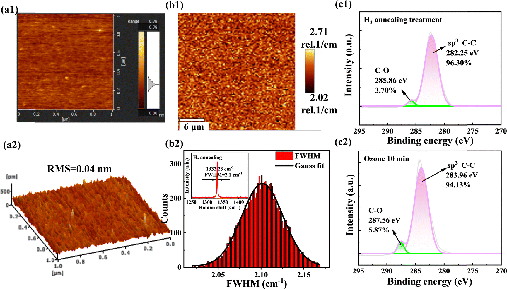 | ||
| Fig. 1 (a1) and (a2) 2 dimensional (D) and 3D surface morphology of H2 annealed diamond. (b1) and (b2) Raman imaging of an area of 30 × 30 μm2, and statistical distribution of the Raman FWHM of the H2 annealed diamond. (c1) and (c2) X-ray photoelectron spectroscopy (XPS) spectra of H2 annealed and 10 min ozone-treated diamond. | ||
Photoresponse property regulation
The surface electrical conductivity of H-terminated diamond can be enhanced by hydrogen annealing. Taking into account that the bulk type-Ib diamond contains a large amount of nitrogen (N) around 1019 cm−3, the surface electrical conductivity caused by two-dimensional hole gas (2DHG) is decayed because of the depletion of partial surface holes due to N trapping, which is similar to hydrogen plasma treated surfaces. The as-annealed diamond-based PD has a dark current around 2.37 × 10⁻⁵ A at 5 V, as shown in Fig. 2(a). This value is two orders of magnitude lower than that of “intrinsic” diamond with surface H-termination.28 The dark current of the PD ozone treated for 5 minutes is reduced around 3.82 × 10⁻⁸ A, and that of the PD ozone treated for 10 minutes is around 1.75 × 10⁻⁹ A, as depicted in Fig. 2(b) and (c), respectively. Under 220 nm DUV light illumination, the photocurrent of three PDs is enhanced to 1.10 × 10⁻⁴ A, 3.51 × 10⁻⁶ A, and 2.76 × 10⁻⁷ A, respectively, illustrating a sensitive response to DUV light. The PD's dark current and photocurrent gradually decrease with prolonged ozone treatment durations (Fig. 2(d)), resulting from the decrease of the 2DHG concentration. And the ratio of photocurrent to dark current (PDCR) of the PDs increases with the ozone treatment time.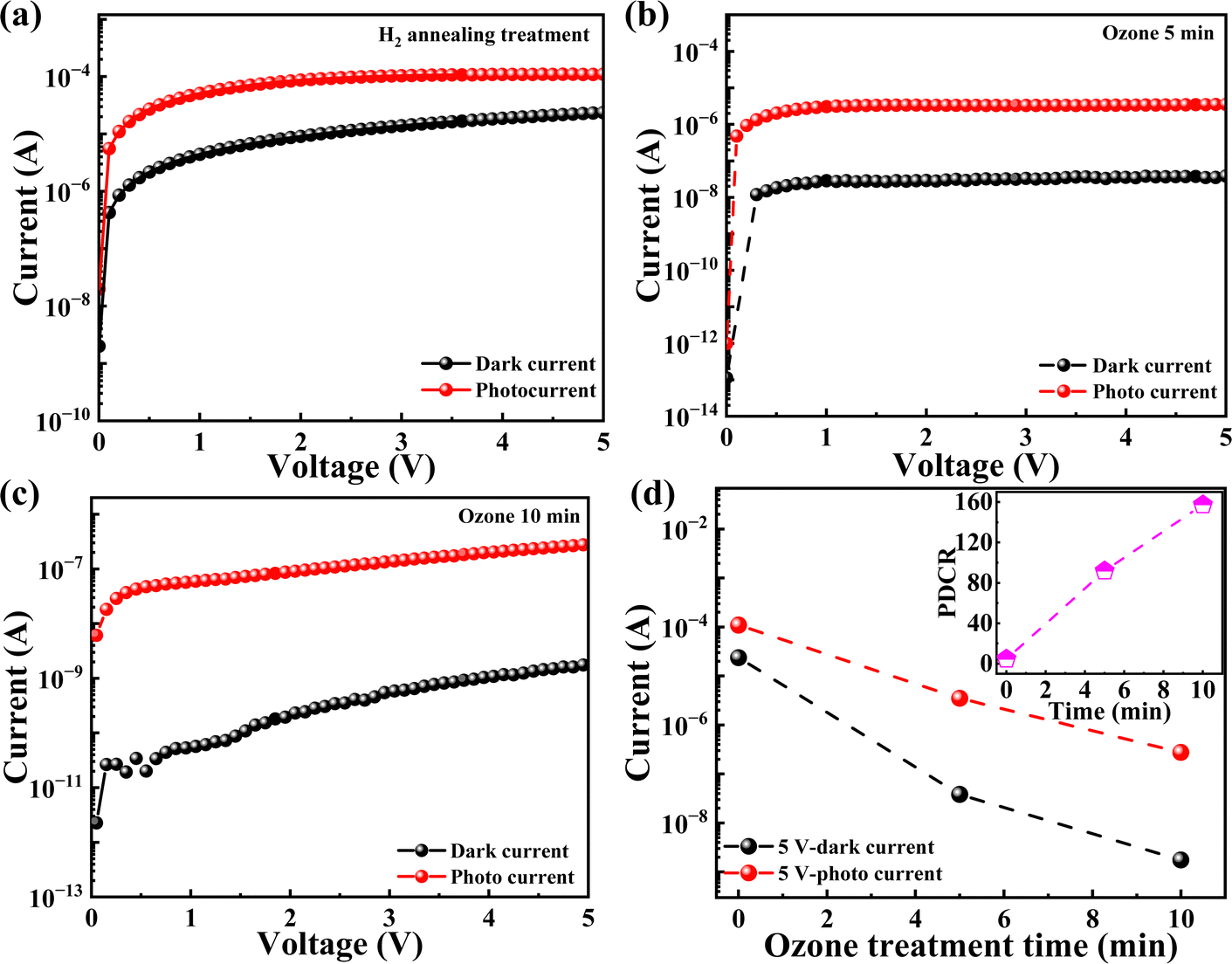 | ||
| Fig. 2 I–V characteristics of the diamond PDs. (a) H2-annealed, (b) ozone treatment for 5 min, (c) ozone treatment for 10 min. (d) Dark and photo current vs. ozone treatment time. | ||
The responsivity (R) and external quantum efficiency, EQE, critical figures-of-merit in photodetectors, representing the ratio of extracted carriers and incident photons, are obtained under 5 V bias. The responsivity, R, is calculated according to:
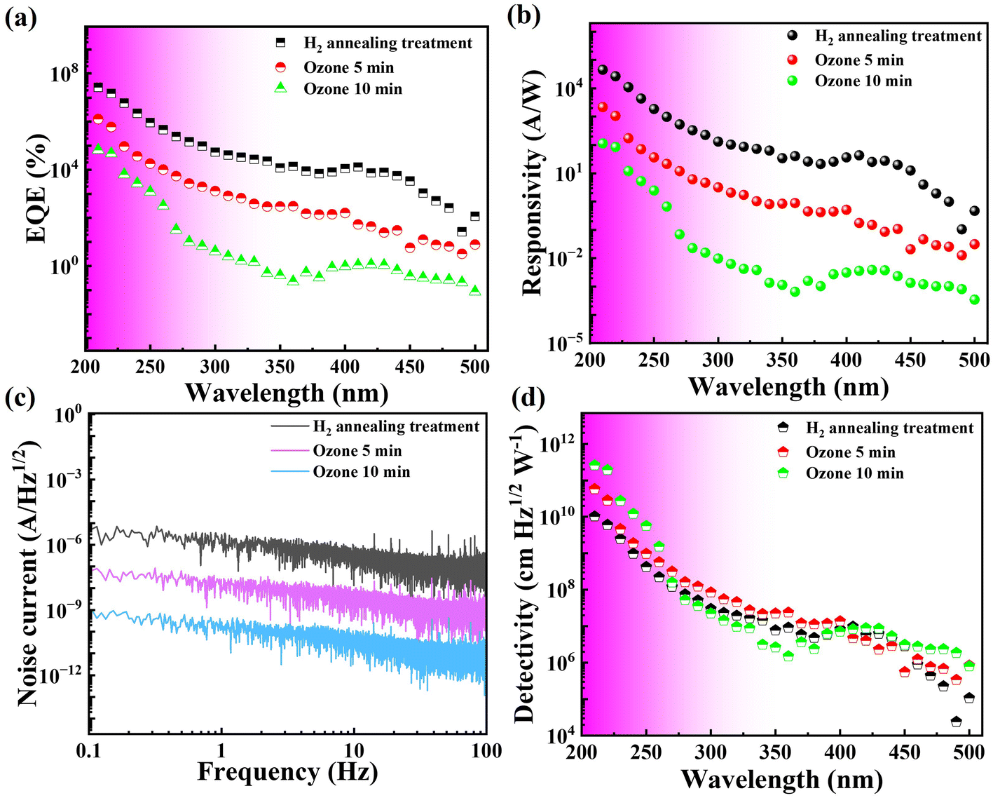 | ||
| Fig. 3 (a) The measured external quantum efficiency, EQE, (b) responsivity, R, (c) noise current, and (d) detectivity, D* of PDs. | ||
The noise currents of the H2 annealed PD, the 5 min ozone-treated PD, and the 10 min ozone-treated PD are 3.11 × 10⁻⁷ A Hz−1/2, 2.65 × 10⁻⁹ A Hz−1/2, and 3.09 × 10⁻¹¹ A Hz−1/2, respectively, as illustrated in Fig. 3(c). Based on the noise current, D* can be calculated to be 6.03 × 109 cm Hz1/2 W−1, 2.83 × 1010 cm Hz1/2 W−1, and 1.93 × 1011 cm Hz1/2 W−1 for the H2 annealed PD, the 5 min ozone-treated PD, and the 10 min ozone-treated PD, respectively, as shown in Fig. 3(d). The PD with 10 min ozone treatment has a higher D*, attributed to the lower noise current. And all PDs exhibit higher D* in the DUV region.
Furthermore, the response time including the rise time τr (10% to 90% of the maximum photocurrent) and the decay time τd (90% to 10% of the maximum photocurrent) were calculated. The τr and τd of H2 annealed PD are beyond 42 s (Fig. 4(a)), and the response time becomes shortened with the prolonging of the ozone time (Fig. 4(d)). The PDs with 5 min ozone and 10 min ozone treatment have the response time of τr/τd = 9.50 s/12.24 s, and τr/τd < 240 ms, respectively, as displayed in Fig. 4(b) and (c), respectively. The PDs show no current decay for cyclic switching, indicating that the PDs have good stability, as shown in Fig. S2 (ESI†). Furthermore, the photocurrent increases linearly with the incident power density.
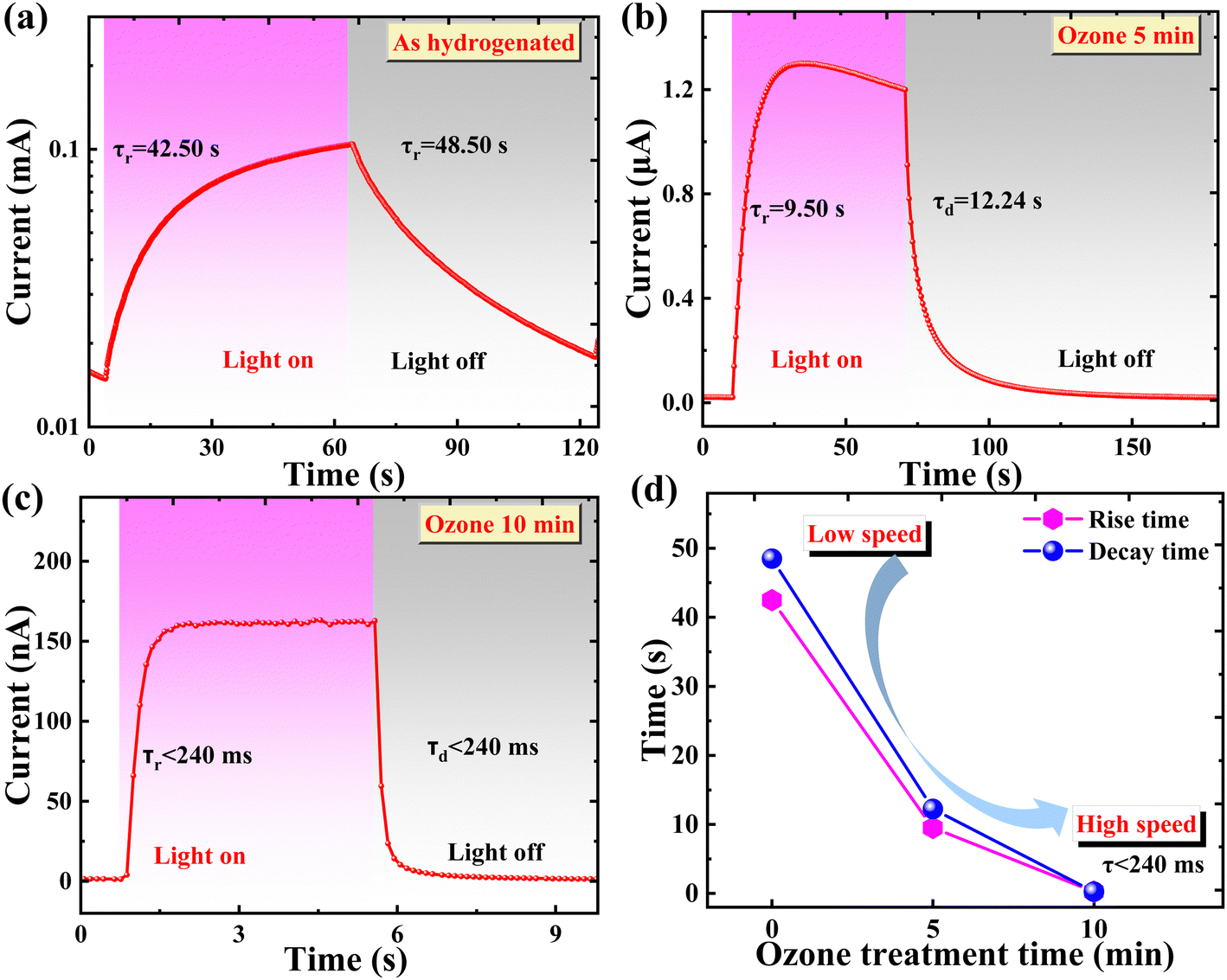 | ||
| Fig. 4 Time-dependent photo-response of PDs. (a) H2-annealed, (b) ozone-treated for 5 min and (c) ozone-treated for 10 min. (d) Response time vs. ozone treatment time. | ||
The key parameters including the dark current, R, EQE, and response time of diamond-based PDs in this work and previously reported work22,23,36–42 are summarized in Table 1. Almost all other reported diamond PDs in the table are based on epitaxial SCD layers prepared using the MPCVD method. Our other work23 demonstrated an EQE of 9.41 × 10⁶% by using MPCVD hydrogen plasma to treat a type-Ib diamond surface. In this work, we simply used H2 annealed commercial HPHT type-Ib diamond to achieve comparable ultrahigh responsivity (2.65 × 10⁴ A W−1) and external quantum efficiency (1.50 × 10⁷%). Furthermore, the PDs in this work operate with a voltage as low as 5 V and the response performance of the PDs can be tailored through surface treatments. The surface conductivities and photoresponse properties for the diamond surfaces either by hydrogen plasma treatment or thermal annealing in a hydrogen ambient are similar. The thermal stability of the diamond surfaces treated by these two methods is under investigation.
| Material | Structure | Dark current | Responsivity (A W−1) | EQE (%) | Response time (τr/τd) | Ref. |
|---|---|---|---|---|---|---|
| B-doped SCD | MSM | 10−12 A@30 V | 18@−23 V, 220 nm | 1.01 × 10⁴ | <10 ms | 36 |
| SCD | MSM | 1.12 × 10⁻¹² A@30 V | 0.20@30 V, 220 nm | 1.12 × 10² | 20 μs/1000 μs | 37 |
| Graphene-MCD | Heterojunction | 10−6 A cm−2 | 1.4@5 V, 220 nm | 7.9 × 10² | — | 38 |
| SCD | MSM | 10−12 A@30 V | 1.18@50 V, 210 nm | 6.66 × 10² | 640 ms/34 ms | 39 |
| SCD | MSM | 10−13 A@50 V | 0.11@7 V, 220 nm | 62.1 | – | 40 |
| SCD | MSM | 1.08 × 10⁻¹⁰ A@13 V | 524.9@13 V, 220 nm | 2.96 × 10⁵ | 0.16 μs/120 μs | 22 |
| SCD | MSM | 10−12 A@47 V | 0.013@47 V, 225 nm | 7.19 | 5 ns/20 ns | 41 |
| SCD | MSM | 10−12 A@30 V | 0.325@30 V, 210 nm | 1.92 × 10² | 1.2 ms | 42 |
| H-plasma treated Ib-diamond | MSM | 2.34 × 10⁻⁵ A@5 V | 1.6 × 10⁴ @5 V, 220 nm | 9.41 × 10⁶ | 30.4 s | 23 |
| H2 annealed Ib-diamond | MSM | 2.37 × 10⁻⁵ A@5 V | 2.65 × 10⁴@5 V, 220 nm | 1.50 × 10⁷ | 42.5 s/48.5 s | This work |
| Ozone 5 min Ib-diamond | MSM | 3.82 × 10⁻⁸ A@5 V | 1.06 × 10³@5 V, 220 nm | 6.00 × 10⁵ | 9.50 s/12.24 s | This work |
| Ozone 10 min Ib-diamond | MSM | 1.75 × 10⁻⁹ A@5 V | 84.3@5 V, 220 nm | 4.76 × 10⁴ | <240 ms | This work |
Photoresponse mechanism
Hydrogen-annealed type-Ib diamond shows a negative electron affinity (NEA) and exhibits surface conductivity due to the formation of two-dimensional hole gas on the surface.43–45 Thus, the energy band of H2 annealed diamond bends upwards. Furthermore, there are nitrogen defects inside the type Ib-diamond, which compensate surface holes and electrons and result in an increase in ionized N+ traps, as shown in Fig. 5(a). This results in the H2-annealed type-Ib diamond PD possessing lower dark current (2.37 × 10⁻⁵ A) than those of H-terminated intrinsic diamonds (∼mA).46,47 After ozone treatment, the surface conductivity and surface hole concentration decrease, the energy band bends upward slightly, and less nitrogen is ionized, as shown in Fig. 5(b) and (c). Under DUV light illumination, the electrons in the valence band are excited to the conduction band, and some of the electrons are captured by N+ traps, causing equivalent holes to accumulate near the surface and the energy band to bend upward more sharply, as shown in Fig. 5(d). This corresponds to the ultrahigh EQE (1.50 × 10⁷%) and responsivity (2.65 × 10⁴ A W−1). While the regulation process of more N+ traps slows down the overall carrier recombination process, the response time of the H2-annealed type-Ib diamond PD is longer (τr/τd = 42.50 s/48.50 s). As the UV/ozone treatment time increases, surface holes and N+ traps decrease, as depicted in Fig. 5(e) and (f), resulting in a lower EQE of 6.00 × 10⁵% and 4.76 × 10⁴%, respectively for the 5 min and 10 min ozone-treated PDs. And the carrier recombination gradually changes from being dominated by N+ traps to being dominated by band-to-band. Therefore, the response speed accelerates (τr/τd < 240 ms for 10 min ozone-treated PD).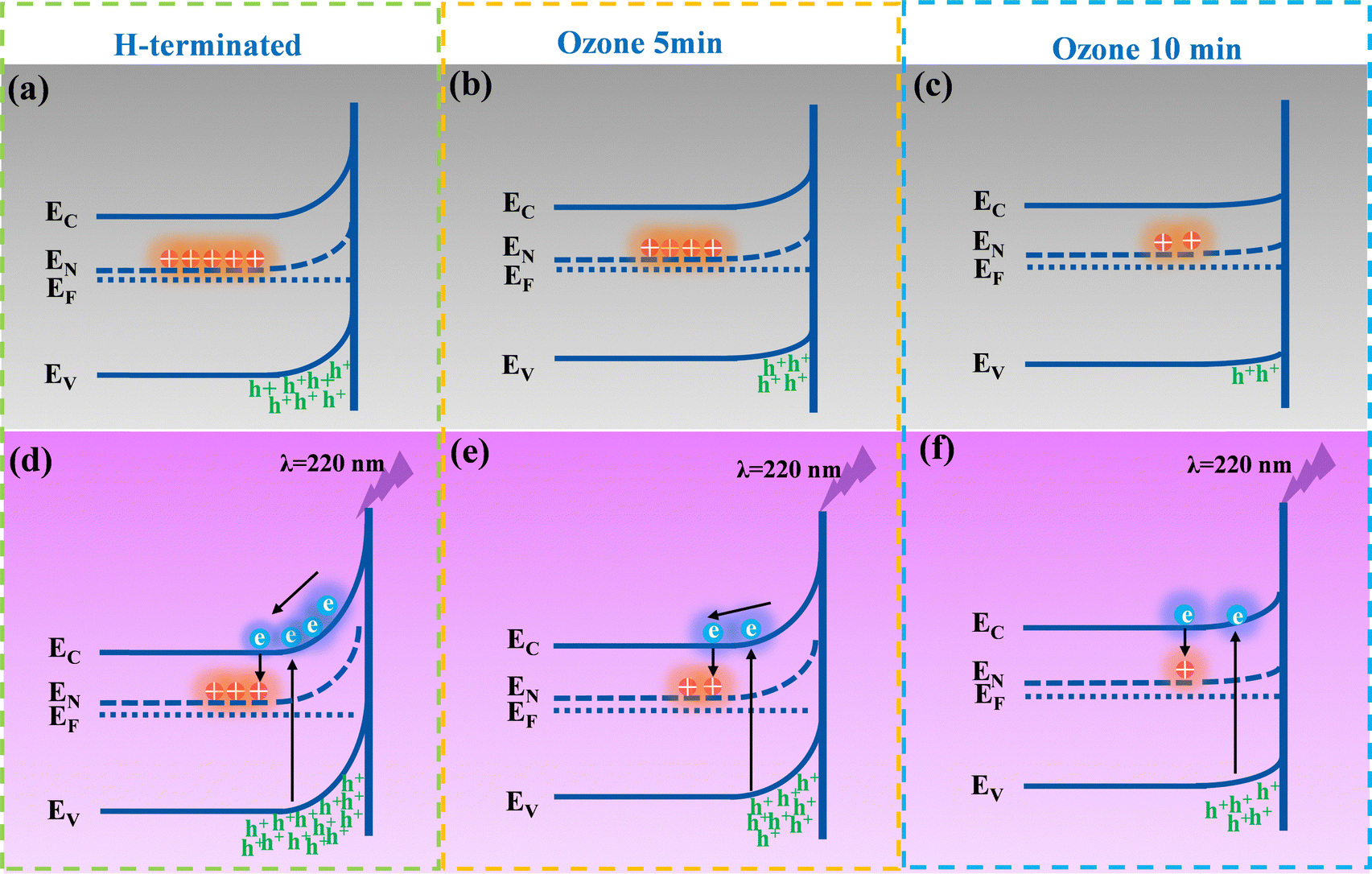 | ||
| Fig. 5 Energy band diagrams of H2-annealed, ozone-treated 5 min, and ozone-treated 10 min PDs: (a)–(c) in the dark condition and (d)–(f) under 220 nm UV light. | ||
Experimental
The type Ib-type diamond with the dimensions of 2.5 mm × 2.5 mm × 0.5 mm was cleaned ultrasonically in acetone, absolute ethanol, and deionized water for 5 minutes, respectively. Before annealing in ambient H2, the diamond substrate was boiled in an acid mixture of H2SO4 and HNO3. The overall experimental treatment route is shown in Fig. 6. The cleaned diamond was transferred to a high-vacuum chamber, which has a base pressure of 10−7 Torr. The annealing temperature, the pressure, and the duration were 860 °C, 80 Torr, and 1 h, respectively. The Ti/Au interdigitated electrodes with a finger width of 10 μm were deposited on a hydrogen annealed diamond surface. The optically active receiving area is around 5 × 10⁻⁴ cm2. The as-annealed PDs were placed into a UV/ozone reaction chamber for 5 min and 10 min treatments. The optical image of the PD is shown in Fig. S1 (ESI†). The diamond surface morphology and root mean square were characterized by atomic force microscopy (AFM). The Raman spectrometer with a 532 nm laser was used to measure the crystal quality of the as-annealed diamond. A commercial X-ray photoelectron spectrometer (XPS, Thermo Fisher Scientific, Japan) was used to measure the binding states of the surface composition. The overall photoelectric performance of the PDs was measured by using a Keithly2400 semiconductor Analyzer and an Ushio Xenon lamp combined with an Acton monochromator with order sorting filters and a standard lock-in amplifier technique. The power density of the 220 nm incident light is around 6.5 μW cm−2.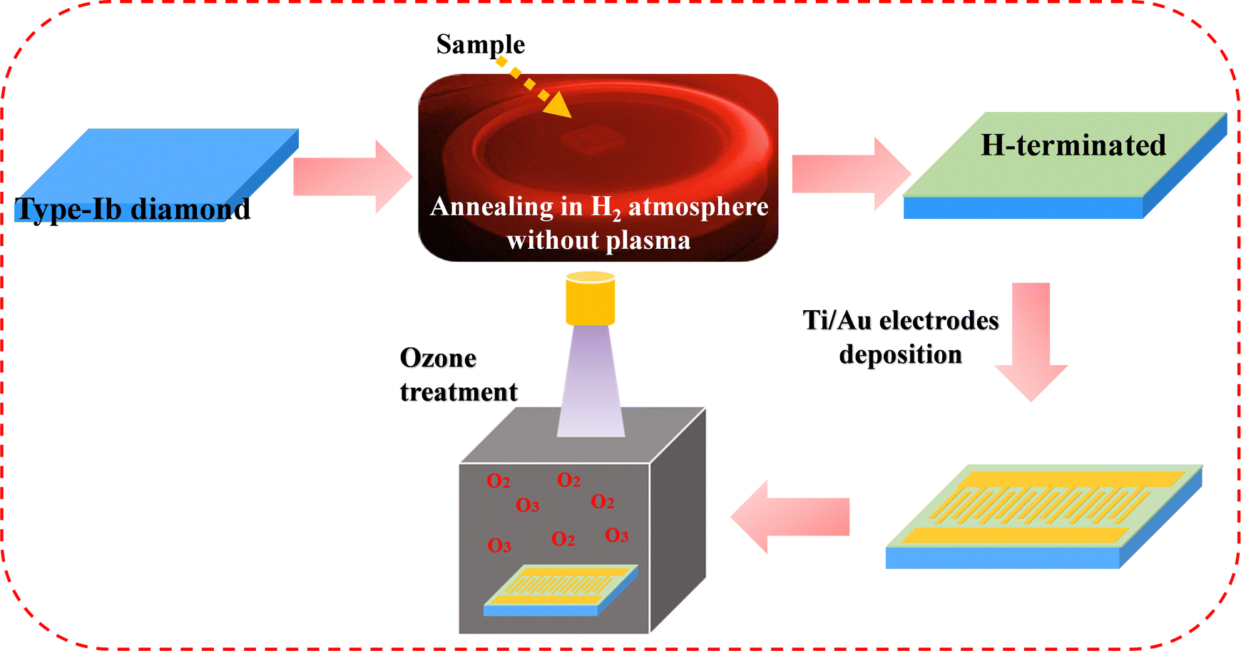 | ||
| Fig. 6 Schematic diagrams of the experimental treatment route. | ||
Conclusions
In conclusion, a high-temperature annealing procedure in ambient H2 was conducted to fabricate a H-terminated type-Ib diamond-based PD. The surface characteristics and the overall photoresponse performance of H2 annealed type-Ib diamond are comparable with those of hydrogen plasma-treated type-Ib diamond. The UV/ozone surface treatment regulated the photoresponse performance through the cooperation of surface states and the natural doped nitrogen in type Ib diamond. The responsivity was modulated from 2.65 × 10⁴ A W−1 to 84.3 A W−1 and the response time from 42.5 s to <240 ms. These findings provide a simple and effective technique to fabricate DUV-PDs with tunable performance for different industrial applications.Data availability
The authors confirm that the data supporting this article have been included in the article or ESI.†Conflicts of interest
The authors declare that they have no conflict of interest.Acknowledgements
This work was supported by JSPS KAKENHI (Grant Number 24H00287, 22K18957, 20H02212), Bilateral joint research between JSPS/CAS, and Advanced Research Infrastructure for Materials and Nanotechnology in Japan (ARIM) of MEXT (JPMXP1223NM5297). Keyun Gu thanked the financial support from the China Scholarship Council (No. 202306890007).Notes and references
- X. Chen, K. Liu, Z. Zhang, C. Wang, B. Li, H. Zhao, D. Zhao and D. Shen, ACS Appl. Mater. Interfaces, 2016, 8, 4185–4191 CrossRef CAS PubMed
.
- T. Oshima, T. Okuno, N. Arai, N. Suzuki, H. Hino and S. Fujita, Jpn. J. Appl. Phys., 2009, 48, 011605 CrossRef
- Z. Zhang, C. Lin, X. Yang, Y. Tian, C. Gao, K. Li, J. Zang, X. Yang, L. Dong and C. Shan, Carbon, 2021, 173, 427–432 CrossRef CAS
- C. Lin, Y. Lu, Y. Tian, C. Gao, M. Fan, X. Yang, L. Dong and C. Shan, Opt. Express, 2019, 27, 29962–29971 CrossRef CAS PubMed
- Y. Chen, Y. Lu, C. Lin, Y. Tian, C. Gao, L. Dong and C. Shan, J. Mater. Chem. C, 2018, 6, 5727–5732 RSC
- J. Chen, W. Ouyang, W. Yang, J. H. He and X. Fang, Adv. Funct. Mater., 2020, 30, 1909909 CrossRef CAS
- C. Wu, F. Wu, C. Ma, S. Li, A. Liu, X. Yang, Y. Chen, J. Wang and D. Guo, Mater. Today Phys., 2022, 23, 100643 CrossRef CAS
- Q. Yuan, W. Wang, W. Zhang, M. Qiu, M. Yang, Z. Jia, B. Wang, C. Lin, K. Nishimura, K. Chang, K. Chee, J. Cui and N. Jiang, Functional Diamond, 2023, 3, 2256360 CrossRef
- M. Liao, L. Sang, H. Sun, T. Li and S. Koizumi, Appl. Phys. Lett., 2021, 119, 073504 CrossRef CAS
- M. Liao, Funct. Diam., 2021, 1, 29–46 CrossRef
- C. E. Nebel, Funct. Diam., 2023, 3, 2201592 CrossRef
- K. Gu, Z. Zhang, G. Chen, J. Huang, Y. Koide, S. Koizumi, W. Zhao and M. Liao, Carbon, 2024, 225, 119159 CrossRef CAS
- D. Guo, Q. Guo, Z. Chen, Z. Wu, P. Li and W. J. Tang, Mater. Today Phys., 2019, 11, 100157 CrossRef
- Y. Chen, Y. Lu, X. Yang, S. Li, K. Li, X. Chen, Z. Xu, J. Zang and C. Shan, Mater. Today Phys., 2021, 18, 100369 CrossRef CAS
- D. Thapa, J. Huso, K. Miklos, P. M. Wojcik, D. N. McIlroy, J. L. Morrison, C. Corolewski, M. D. McCluskey, T. J. Williams and M. Grant Norton, J. Mater. Sci.: Mater. Electron., 2017, 28, 2511–2520 CrossRef CAS
- F. C. Massabuau, S. L. Rhode, M. K. Horton, T. J. O’Hanlon, A. Kovács, M. S. Zielinski, M. J. Kappers, R. E. Dunin-Borkowski, C. J. Humphreys and R. A. Oliver, Nano Lett., 2017, 17, 4846–4852 CrossRef CAS PubMed
- J. Xu, J. Dai, F. Ren, Y. Wang, P. Wang, S. Xu, S. Wu, J. Lin, Y. Yang and D. Guo, Carbon, 2021, 182, 525–536 CrossRef CAS
- S. Binari, M. Marchywka, D. Koolbeck, H. Dietrich and D. Moses, Diam. Relat. Mater., 1993, 2, 1020–1023 CrossRef CAS
- W. Jiang, J. Ahn, F. Xu, C. Liaw, Y. Chan, Y. Zhou and Y.-L. Lam, Appl. Phys. Lett., 1998, 72, 1131–1133 CrossRef CAS
- J. Alvarez, M. Liao and Y. Koide, Appl. Phys. Lett., 2005, 87 Search PubMed
- C. N. Lin, Y. J. Lu, X. Yang, Y. Z. Tian, C. J. Gao, J. L. Sun, L. Dong, F. Zhong, W. D. Hu and C. X. Shan, Adv. Opt. Mater., 2018, 6, 1800068 CrossRef
- C. Lin, Z. Zhang, Y. Lu, X. Yang, Y. Zhang, X. Li, J. Zang, X. Pang, L. Dong and C. Shan, Carbon, 2022, 200, 510–516 CrossRef CAS
- K. Gu, Z. Zhang, G. Chen, L. Sang, J. Huang, Y. Koide and M. Liao, Ultrahigh Responsivity of Diamond-based Solar-blind Photodetectors Using Hydrogen Plasma Treatmen 19th IEEE NEMS, 2024, pp. 1–4.
- T. Hattori, T. Igarashi, M. Ohi and H. Yamagishi, Jpn. J. Appl. Phys., 1989, 28, L1436 CrossRef CAS
- M. Kubovic, M. Kasu, H. Kageshima, F. J. D. Maeda and R. Materials, Diam. Relat. Mater., 2010, 19, 889–893 CrossRef CAS
- D. Ballutaud, N. Simon, H. Girard, E. Rzepka and B. Bouchet-Fabre, Diam. Relat. Mater., 2006, 15, 716–719 CrossRef CAS
- M. Wang, N. Simon, G. Charrier, M. Bouttemy, A. Etcheberry, M. Li, R. Boukherroub and S. Szunerits, Electrochem. Commun., 2010, 12, 351–354 CrossRef CAS
- M. Yuanchen, R. Zeyang, Y. Shiqi, S. Kai, Z. Jinfeng, Y. Xiaoli, N. Xiuxiu, Z. Jincheng and H. Yue, Funct. Diam., 2023, 3, 2219687 CrossRef
- Y. Xu and Q. Lin, Appl. Phys. Rev., 2020, 7, 011315 CAS
- G. Zeng, M. Zhang, Y. Chen, X. Li, D. Chen, C. Shi, X. Zhao, N. Chen, T. Wang and D. Zhang, Mater. Today Phys., 2023, 33, 101042 CrossRef CAS
- Y. Qin, L. Li, X. Zhao, G. S. Tompa, H. Dong, G. Jian, Q. He, P. Tan, X. Hou and Z. Zhang, ACS Photonics, 2020, 7, 812–820 CrossRef CAS
- W. Kaiser and W. Bond, Phys. Rev., 1959, 115, 857 CrossRef CAS
- V. Ralchenko, S. Pimenov, V. Konov, A. Khomich, A. Saveliev, A. Popovich, I. Vlasov, E. Zavedeev, A. Bozhko, E. Loubnin and R. Khmelnitskii, Diam. Relat. Mater., 2007, 16, 2067–2073 CrossRef CAS
- Y. Fang, F. Guo, Z. Xiao and J. Huang, Adv. Opt. Mater., 2014, 2, 348–353 CrossRef CAS
- C. Bao, Z. Chen, Y. Fang, H. Wei, Y. Deng, X. Xiao, L. Li and J. Huang, Adv. Mater., 2017, 29, 1703209 CrossRef PubMed
- M. Liao, Y. Koide and J. Alvarez, Appl. Phys. Lett., 2007, 90, 123507 CrossRef
- Z. Liu, F. Li, S. Li, C. Hu, W. Wang, F. Wang, F. Lin and H. Wang, Fabrication of UV photodetector on TiO2/diamond film, Sci. Rep., 2015, 5(1), 14420 CrossRef CAS PubMed
- M. Wei, K. Yao, Y. Liu, C. Yang, X. Zang and L. Lin, A solar-blind UV detector based on graphene-microcrystalline diamond heterojunctions, Small, 2017, 13(34), 1701328 CrossRef PubMed
- Z. Liu, D. Zhao, J. Ao, X. Chang, Y. Wang, J. Fu, M. Zhang and H. Wang, Responsivity improvement of Ti–diamond–Ti structured UV photodetector through photocurrent gain, Opt. Express, 2018, 26(13), 17092–17098 CrossRef CAS PubMed
- T. Teraji, S. Yoshizaki, H. Wada, M. Hamada and T. Ito, Highly sensitive UV photodetectors fabricated using high-quality single-crystalline CVD diamond films, Diam. Relat. Mater., 2004, 13(4–8), 858–862 CrossRef CAS
- M. Girolami, V. Serpente, M. Mastellone, M. Tardocchi, M. Rebai, Q. Xiu, J. Liu, Z. Sun, Y. Zhao and V. Valentini, Carbon, 2022, 189, 27–36 CrossRef CAS
- Y. Iwakaji, M. Kanasugi, O. Maida and T. Ito, Appl. Phys. Lett., 2009, 94, 223511 CrossRef
- P. Zhang, S. Zhang, W. Chen, S. Yan, W. Ma and H. Wang, Coatings, 2020, 10, 876 CrossRef CAS
- V. Seshan, D. Ullien, A. Castellanos-Gomez, S. Sachdeva, D. Murthy, T. Savenije, H. A. Ahmad, T. Nunney, S. Janssens and K. Haenen, J. Chem. Phys., 2013, 138, 234707 CrossRef CAS PubMed
- K. Gu, K. Wu, Z. Zhang, T. Ohsawa, J. Huang, Y. Koide, M. Toda and M. Liao, Adv. Funct. Mater., 2024, 2420238 CrossRef
- W. Hu, X. Yu, T. Tao, K. Chen, Y. Ye, J. Zhou, Z. Xie, Y. Yan, B. Liu and R. Zhang, Crystals, 2023, 13, 1221 CrossRef CAS
- Y. Huang, J. Xiao, R. Tao, Z. Liu, Y. Mo, X. Yu, Z. Cao, Y. Wu, Z. Li, H. Wang and L. Wang, Appl. Phys. Lett., 2023, 123, 112103 CrossRef CAS
Footnote |
| † Electronic supplementary information (ESI) available. See DOI: https://doi.org/10.1039/d4tc05169f |
| This journal is © The Royal Society of Chemistry 2025 |