
 Open Access Article
 This Open Access Article is licensed under a
 Creative Commons Attribution 3.0 Unported Licence
Alkylammonium passivation for 2D tin halide perovskite field-effect transistors†
Hakjun
Kim‡
 a,
Cheong Beom
Lee‡
bc,
Bum Ho
Jeong
a,
Jongmin
Lee
a,
Jia
Choi
a,
Kyeounghak
Kim
*c and
Hui Joon
Park
*ad
a,
Cheong Beom
Lee‡
bc,
Bum Ho
Jeong
a,
Jongmin
Lee
a,
Jia
Choi
a,
Kyeounghak
Kim
*c and
Hui Joon
Park
*ad
aDepartment of Organic and Nano Engineering & Human-Tech Convergence Program, Hanyang University, Seoul 04763, Republic of Korea. E-mail: huijoon@hanyang.ac.kr
bDepartment of Chemistry, Hanyang University, Seoul 04763, Republic of Korea
cDepartment of Chemical Engineering, Hanyang University, Seoul 04763, Republic of Korea. E-mail: chemekim@hanyang.ac.kr
dDepartment of Semiconductor Engineering, Hanyang University, Seoul 04763, Republic of Korea
First published on 14th February 2025
Abstract
Tin (Sn) halide perovskites have shown significant potential as channels for field-effect transistors (FETs) due to their low effective mass, reduced Fröhlich interaction, as well as lead-free composition, a requirement for electronic components. However, their inherent instability has limited their practical application. Here, we reveal that alkyl ammonium additives of appropriate size can efficiently passivate A-site defects in two-dimensional (2D) Sn halide perovskites, thereby promoting ideal octahedral formation and enhancing hydrogen bonding between A-site and X-site components. These effects lead to improved structural stability, as evidenced by enhanced crystallinity, reduced non-radiative recombination, and decreased Sn oxidation. FETs incorporating perovskites with alkylammonium cations of optimal chain length and multiple functional groups–specifically, propane-1,3-diammonium iodide–exhibit superior performance metrics, including a maximum field-effect mobility of 2.6 cm2 V−1 s−1, an on/off current ratio exceeding 106, and a threshold voltage approaching 0 V.
1. Introduction
Metal halide perovskites have demonstrated exceptional optoelectronic properties, including high absorption coefficients, outstanding defect tolerance, and long carrier diffusion lengths. These attributes position them as promising materials for high-performance devices such as solar cells and LEDs.1,2 However, their application in field-effect transistors (FETs) has faced limitations.3,4Early research on FETs utilized three-dimensional (3D) structures of lead (Pb) halide perovskites as the channel layer.5 However, the toxicity of Pb-based perovskites has prompted studies to explore Pb-free perovskite material, a crucial prerequisite for electronic components. Sn halide perovskites, in particular, have gained attention due to their similar ionic radius (115 pm for Sn2+, 119 pm for Pb2+) and analogous atomic orbitals in the valence shell. More importantly, their lower effective mass and reduced Fröhlich interaction6 contribute to enhanced charge carrier mobility, making them even more promising for high-performance FETs.
However, in 3D metal halide perovskites, ion migration poses a significant challenge, leading to hysteresis in transistor operation. To address this issue, two-dimensional (2D) perovskite systems with reduced ion migration have been proposed by replacing small organic cations, such as methylammonium (MA+) and formaidinium (FA+), with bulky organic cations like phenethylammonium (PEA+) and butylammonium (BA+), forming a layered structure with a metal halide octahedral configuration.7 2D perovskites offer additional advantages, including increased stability in ambient conditions due to the hydrophobic nature of bulky organic cations. Furthermore, quantum confinement effects, induced by the bulky organic cations, allow for precise control over charge carrier movement, thereby reducing scattering.8,9 These characteristics make 2D Sn perovskites suitable for FET applications. One commonly studied composition of 2D Sn perovskite FETs is (PEA)2SnI4, adopting a Ruddlesden–Popper (RP) structure. Despite the numerous advantages of this 2D Sn perovskite, the facile oxidation of Sn2+ to Sn4+, an intrinsic difficulty of the Sn halide perovskites, leads to unintended p-doping and induces defects in the crystal lattice structure, which remains a critical issue.10 Moreover, the rapid crystallization kinetics of Sn halide perovskites, resulting in poor perovskite films with high defect density, must be resolved to suppress ion migration for stable FET operation with improved carrier mobility.
To overcome these challenges and achieve high-performance and stable Sn halide perovskite FETs, a range of strategies have been explored. These include engineering the precursor solution,11 modifying the interface between the dielectric and channel layer,12 and passivating the top and bottom layers of the perovskite.13,14 Particularly, the introduction of additives into the perovskite film has proven to be a simple and effective method for defect passivation, crystallinity enhancement, and improvement of charge transport.15 In this work, we ascertain the crucial role of alkyl ammonium chain length in the additives for efficient defect passivation in Sn halide perovskite thin films, aiming for high performance and stable FETs. We investigate this aspect by employing various alkyl ammonium additives with different chain lengths, including methylammonium iodide (MAI), propylammonium iodide (PAI), and butylammonium iodide (BAI), on (PEA)2SnI4 perovskite thin films for FETs. Moreover, we confirm that an increased number of ammonium functional groups (propane-1,3-diammonium iodide, PDAI2) further maximizes the passivation effect. This results in a notable enhancement in the mobility of the p-type channel FET, increasing from 0.42 cm2 V−1 s−1 to 2.41 cm2 V−1 s−1, and an effective reduction of the hysteresis, demonstrating increased stability under operation conditions.
2. Experimental section
2.1. Materials
Phenethylammonium iodide (PEAI, >95%), methylammonium iodide (MAI, >99.99%), n-propylammonium iodide (PAI, >99%), propane-1,3-diammonium iodide (PDAI2, ≥98%) were obtained from GreatCell Solar Materials. Butylammonium iodide (BAI, ≥99.5%) was obtained from Xi’an Polymer Light Technology Corp. Tin(II) iodide (SnI2, 10-mesh beads, ultra-dry, 99.999%) was obtained from Alfa Aesar. N,N-Dimethylformamide (DMF, anhydrous, 99.8%), 1-methyl-2-pyrrolidinone (NMP, anhydrous, 99.5%), Sn powders (<150 μm, 99.5%) were obtained from Sigma-Aldrich. All the materials were used without additional purification.2.2. Preparation of precursor solution
(PEA)2SnI4 precursor solution (0.1 M) was prepared by mixing the precursor materials PEAI and SnI2 in a stoichiometric molar ratio of 2![[thin space (1/6-em)]](https://www.rsc.org/images/entities/char_2009.gif) :1 within a mixed solvent of DMF and NMP in a volume ratio of 3:1. To prevent oxidation of the tin (Sn) perovskite precursor solution, metallic Sn powders were added in the precursor solution. Furthermore, alkyl ammonium additives (MAI, PAI, BAI, PDAI2) were incorporated into the (PEA)2SnI4 precursor solutions by blending PEAI, SnI2, alkyl ammonium additives at a 2:1:0.01 molar ratio. The precursor solutions were heated at 60 °C for 4 h and cooled to room temperature before use. All the solution preparation was proceeded in a N2-filled glovebox. (O2 and moistures were controlled to be lower than 5 ppm).
:1 within a mixed solvent of DMF and NMP in a volume ratio of 3:1. To prevent oxidation of the tin (Sn) perovskite precursor solution, metallic Sn powders were added in the precursor solution. Furthermore, alkyl ammonium additives (MAI, PAI, BAI, PDAI2) were incorporated into the (PEA)2SnI4 precursor solutions by blending PEAI, SnI2, alkyl ammonium additives at a 2:1:0.01 molar ratio. The precursor solutions were heated at 60 °C for 4 h and cooled to room temperature before use. All the solution preparation was proceeded in a N2-filled glovebox. (O2 and moistures were controlled to be lower than 5 ppm).
2.3. Device fabrication
Bottom-gate top-contact field-effect transistors (FETs) were fabricated on heavily doped Si/SiO2 wafer (2.5 × 2.5 cm) with 300 nm thickness SiO2 dielectric layer was used. The substrates were cleaned sequentially with deionized water, acetone, and isopropanol in ultra sonication bath for 15 min each. After drying with nitrogen flow, the substrates were treated with UV/ozone for 10 min and transferred into glovebox. After filtering the perovskite precursor solution with a 0.2 μm PTFE filter, the precursor solution was spin-coated at 4000 rpm for 30 s and the thin film was annealed at 100 °C 10 min. After then, 40 nm Au was deposited via thermal evaporation through shadow masks. The channel length and width were 100 μm and 1500 μm respectively. Finally, to prevent the oxidation, the active area was glass-encapsulated.2.4. Film and device characterizations
Absorption spectra of thin film were measured using a Spectrophotometer (PerkinElmer, Lambda 365). Steady-state photoluminescence (PL) spectra of perovskite films were obtained using spectrofluorometer (Jasco, FP-8600) with a wavelength range between 300 and 850 nm. A field-emission scanning electron microscope (ThermoFisher Scientific, Apreo S HiVac) was used to investigate the morphology of samples. XRD patterns of thin films were recorded in the 2θ between 3° and 50° with the step of 0.02°, using an X-ray diffractometer (Bruker, D8 Advance) with Cu Kα (λ = 1.5406 Å) radiation. X-ray photoelectron spectroscopy (XPS) measurements were performed using an X-ray photoelectron spectrometer (ThermoFisher Scientific, K-Alpha+). Fermi energy level and valence band minimum were evaluated with a photoelectron spectrometer (ThermoFisher Scientific, thetha probe), using He(I) phonon source (21.2 eV). I–V characteristics of the FET devices, including transfer curves, output curves, bias stress stability tests, and contact resistances, were evaluated by semiconductor parameter analyzer (Keithley, 2636B). Field-effect mobility of the FET device in saturation regime was calculated as follows.where L, W, and Ci are the device channel length (100 μm), width (1500 μm), and the capacitance of SiO2 dielectric (11.3 nF cm−2), respectively. Detailed information regarding the mobility calculations for (PEA)2SnI4 FETs is provided in Note S1 of the (ESI†).

3. Results and discussion
Fig. 1a and b present X-ray diffraction (XRD) patterns of (PEA)2SnI4 films containing various alkyl ammonium-iodide additives, each characterized by distinct alkyl chain lengths. Ammonium iodide-based additives have been extensively studied for their influence on crystal growth and defect passivation during perovskite film formation, thereby enhancing device performance and stability.16–18 Their beneficial effects on Sn perovskite, including Sn–Pb mixtures for low bandgap demonstrations in tandem applications, have also been documented.19–21 In our study, the XRD patterns shows that films with additives such as MAI, PAI, and BAI exhibit diffraction peaks corresponding to the same crystal planes (002) at an identical position (5.5°), as those without additives (Fig. 1b, large magnification in 2θ around 5.5°). This observation, along with an interlayer spacing of 16.1 Å, suggests that the small portion of alkyl ammonium (1 mol%) does not affect the crystal lattice structure and induce undesired phase transitions. This is further confirmed by the consistent bandgap of the perovskite film regardless of the additives, estimated through absorbance (Fig. 1d), including Tauc plot (Fig. 1e), and photoluminescence (PL) (Fig. 1c).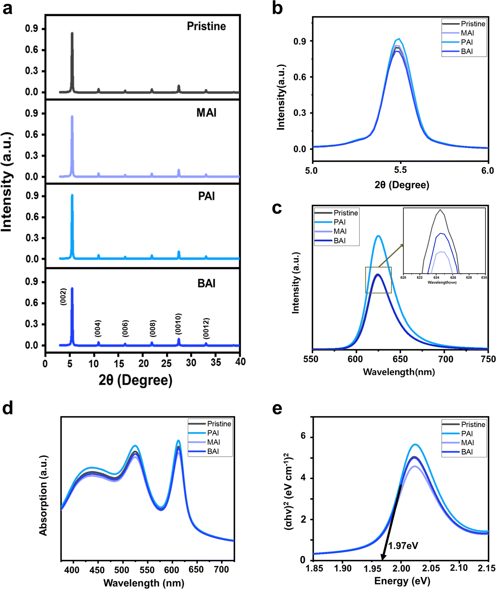 | ||
| Fig. 1 Thin film characteristics of (PEA)2SnI4 with and without alkylammonium additives (MAI, PAI, and BAI). (a) XRD patterns. (b) Magnification of (002) XRD diffraction peak. (c) Steady-state photoluminescence (PL) spectra with a magnified plot to show differences between similar peaks. (d) UV-vis absorption spectra. (e) Tauc plots. | ||
While the crystal structure remains unaffected by the small portion of alkyl ammonium additives, we observed a slightly higher XRD intensity in (PEA)2SnI4 films with PAI additives (Fig. 1b), indicative of enhanced crystallinity. This improved perovskite film quality with the PAI additive was further confirmed by steady state PL (Fig. 1c). In contrast to the PL spectra of the perovskite films with MAI and BAI, which showed similar intensity to that of the pristine perovskite film, the PL intensity of the perovskite film with PAI noticeably increased compared to the pristine film. This indicates that PAI, unlike other additives, effectively reduces non-radiative recombination within the film.
The improved film quality with PAI significantly enhances the performance of the FET devices. Fig. 2a illustrates the FET device structure, which features a (PEA)2SnI4 perovskite thin film as the channel layer, grown on a p+-Si/silicon dioxide (SiO2, 300 nm) substrate, with a bottom-gate-top-contact configuration. The transfer curves of the devices (at Vd = −40 V in the saturation regime, Fig. 2b–e) demonstrate a substantial performance enhancement in the device with PAI, compared to the pristine device. Specifically, the field-effect mobility (μFE) increased from 0.42 cm2 V−1 s−1 to 1.11 cm2 V−1 s−1, and the on–off current ratio (Ion/off) improved from 1.05 × 10⁵ to 3.76 × 10⁵. Additionally, the FET device with PAI exhibits a threshold voltage (Vth) closer to 0 V (from −6.17 V to −1.93 V) and a minimized subthreshold swing (SS) (reduced from 1.83 V dec−1 to 1.09 V dec−1). Conversely, the devices with MAI and BAI additives show decreased μFE and Ion/off, to 0.21 cm2 V−1 s−1 and 1.01 × 10⁴ for MAI, and to 0.18 cm2 V−1 s−1 and 3.88 × 10⁴ for BAI, respectively. Furthermore, their Vth and SS values are also degraded, to −14.3 V and 3.78 V dec−1 for MAI, and −18.4 V and 1.79 V dec−1 for BAI. This degradation is attributed to the induced perovskite lattice instability caused by these additives. All these data are based on average values from 30 devices, and these average values, including maximum values, are summarized in Table 1. The positive effects of additives on the 2D (PEA)2SnI4 perovskite structure will be further evaluated by density functional theory (DFT) calculations later.
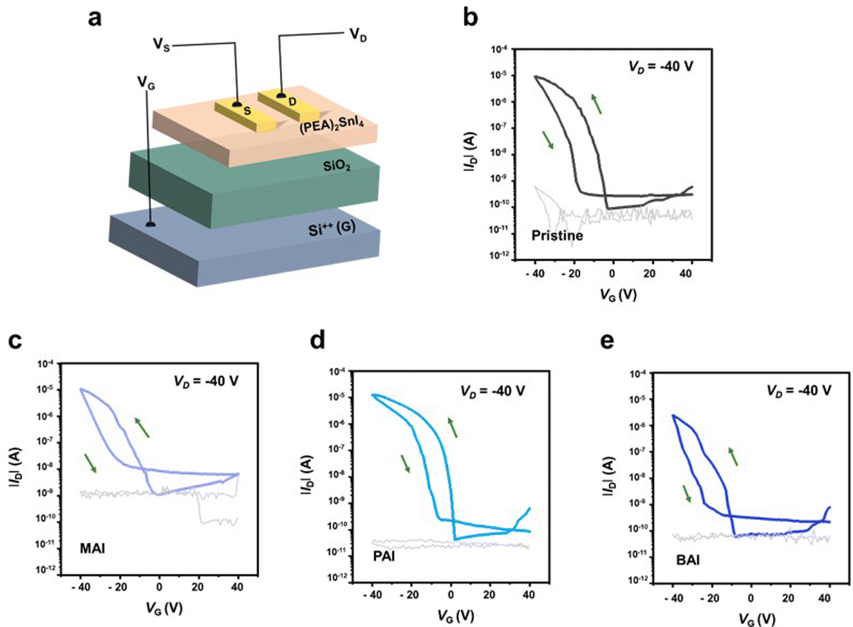 | ||
| Fig. 2 Transfer characteristics of bottom-gate-top-contact field-effect transistors (FETs) (VD = −40 V). Gray lines represent gate leakage current. (a) Schematic illustration of FET device. (b) Pristine (PEA)2SnI4. (c) (PEA)2SnI4 with MAI. (d) (PEA)2SnI4 with PAI. (e) (PEA)2SnI4 with BAI. | ||
| Pristine | MAI | PAI | BAI | PDAI2 | ||
|---|---|---|---|---|---|---|
| a Avg. values represent average ± standard deviation from forward scan curves of 30 devices. | ||||||
| μ FE (cm2 V−1 s−1) | Avg. | 0.42 ± 0.12 | 0.21 ± 0.12 | 1.11 ± 0.13 | 0.18 ± 0.11 | 2.41 ± 0.12 |
| Max. | 0.62 | 0.35 | 1.37 | 0.31 | 2.60 | |
| I on/Ioff | Avg. | 1.05 × 10⁵ | 1.01 × 10⁴ | 3.76 × 10⁵ | 3.88 × 10⁴ | 2.43 × 10⁶ |
| Max. | 2.34 × 10⁵ | 1.59 × 10⁴ | 8.13 × 10⁵ | 4.04 × 10⁴ | 5.08 × 10⁶ | |
| V th (V) | Avg. | −6.17 ± 1.06 | −14.3 ± 1.05 | −1.93 ± 1.09 | −18.4 ± 1.03 | −1.12 ± 0.89 |
| SS (V dec−1) | Avg. | 1.83 ± 0.14 | 3.78 ± 0.23 | 1.09 ± 0.11 | 1.79 ± 0.15 | 0.88 ± 0.12 |
| Min. | 1.68 | 2.54 | 0.97 | 1.58 | 0.75 | |
Inspired by the favorable impact of PAI on the (PEA)2SnI4 perovskite thin film, leading to improved FET performance, we introduced PDAI2, which contained an additional ammonium functional group, to the film (1 mol%). Similar to PAI, the introduction of PDAI2 resulted in minimal changes in the position of XRD peaks [(002): 5.5°, interlayer spacing 16.1 Å] (Fig. 3a and b) and no alterations in bandgap, as estimated by absorbance (Fig. 3d), Tauc plot (Fig. S1, ESI†), and PL spectra (Fig. 3e). However, with the addition of PDAI2, a slight increase in XRD peak intensity was observed compared to PAI (Fig. 3b), accompanied by a significant increase in PL intensity (Fig. 3e), suggesting more efficient suppression of non-radiative recombination compared to PAI. Scanning electron microscopy (SEM) analysis revealed a reduction in sharp grain boundaries seen in pristine films with the addition of PAI, which were further diminished with the addition of PDAI2 (Fig. 3f–h). To clearly show the morphological improvements in (PEA)2SnI4 induced by the additives, low-magnification SEM images (Fig. S2, ESI†) and non-contact mode AFM analyses (Fig. S3, ESI†) are provided. In particular, the AFM line profiles reveal variations in grain boundary depth: the pristine (PEA)2SnI4 film exhibits a depth of 39.47 nm, whereas the PAI and PDAI2 added films show reduced depths of 27.26 and 12.02 nm, respectively. This reduction indicates that PAI and PDAI2 effectively passivate the charged defects at the grain boundaries, thereby improving the overall film quality.17 As a result, the contact resistance at the device interface of the pristine film, estimated through the transmission line method, decreases with PAI and is further reduced with PDAI2 (Fig. 3c).
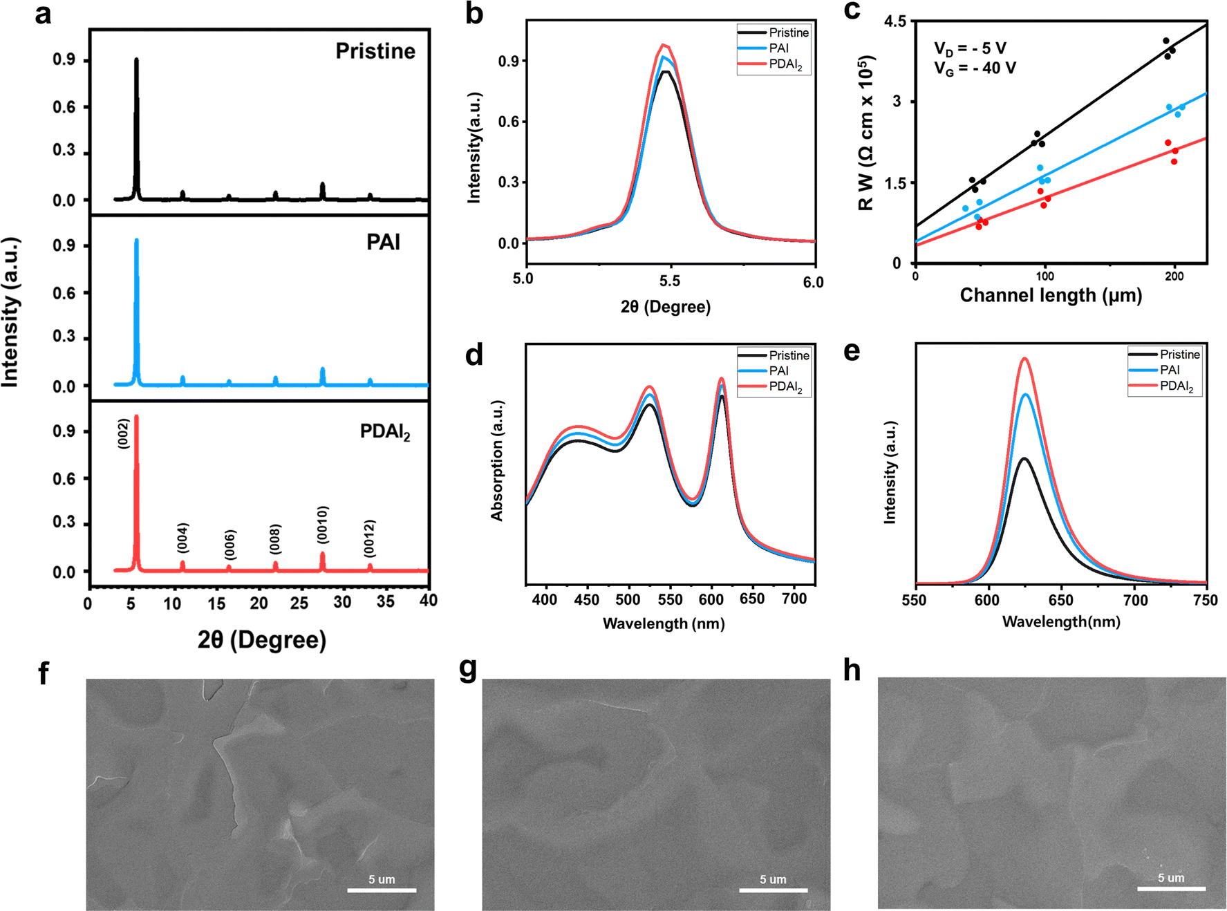 | ||
| Fig. 3 Thin film characteristics of (PEA)2SnI4 with and without alkylammonium additives (PAI and PDAI2). (a) XRD patterns. (b) Magnification of (002) XRD diffraction peak. (c) Transmission line method to estimate contact resistances of Sn halide perovskite FETs with and without additives (PAI and PDAI2). (d) UV-vis absorption spectra. (e) Steady-state PL spectra. SEM images of (f) pristine (PEA)2SnI4 film, (g) (PEA)2SnI4 film with PAI, and (h) (PEA)2SnI4 film with PDAI2 (scale bar: 5 μm). | ||
The improved film quality with additives such as PAI and PDAI2 is also confirmed by X-ray photoelectron spectroscopy (XPS) analysis. Fig. 4a–c show the core level spectra of Sn 3d5/2 and Sn 3d3/2, representing peaks at 486 and 494 eV, respectively. These peaks are further resolved into main peaks (485.5 eV and 494 eV) and two shoulder peaks at lower (484.5 eV and 493 eV) and higher binding energies (486.5 eV and 495 eV). The main peaks correspond to Sn2+ species, while the shoulder peaks at higher binding energies (486.5 eV and 495 eV) are associated with Sn4+ species in an oxidized state. These peaks are diminished with PAI and further reduced with PDAI2, indicating prevention of Sn oxidation from Sn2+ to Sn4+ by effective passivation. Additionally, the shoulder peaks at lower binding energies (484.5 eV and 493 eV) corresponding to undercoordinated Sn in an oxidized state (denoted as Snδ<2+)22 are also decreased with PAI and markedly reduced with PDAI2. The oxidation of Sn2+ to Sn4+ has been reported to generate Sn vacancies in the lattice, which act as hole traps and these vacancies contribute to charge trapping, negatively impacting hole charge transport.23 To further investigate the oxidation induced defect density within Sn perovskite bulk, we conducted space-charge limited current (SCLC) measurements using a hole-only device with the structure of [ITO/PEDOT:PSS/(PEA)2SnI4/PTAA/Ag] (Fig. S4, ESI†). The trap density (Ntrap) was calculated using the equation Ntrap = 2εεoVTFL(eL2)−1,24 where the trap-filled limited voltage (VTFL) was determined to be 0.778 V for pristine (PEA)2SnI4 films and decreased to 0.636 V and 0.581 V with the incorporation of PAI and PDAI2, respectively. Consequently, the trap density of pristine (PEA)2SnI4, initially 3.11 × 1016 cm−3 was reduced to 2.54 × 1016 cm−3 with PAI and further decreased to 2.32 × 1016 cm−3 with PDAI2. For reference, the energy band structures of perovskite films with and without additives (PAI and PDAI2) were investigated using ultra-violet photoelectron spectroscopy (UPS) (Fig. S5, ESI†). The work function (φ) was calculated using the equation: φ = hν − |Ecut-off − EF|, where Ecut-off and EF are the secondary electron cut-off energy and Fermi energy level, and the valence band maximum (VBM) is estimated from the onset energy.25 The conduction band minimum (CBM) was then estimated by incorporating the bandgap value obtained from the Tauc plot (Fig. S1, ESI†). The results indicate that the variations are minimal, demonstrating that the addition of a small portion of additives has only a marginal effect on the energy band structure.
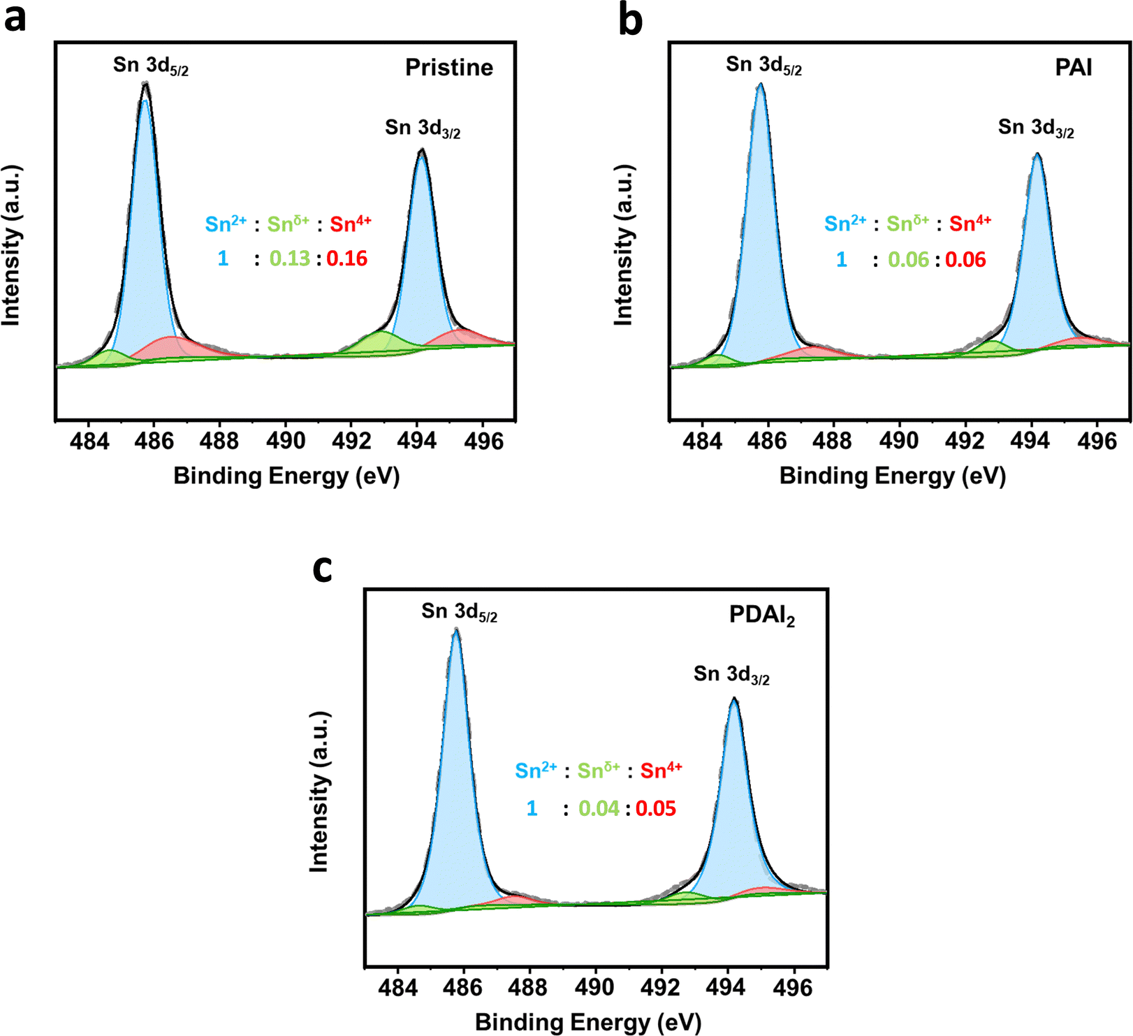 | ||
| Fig. 4 X-ray photoelectron spectroscopy (XPS) analysis of Sn 3d peaks in (PEA)2SnI4 films with and without alkylammonium additives (PAI and PDAI2). (a) Pristine (PEA)2SnI4 film. (b) (PEA)2SnI4 film with PAI. (c) (PEA)2SnI4 film with PDAI2. | ||
Consequently, the μFE and Ion/off of the FET device were further enhanced with PDAI2 compared to PAI, as demonstrated in the transfer curves (Fig. 5a–c). Specifically, μFE (in saturation regime) increased from 1.11 cm2 V−1 s−1 to 2.41 cm2 V−1 s−1, and Ion/off improved from 3.76 × 10⁵ to 2.43 × 10⁶. The corresponding output curves are presented in Fig. 5d–f. Additionally, compared to PAI, Vth further shifted with PDAI2 (from −1.93 V to −1.12 V), and SS values were further reduced (from 1.09 to 0.88). These data are based on average values from 30 devices, and the variations in μFE, Ion/off, Vth, and SS of the devices with and without additives (PAI and PDAI2) are summarized in Fig. 5g–j and Table 1. To accurately assess the mobility values of FET devices, we estimated the effective mobility (μeffective) by multiplying the claimed μFE by the reliability factor in the saturation regime (rsat).26 Detailed information regarding the mobility calculations and the obtained data is provided in Note 1 and Table S1 of the (ESI†). Additionally, the transfer characterization  , including fitting lines used for mobility calculations, is presented in Fig. S6 (ESI†).
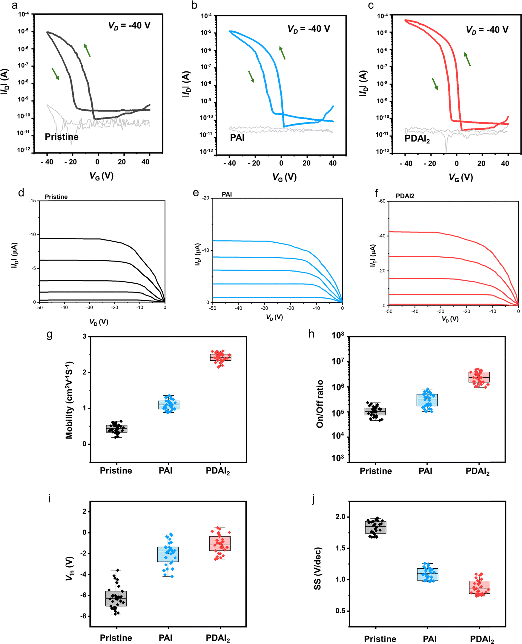 | ||
| Fig. 5 FET performance analysis. (a)–(c) Transfer characteristics of FETs (VD = −40 V). Gray lines represent gate leakage current: (a) pristine (PEA)2SnI4, (b) (PEA)2SnI4 with PAI, and (c) (PEA)2SnI4 with PDAI2. (d)–(f) Output characteristics of FETs (VG = 0, −10, −20, −30, −40 V): (d) pristine (PEA)2SnI4, (e) (PEA)2SnI4 with PAI, and (f) (PEA)2SnI4 with PDAI2. (g)–(j) FET performance metrics from 30 devices (box plot: the box represents the interquartile range, the line within the box indicates the median, and the whiskers show the maximum and minimum values): (g) field-effect mobility, (h) on/off current ratio, (i) threshold voltage (Vth), and (j) subthreshold swing (SS). | ||
The transfer curves of 30 FET devices with PDAI2-added perovskite are represented in Fig. S7 (ESI†). The maximum interface trap density (Nmax) within FET devices was also calculated from SS values using the equation27Nmax = [(SSloge)/(kT/q) − 1](Ci/q), where k is the Boltzmann constant, T is the absolute temperature, q is the elementary charge, and Ci is the capacitance of the insulator. Nmax is minimized in the FETs with PAI and PDAI2, being lowest with PDAI2 (Fig. S8, ESI†). For reference, the performance variation of FETs depending on the portion of additive (PAI and PDAI2) is investigated in Fig. S9 (ESI†), with 1 mol% showing the best performance.
To evaluate the operational stability of the FET devices, bias-stress stability tests were conducted by monitoring ID under constant gate and drain voltages (VG = −40 V and VD = −40 V). As shown in Fig. S10 (ESI†), the FET device with pristine perovskite retained less than 20% of its initial ID value after 2000 s, indicating noticeable carrier trapping within the device. However, the devices with PAI and PDAI2 exhibited much lower ID decay, retaining over 40% and 60% of their initial ID values, respectively, even after 2000 s. This suggests a reduction in trap states in the devices with these additives.28
To elucidate the advantageous effects of additive molecules on the perovskite structures, DFT calculations were conducted. In (PEA)2SnI4, PEA vacancies can be easily formed, and ammonium cations can effectively passivate these cation sites.29 Given that the defect passivation enhances device performance by mitigating non-radiative recombination centers within the perovskite,30 we calculated the formation energy (Eform) of various organic molecules that could fill a PEA vacancy, thereby improving the stability of (PEA)2SnI4 (Fig. 6a and b). The formation energy decreases as the length of carbon chain in the additive increases (methylammonium (MA+) → ethylammonium (EA+) → propylammonium (PA+)), which stabilizes the perovskite (Fig. 6a). However, the formation energy increases when the carbon chain length exceeds that of PA+, indicating an optimal chain length for perovskite stabilization. We also examined the effect of diammonium additives on the stability of the 2D (PEA)2SnI4 perovskite. Similarly, the formation energy decreased with increasing carbon chain length (methyldiammonium (MDA+) → ethane-1,2-diammonium (EDA+) → propane-1,3-diammonium (PDA+)), reaching its lowest at (PEA)1.5(PDA)0.5SnI4 (Eform = −2.65 eV), but increased when butane-1,4-diammonium (BDA+) was used, akin to the single ammonium group additives. Overall, diammonium additives exhibited lower formation energies than single ammonium group additives, regardless of carbon chain (Fig. 6a and b).
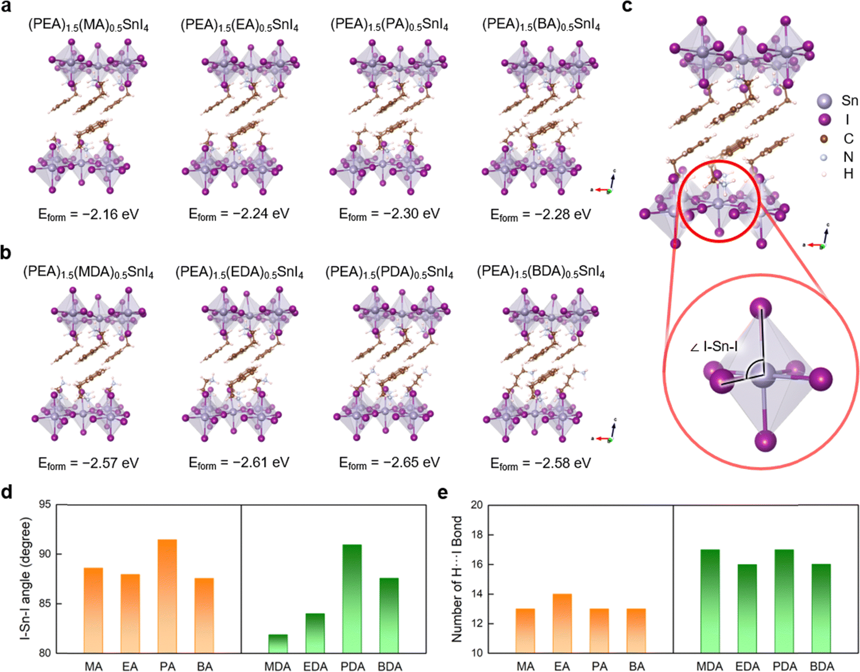 | ||
| Fig. 6 Density functional theory (DFT)-optimized 2D perovskite structures and formation energies (Eform) of organic cations for (a) (PEA)1.5(MA)0.5SnI4, (PEA)1.5(EA)0.5SnI4, (PEA)1.5(PA)0.5SnI4 and (PEA)1.5(BA)0.5SnI4, and (b) (PEA)1.5(MDA)0.5SnI4, (PEA)1.5(EDA)0.5SnI4, (PEA)1.5(PDA)0.5SnI4 and (PEA)1.5(BDA)0.5SnI4. (c) Illustration of equatorial I–Sn–axial I angle of (PEA)2SnI4 structure. (d) I–Sn–axial I angles and (e) the number of H⋯I bonds in the 2D perovskites with the addition of MA, EA, PA, BA, MDA, EDA, PDA, and BDA cations. | ||
To explore the origin of the formation energy differences influenced by carbon chain length, we initially examined the equatorial I–Sn–axial I angle (Fig. 6c). Greater deviation from the ideal octahedral structure (90°) increases distortion and instability in perovskite materials.31 The equatorial I–Sn–axial I angle varied with the number of carbon atoms, with angles in propylammonium (PA+) and propyldiammonium (PDA+) approaching 90° more closely than in other cases, thus promoting an ideal octahedron formation (Fig. 6d). This suggests that steric hindrance, dependent on the number of carbon atoms, affects the stability of the inorganic framework.32,33
We also evaluated the impact of increased ammonium groups by quantifying the number of H⋯I bonds shorter than 3.0 Å, which serve as indicators of effective hydrogen bonding and contribute to the overall structural stability of organic–inorganic halide perovskites. Our results showed a higher number of hydrogen bonds in diammonium additives (MDA+, EDA+, PDA+, and BDA+) compared to monoammonium additives (MA+, EA+, PA+, and BA+) (Fig. 6e). The increased hydrogen bonding due to diammonium groups further stabilizes the 2D perovskite structures, enhancing their structural robustness (e.g., raising their melting temperature), as previously reported.34 Additionally, the average Sn–axial I bond length increased with diammonium additives (Fig. S11, ESI†), which can be attributed to the H⋯I hydrogen bonding interaction. Therefore, the incorporation of organic molecules with diammonium groups results in a higher number of hydrogen bonds, providing greater stabilization to the system compared to the additives with a single ammonium group.
Considering that strong van der Waals interactions between organic ligands stabilize the 2D perovskite structure, longer chain lengths seem more appropriate as additives.35 However, structural mismatches, such as octahedral tilting and size mismatches between the cavity size of PEA vacancies and the length of addictive molecules, could destabilize the perovskite structure. Therefore, an optimal carbon chain length likely exists. Consequently, the PDA additive enhances device efficiency and stability by effectively passivating the PEA vacancies.
4. Conclusion
We investigate the impact of various alkyl ammonium-iodide additives on the structural and electronic properties of (PEA)2SnI4 perovskite films. XRD analysis reveals that a small portion (1 mol%) of these additives does not alter the crystal lattice structure, maintaining consistent interlayer spacing and bandgap values across all samples. However, films with PAI and PDAI2 additives exhibit enhanced crystallinity, reduced non-radiative recombination, and diminished Sn oxidation. DFT calculations demonstrate that the formation energy is minimized with PAI and PDAI2 due to the equatorial I–Sn–axial I angle within the perovskite octahedron approaching 90°, suggesting that steric hindrance, dependent on the number of carbon atoms, affects the stability of the inorganic framework. Furthermore, PDAI2, with an additional ammonium group, increases effective H⋯I hydrogen bonding between ammonium and halide ions, further stabilizing the 2D perovskite structures and enhancing their structural robustness. The improved film quality with PDAI2 significantly enhances FET device performance, as evidenced by increased μFE (maximum 2.6 cm2 V−1 s−1) and Ion/off (>106), more favorable Vth (approaching 0), and reduced SS values.Data availability
The data supporting this article have been included as part of the ESI.†Conflicts of interest
There are no conflicts to declare.Acknowledgements
This research was financially supported by the National Research Foundation of Korea (NRF) (RS-2024-00350701). This research was also supported by Korea Basic Science Institute (National Research Facilities and Equipment Center) grant funded by the Ministry of Education (RS-2024-00436346).References
- X.-K. Liu, W. Xu, S. Bai, Y. Jin, J. Wang, R. H. Friend and F. Gao, Nat. Mater., 2021, 20, 10–21, DOI:10.1038/s41563-020-0784-7
.
- A. G. Ricciardulli, S. Yang, J. H. Smet and M. Saliba, Nat. Mater., 2021, 20, 1325–1336, DOI:10.1038/s41563-021-01029-9
- L. M. Herz, ACS Energy Lett., 2017, 2, 1539–1548, DOI:10.1021/acsenergylett.7b00276
- X. Liu, D. Yu, X. Song and H. Zeng, Small, 2018, 14, 1801460, DOI:10.1002/smll.201801460
- J. G. Labram, D. H. Fabini, E. E. Perry, A. J. Lehner, H. Wang, A. M. Glaudell, G. Wu, H. Evans, D. Buck, R. Cotta, L. Echegoyen, F. Wudl, R. Seshadri and M. L. Chabinyc, J. Phys. Chem. Lett., 2015, 6, 3565–3571, DOI:10.1021/acs.jpclett.5b01669
- D. Ghosh, E. Welch, A. J. Neukirch, A. Zakhidov and S. Tretiak, J. Phys. Chem. Lett., 2020, 11, 3271–3286, DOI:10.1021/acs.jpclett.0c00018
- J. Cho, J. T. DuBose, A. N. T. Le and P. V. Kamat, ACS Mater. Lett., 2020, 2, 565–570, DOI:10.1021/acsmaterialslett.0c00124
- Y. Gao, Z. Wei, P. Yoo, E. Shi, M. Zeller, C. Zhu, P. Liao and L. Dou, J. Am. Chem. Soc., 2019, 141, 15577–15585, DOI:10.1021/jacs.9b06276
- Y. Chen, Y. Sun, J. Peng, J. Tang, K. Zheng and Z. Liang, Adv. Mater., 2018, 30, 1703487, DOI:10.1002/adma.201703487
- W. Yang, L. Dou, H. Zhu and Y.-Y. Noh, Small Struct., 2024, 230393, DOI:10.1002/sstr.202300393
- H. Zhu, A. Liu, H. Kim, J. Hong, J.-Y. Go and Y.-Y. Noh, Chem. Mater., 2021, 33, 1174–1181, DOI:10.1021/acs.chemmater.0c03822
- T. Matsushima, S. Hwang, A. S. D. Sandanayaka, C. Qin, S. Terakawa, T. Fujihara, M. Yahiro and C. Adachi, Adv. Mater., 2016, 28, 10275–10281, DOI:10.1002/adma.201603126
- I. Chao, Y.-T. Yang, M.-H. Yu, C.-H. Chen, C.-H. Liao, B.-H. Lin, I. Ni, W. Y. Ho-Baillie and C.-C. Chuenh, Small, 2023, 19, 2207734, DOI:10.1002/smll.202207734
- X. Qiu, J. Xia, Y. Liu, P.-A. Chen, L. Huang, H. Wei, J. Ding, Z. Gong, X. Zeng, C. Peng, C. Chen, X. Wang, L. Jiang, L. Liao and Y. Hu, Adv. Mater., 2023, 35, 2305648, DOI:10.1002/adma.202305648
- S. Wang, K. Bidinakis, C. Haese, F. H. Hasenburg, O. Yildiz, Z. Ling, S. Frisch, M. Kivala, R. Graf, P. W. M. Blom, S. A. L. Weber, W. Pisula and T. Marszalek, Small, 2023, 19, 1613–6810, DOI:10.1002/smll.202207426
- Y. Yang, J. Song, Y. L. Zhao, L. Zhu, X. Q. Gu, Y. Q. Gu, M. Che and Y. H. Qiang, J. Alloys Compd., 2016, 684, 84–90, DOI:10.1016/j.jallcom.2016.05.154
- B. Ma, J. Chen, M. Wang, X. Xu, J. Qian, Y. Lu, W. Zhang, P. Xia, M. Qin, W. Zhu, L. Zhang, S. Chen, X. Lu and W. Huang, J. Phys. Chem. C, 2020, 124, 16289–16299, DOI:10.1021/acs.jpcc.0c03401
- S. Liu, X. Guan, W. Xiao, R. Chen, J. Zhou, F. Ren, J. Wang, W. Chen, S. Li, L. Qiu, Y. Zhao, Z. Liu and W. Chen, Adv. Funct. Mater., 2022, 32, 2205009, DOI:10.1002/adfm.202205009
- E. Jokar, C.-H. Chien, A. Fathi, M. Rameez, Y.-H. Chang and E. W.-G. Diau, Energy Environ. Sci., 2018, 11, 2353–2362, 10.1039/C8EE00956B
- C. Liu, Y. Yang, H. Chen, J. Xu, A. Liu, A. S. R. Bati, H. Zhu, L. Grater, S. S. Hadke, C. Huang, V. K. Sangwan, T. Cai, D. Shin, L. X. Chen, M. C. Hersam, C. A. Mirkin, B. Chen, M. G. Kanatzidis and E. H. Sargent, Science, 2023, 382, 810–815, DOI:10.1126/science.adk1633
- L. Zhang, Q. Kang, H. Shi, J. Hong, Y. Song, D. Chi, S. Huang and G. He, Sol. RRL, 2021, 5, 2100299, DOI:10.1002/solr.202100299
- L. E. Mundt, J. Tong, A. F. Palmstrom, S. P. Dunfield, K. Zhu, J. J. Berry, L. T. Schelhas and E. L. Ratcliff, ACS Energy Lett., 2020, 5, 3344–3351, DOI:10.1021/acsenergylett.0c01445
- Y. J. Heo, H. J. Jang, J.-H. Lee, S. B. Jo, S. Kim, D. H. Ho, S. J. Kwon, K. Kim, I. Jeon, J.-M. Myoung, J. Y. Lee, J.-W. Lee and J. H. Cho, Adv. Funct. Mater., 2021, 31, 2106974, DOI:10.1002/adfm.202106974
- J. Yong, Y. K. Lee, H. Park, S. Muthu, J. Shin, D. R. Whang, B.-G. Kim, D. W. Chang and H. J. Park, Adv. Funct. Mater., 2024, 34, 2312505, DOI:10.1002/adfm.202312505
- J. Heo, J. A. Prayogo, S. W. Lee, H. Park, S. Muthu, J. Hong, H. Kim, Y.-H. Kim, D. R. Whang, D. W. Chang and H. J. Park, Small, 2024, 20, 2404784, DOI:10.1002/smll.202404784
- H. H. Choi, K. Cho, C. D. Frisbie, H. Sirringhaus and V. Podzorov, Nat. Mater., 2018, 17, 2–7, DOI:10.1038/nmat5035
- A. Rolland, J. Richard, J. P. Kleider and D. Mencaraglia, J. Electrochem. Soc., 1993, 140, 3679, DOI:10.1149/1.2221149
- W. H. Lee, H. H. Choi, D. H. Kim and K. Cho, Adv. Mater., 2014, 26, 1660–1680, DOI:10.1002/adma.201304665
- S. Kahmann, D. Meggiolaro, L. Gregori, E. K. Tekelenburg, M. Pitaro, S. D. Stranks, F. D. Angelis and M. A. Loi, ACS Energy Lett., 2022, 7, 4232–4241, DOI:10.1021/acsenergylett.2c02123
- R. Lin, J. Xu, M. Wie, Y. Wang, Z. Qin, Z. Liu, J. Wu, K. Xiao, B. Chen, S. M. Park, G. Chen, H. R. Atapattu, K. R. Graham, J. Xu, J. Zhu, L. Li, C. Zhang, E. H. Sargent and H. Tan, Nature, 2022, 603, 73–78, DOI:10.1038/s41586-021-04372-8
- L. Kong, Y. Sun, B. Zhaon, K. Ji, J. Feng, J. Dong, Y. Wang, Z. Liu, S. Maqbool, Y. Li, Y. Yang, L. Dai, W. Lee, C. Cho, S. D. Stranks, R. H. Friend, N. Wang, N. C. Greenham and X. Yang, Nature, 2024, 631, 73–79, DOI:10.1038/s41586-024-07531-9
- W. Paritmongkol, N. S. Dahod, A. Stollmann, N. Mao, C. Settens, S.-L. Zheng and W. A. Tisdale, Chem. Mater., 2019, 31, 5592–5607, DOI:10.1021/acs.chemmater.9b01318
- T. Hossain, H. R. Atapattu, H. Pruett, M. T. Rahman, K. R. Pedersen, A. J. Huckaba, S. R. Parkin and R. Graham, Chem. Mater., 2024, 36, 11004–11014, DOI:10.1021/acs.chemmater.4c01251
- J. Son, S. Ma, Y.-K. Jung, J. Tan, G. Jang, H. Lee, C. U. Lee, J. Lee, S. Moon, W. Jeong, A. Walsh and J. Moon, Nat. Commun., 2023, 14, 3124, DOI:10.1038/s41467-023-38927-2
- J. Xing, Y. Zhao, M. Askerka, L. N. Quan, X. Gong, W. Zhao, J. Zhao, H. Tan, G. Long, L. Gao, Z. Yang, O. Voznyy, J. Tang, Z.-H. Lu, Q. Xiong and E. H. Sargent, Nat. Commun., 2018, 9, 3541, DOI:10.1038/s41467-018-05909-8
Footnotes |
| † Electronic supplementary information (ESI) available. See DOI: https://doi.org/10.1039/d4tc05307a |
| ‡ These authors contribute equally to this work |
| This journal is © The Royal Society of Chemistry 2025 |