
Thermal management broadband-emitting device based on VO2 applied in the mid-infrared band
Ying
Zheng
a,
Zhiyou
Wang
*b,
Qianju
Song
 a,
Zao
Yi
*ac,
Shubo
Cheng
d and
Yougen
Yi
e
a,
Zao
Yi
*ac,
Shubo
Cheng
d and
Yougen
Yi
e
aSchool of Mathematics and Science, Joint Laboratory for Extreme Conditions Matter Properties, The State Key Laboratory of Environment-Friendly Energy Materials, Tianfu Institute of Research and Innovation, Southwest University of Science and Technology, Mianyang 621010, China. E-mail: yizaomy@swust.edu.cn
bSchool of Electronic Information and Electric Engineering, Changsha University, Changsha 410022, China. E-mail: zywang@ccsu.edu.cn
cSchool of Chemistry and Chemical Engineering, Jishou University, Jishou 416000, China
dSchool of Physics and Optoelectronic Engineering, Yangtze University, Jingzhou, Hubei 434023, China
eCollege of Physics, Central South University, Changsha 410083, China
First published on 14th January 2025
Abstract
Mid-infrared thermal radiation has attracted attention due to its wide range of applications. Compared to the static process of thermal emission, if thermal radiation can be dynamically controlled, it would be more suitable for practical applications. Herein, we designed a controllable thermal emitter based on phase change materials. When the temperature changes from low to high, VO2 transitions from a dielectric state to a metallic state, and its imaginary part of the dielectric constant significantly increases, leading to differences in emission characteristics. At low temperatures, the device is in a low dielectric state and resonates weakly with incident light. The main emission comes from the bottom of the grating structure, with an emissivity of 0.21. At high temperatures, the structure is in a high dielectric state, and multiple resonance modes are excited within the structure, such as cavity resonance and surface plasmon resonance, which increases the emissivity to 0.95 and achieves effective heat dissipation. Given its superior thermal management capabilities and stability, this design holds promise for applications in thermal imaging, infrared communication, and energy-efficient devices.
1. Introduction
Thermal radiation refers to an object radiating electromagnetic waves outward due to its own temperature, often occurring in the infrared band. At the beginning of the 20th century, Planck summarized the blackbody radiation law based on his predecessor's work,1 laying an important theoretical foundation for thermal radiation. The research on thermal radiation is of great significance, as functions such as stealth,2,3 thermal management,4–7 and infrared detection8 can be achieved by manipulating radiation energy in different bands. In the mid-20th century, Richard Feynman noted the significance of ‘nanoscale’ for future technological development.9 Subsequently, over a period of several decades, micro and nano processing techniques flourished, gradually shifting the combination of thermal radiation and micro/nanostructures from theory to practice.10,11 By designing micro and nanostructures with different materials, sizes, and shapes, it is possible to control thermal radiation.Based on Stefan Boltzmann's law, the energy intensity radiating into the environment is related to temperature and emissivity.12,13 Due to the usual lack of consideration for temperature changes caused by a large amount of energy input, the control of thermal radiation mainly depends on modifying the emissivity of an object. The emissivity spectra regulation of thermal radiation can be mainly divided into two categories: static regulation and dynamic regulation.14–16 Static regulation refers to the situation where the optical characteristics of a device no longer change after its design and processing are completed. In contrast, dynamic adjustment is more flexible and can better meet a wide range of application needs. Dynamic regulation includes optical regulation,17 electrical regulation,18 thermal regulation,19 chemical regulation,20 mechanical regulation,21 and magnetic regulation.22 Among them, thermal regulation utilizes the phenomenon of material physical properties changing with temperature, resulting in devices exhibiting different optical properties at different temperatures.
VO2 is a thermochromic material that exhibits a unique insulator-to-metal transition at approximately 68 °C, allowing it to dynamically adjust its emissivity based on temperature changes.23,24 This transition from a dielectric to a metallic state is attributed to the reorganization of vanadium atoms within VO2 at higher temperatures, leading to changes in electronic structure.25,26 By utilizing this feature, many dynamic emissivity adjustments have emerged.
Gu et al. proposed a structure based on VO2/HfO2/Al.27 Working as an infrared reflector at low temperatures and as an infrared emitter at high temperatures, the emissivity adjustability in a 2.5–25 μm range reached 0.51, demonstrating excellent infrared radiation regulation function. Liu et al. reported an infrared adaptive broadband transmitter that achieved emissivity modulation from 0.21 to 0.75 during VO2's phase transition,28 and this device can be used for thermal management and infrared camouflage applications in spacecraft. Ma et al. proposed a metal–insulator–metal (MIM) structure with an inserted VO2 interlayer.29 Based on its magnetic pole, surface plasma, and phase transition characteristics with VO2, broadband emission tunable characteristics were achieved in an atmospheric window. Thus, the micro–nano structure based on the phase change material (PCM) VO2 is widely used in infrared emission modulation.
At present, the problems of high or low temperatures faced by buildings, vehicles, and outdoor equipment need to be effectively addressed. We have designed an easy-to-manufacture three-layer structure based on VO2, and optimized the emission modulation to 0.74 in the mid-infrared band (1.5–5 μm) by changing the structural parameters. The device exhibits excellent thermal management performance and is suitable for engineering and construction applications.
2. Structural design and material selection
We simulated and calculated the structure shown in Fig. 1. The bottom layer is made of Au (height H4 = 50 nm), which exhibits high reflectivity in the infrared band and is used as a reflective layer. The middle layer is Al2O3 (height H3 = 250 nm), which exhibits high transparency in the infrared region and serves as a dielectric spatial layer. The top is a VO2 grating with a height of 350 nm that serves as the absorption layer. In addition, H2 = 300 nm, L1 = 350 nm, L2 = 50 nm, and L3 = 100 nm. The dielectric constants of Au and Al2O3 are derived from Palik.30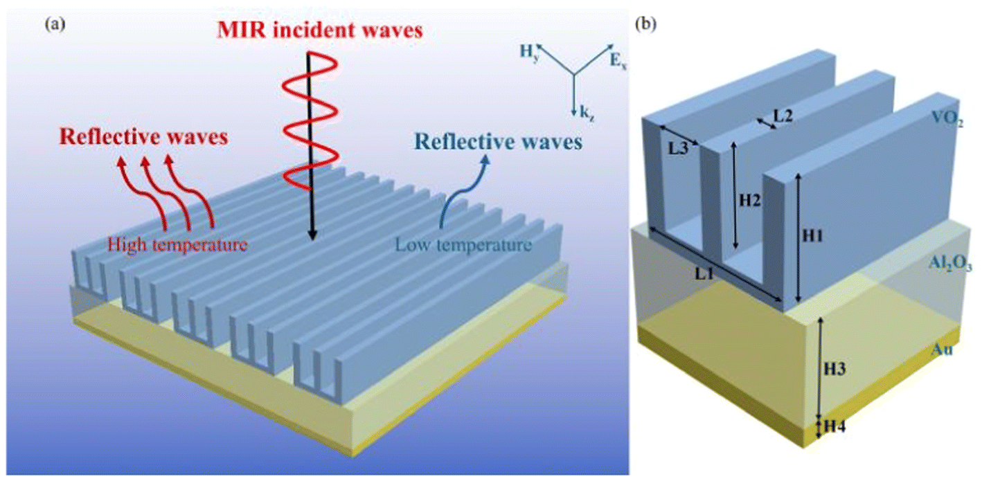 | ||
| Fig. 1 (a) Structural diagram of solar absorber; (b) a schematic diagram of the structure of one period. | ||
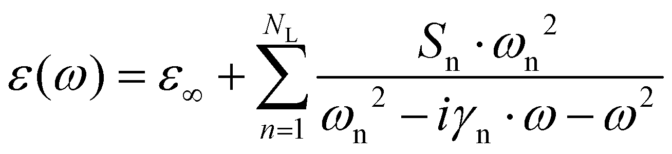
Fig. 2 shows the complex dielectric constant of VO2 in different states. In Fig. 2(a), at low temperatures, VO2 exhibits uniaxial anisotropic dielectric properties. It assumes different responses depending on whether the incident light is perpendicular or parallel to the optical axis. For normal incidence, only the first scenario applies. Both of these situations can be represented by the Lorentz model:31–33
 | (1) |
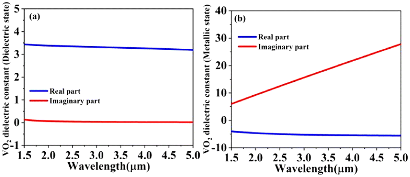 | ||
| Fig. 2 (a and b) The dielectric constants of VO2 at low and high temperatures, respectively. | ||
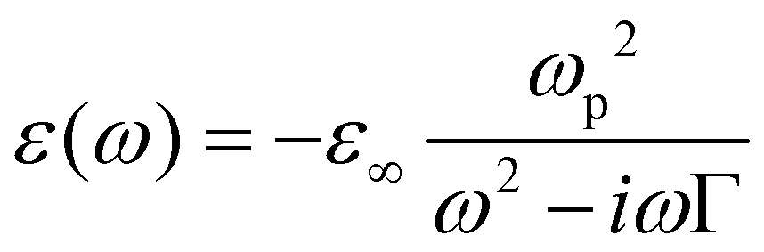
As the temperature increases and exceeds the phase transition temperature, VO2 exhibits a metallic state (isotropic metal), as shown in Fig. 2(b), and the complex dielectric constant is expressed as eqn (2):34,35
 | (2) |
3. Simulation results and discussion
3.1 Simulation results
Fig. 3 shows the infrared emission characteristics of the structure. Tunable infrared emission in the 1.5–5 μm band serves to facilitate temperature control and thermal management of devices, safeguarding them against overheating or undercooling effects. By Kirchhoff's law, the emissivity equals the absorptivity at thermal equilibrium. Therefore, the emissivity in Fig. 3 is calculated from eqn (3):36,37| ε(λ) = 1 − R(λ) − T(λ) | (3) |
 | (4) |
 | (5) |
 | ||
| Fig. 3 The absorption and reflection efficiency of the structure when VO2 is in different states. | ||
According to Fig. 3, VO2 exhibits a dielectric state with weak resonance with incident light at low temperature, resulting in an emissivity of less than 0.35 across the entire wavelength range, and an emissivity of less than 0.2 in the 3.36–5 μm range. After calculation, the average infrared emissivity at low temperature is 0.21. At high temperature, VO2 exhibits a metallic state with strong resonance modes within its structure, resulting in an enhanced emissivity across the entire band. The emissivity in the 1.5–4.6 μm range is greater than 0.9, and the overall average emissivity increases to 0.95. Because the emission tunability of this structure in the range of 1.5–5 μm reaches 0.74, it is suitable for applications in thermal management.
Fig. 4 shows the influence of different polarized waves and incident angles on structure. Comparing Fig. 4(a) and (b), there is a significant difference in the emission spectra of the structure depending upon whether under TE (transverse electricity) or TM (transverse magnetic) waves.40,41 In Fig. 4(a), under TE waves, the emissivity of the structure at different incident angles is generally greater than 0.9 and can even reach 0.99. As shown in Fig. 4(b), under TM waves, the emissivity significantly decreases, with a maximum of only 0.71. The difference in emission spectra between TE and TM waves arises from the orientation-dependent interaction of light with the grating structure, where there is more accurate alignment of TE polarization with the grating lines, which enhances resonance effects. However, the emissivity is less affected by the incident angle.
 | ||
| Fig. 4 (a and b) Under TE and TM waves, the absorption spectrum varies with the incident angle. | ||
As shown in Fig. 4(a), as the incident angle increases from 0° to 40°, the emission spectrum remains nearly unchanged before gradually decreasing with further increases in the incident angle. Until the incident angle exceeds 40°, the emissivity begins to significantly decrease. However, it is still greater than 70%. The trend shown in Fig. 4(b) is similar to that shown in Fig. 4(a), where the change in emissivity can be ignored between incident angles of 0–50°, until at approximately 55°, the emissivity begins to significantly decrease. Despite limitations due to polarization effects, the structure's angle insensitivity offers broad potential applications.
3.2 Physical mechanisms governing thermal emission
To analyze the thermal emission mechanism, we performed calculations of the electric field distribution. As shown in Fig. 5(a), at low temperatures, some electric fields are distributed outside the grating and in the Al2O3, originating from surface plasmon resonance (SPR) excitation.42,43 The weak electric field inside the grating originates from the excitation of cavity resonance. In addition, the strong electric field is confined to the angular space between VO2 and Al2O3, and mainly originated from local surface plasmon resonance (LSPR).44,45 As the temperature increases, in Fig. 5(b), the electric field localization between VO2 and Al2O3 increases, and a strong localized electric field is distributed at the top of the metallic VO2 grating. The electric field distribution inside the grating also extends from the lower half to the entire cavity, and the intensity increases, indicating that the cavity resonance in metallic vanadium dioxide is stronger.46 | ||
| Fig. 5 (a and b) An electric field distribution diagram of the XOZ plane at low and high temperatures at 2.18 μm. | ||
In addition, an increase in the highest electric field strength was observed from low temperature to high temperature. Thus, at low temperatures, weaker electric fields are observed because the dielectric VO2 does not support strong resonant modes. As temperature increases, enhanced electric field localization occurs due to the metallic VO2's ability to sustain stronger plasmonic resonances, resulting in a significant increase in emissivity.
Combining power density with electric field distribution enhances understanding of the physical mechanisms involved. The power density can be obtained from eqn (6):47,48
| Q = 0.5ωε0[ε′′(x)|E(x)|2 + ε′′(z)|E(z)|2] | (6) |
 | ||
| Fig. 6 (a and b) The power dissipation density of the XOZ plane at high and low temperatures at 2.18 μm. | ||
3.3 The influence of structural parameters
The optimal parameters were determined through finite-difference time-domain (FDTD) layer-domain scanning.49,50 In Fig. 7, the scanning process of gratings with different lengths is shown. From Fig. 1, L1 is the overall width of the grating structure. As Fig. 7(a) shows, with the increase in L1 from 310 nm to 350 nm, the emissivity shows an increasing trend, especially in the 1.5–1.8 μm and 3.7–5 μm bands where the emissivity significantly increases, resulting in bandwidth widening.51,52 However, as L1 continues to increase, the emissivity at 2.5–3.5 μm begins to decrease. Therefore, L1 = 350 nm is an ideal parameter. Fig. 7(b) shows a similar but opposite trend to Fig. 7(a). As L2 increases from 10 nm to 90 nm, the emissivity of the 1.5–2 μm and 4–5 μm bands gradually decreases, leading to a reduction in absorption bandwidth. However, the absorption gradually increases at 2.5–3.5 μm and remains almost unchanged until L2 = 50 nm. Therefore, a wider bandwidth and higher emissivity were simultaneously obtained only when L2 = 50 nm.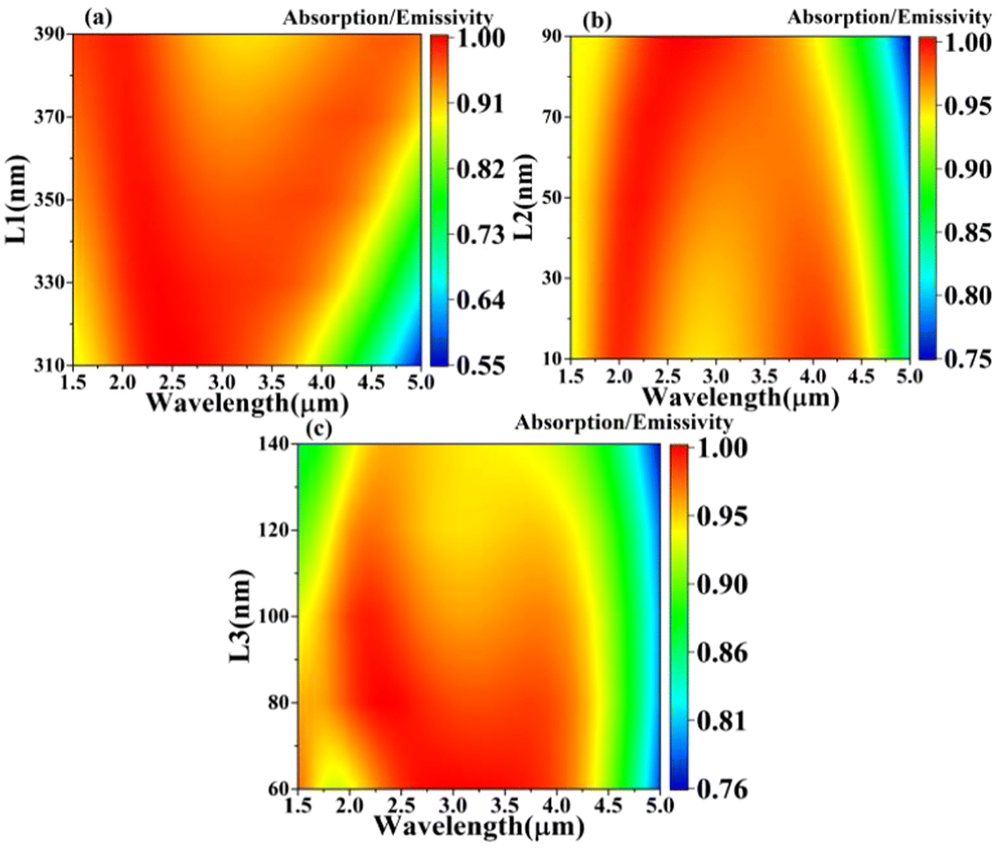 | ||
| Fig. 7 (a–c) The power dissipation density of the XOZ plane at high and low temperatures at 2.18 μm. | ||
L3 is the width of the grating groove, and when it increases to 100 nm, the spectral changes are weak, except for an increase in absorption at 1.7–2 μm. However, as L3 continues to increase, it is observed that the emissivity of nearly the entire band decreases, while the bandwidth shortens. Therefore, L3 = 100 nm is an ideal parameter. We can finally determine that the optimal parameters of h1 and h2 in the solar absorber model we designed are 700 nm and 100 nm, respectively.
Several film layer thicknesses were scanned, and Fig. 8(a) shows the scanning process for grating thickness. As H1 increases from 250 nm to 350 nm, the emissivity of multiple bands shows an increasing trend, but the significant increase no longer exists after 350 nm, and the emissivity of the 4–5 μm band begins to decrease. Therefore, H1 = 350 nm is an ideal parameter. Fig. 8(b) shows a trend similar to that to Fig. 8(a), but with a faster degree of change. When H2 = 280 nm, the average emissivity is 0.62. As the thickness increases to 300 nm, the emissivity also increases to 0.95. However, as the thickness incrementally increases, the emissivity exhibits a downward trend, culminating at a value of 0.88. This indicates that 300 nm is an ideal parameter for H2. As shown in Fig. 8(c), as H3 increases to 250 nm, the absorption efficiency in the long wavelength significantly increases, but it decreases as the thickness continues to increase.53,54 Numerically, the emissivity of H3 at 150 nm, 250 nm, and 350 nm is 0.64, 0.95, and 0.90, respectively. Therefore, H3 = 250 nm is an ideal parameter. Through this optimization process, we achieved an ideal balance between bandwidth and emissivity, demonstrating the structure's potential for applications in efficient thermal management.55–57
 | ||
| Fig. 8 (a–c) The power dissipation density of the XOZ plane at high and low temperatures at 2.18 μm. | ||
4. Conclusion
We designed a multi-layer device using the PCM VO2 that consists of a top grating layer, an Al2O3 dissipative film, and an Au reflective film, achieving thermal management in the 1.5–5 μm wavelength range. At low temperatures, VO2 is in a dielectric state, and the emissivity is 0.21; at high temperatures, VO2 is in a metallic state, and the emissivity is 0.95. The emission tunability reached 0.74, and this achievement provides an efficient and stable thermal management solution suitable for applications in building energy conservation, smart windows, aerospace thermal control, and more.Furthermore, this study delves into the physical mechanisms underlying the transformation from the dielectric state to the metallic state in VO2, elucidating the excitation of various resonance modes such as surface plasmon resonance (SPR) and cavity resonance under different temperature conditions. These insights deepen our understanding of VO2 material properties and their applications in micro/nanostructures, providing valuable theoretical foundations and technical guidance for subsequent research.
Data availability
The data are available from the corresponding author on reasonable request.Conflicts of interest
The authors declare that they have no known competing financial interests or personal relationships that could have appeared to influence the work reported in this paper.Acknowledgements
The authors are grateful for the support by the National Natural Science Foundation of China (No. 51606158, 11604311, 12074151); the Guangxi Science and Technology Base and Talent Special Project (No. AD21075009); the Sichuan Science and Technology Program (No. 2021JDRC0022); the Natural Science Foundation of Fujian Province (2022J011102, 2022H0048); the Open Fund of the Key Laboratory for Metallurgical Equipment and Control Technology of Ministry of Education in Wuhan University of Science and Technology, China (No. MECOF2022B01; MECOF2023B04); and the Guangxi Key Laboratory of Precision Navigation Technology and Application, Guilin University of Electronic Technology (No. DH202321).References
- M. Planck, The theory of heat radiation, Blakiston, 1914 Search PubMed.
- B. F. Guo, Y. J. Wang, C. F. Cao, Z. H. Qu, J. Song, S. N. Li, J. F. Gao, P. Song, G. D. Zhang and Y. Q. Shi, Adv. Sci., 2024, 11, 2309392 CrossRef CAS PubMed.
- Y. F. Xiao, C. Ma, T. Y. Sun, Q. J. Song, L. Bian, Z. Yi, Z. Q. Hao, C. J. Tang, P. H. Wu and Q. D. Zeng, J. Mater. Chem. A, 2024, 12, 29145 RSC.
- A. K. Thakur, R. Sathyamurthy, R. Velraj, R. Saidur, A. K. Pandey, Z. Ma, P. Singh, S. K. Hazra, S. W. Sharshir and R. Prabakaran, Appl. Therm. Eng., 2023, 226, 120303 CrossRef.
- S. L. Jiang, F. F. Chen, Y. Zhao, S. F. Gao and Y. Y. Wang, et al. , Opto-Electron. Adv., 2023, 6, 220085 CAS.
- Y. Liu, X. Ma, K. Chao, F. Sun, Z. Chen, J. Shan, H. Chen, G. Zhao and S. Chen, Opto-Electron. Sci., 2024, 3, 230027 CAS.
- S. R. Liang, S. B. Cheng, H. F. Zhang, W. X. Yang, Z. Yi, Q. D. Zeng, B. Tang, P. H. Wu, S. Ahmad and T. Y. Sun, Ceram. Int., 2024, 50, 23611–23620 CrossRef CAS.
- J. Ma, P. H. Wu, W. X. Li, S. R. Liang, Q. Y. Shangguan, S. B. Cheng, Y. H. Tian, J. Q. Fu and L. B. Zhang, Diamond Relat. Mater., 2023, 136, 109960 CrossRef CAS.
- R. Feynman, in Feynman and computation, CRC Press, 2018, pp. 63–76 Search PubMed.
- J. Zhu, J. Deng, H. Xiong, B. X. Wang and H. Q. Zhang, ACS Appl. Electron. Mater., 2024, 6(12), 9184–9193 CrossRef CAS.
- H. Xiong, Q. Yang, Y. Z. Huang, J. H. Deng, B. X. Wang and H. Q. Zhang, ACS Appl. Mater. Interfaces, 2024, 16(44), 60189–60196 CrossRef CAS PubMed.
- Y. Zhang, Y. Chen, T. Wang, Q. Zhu and M. Gu, Opto-Electron. Adv., 2024, 7, 230194 CAS.
- Y. J. Zhang, Y. T. Yi, W. X. Li, S. R. Liang, J. Ma, S. B. Cheng, W. X. Yang and Y. G. Yi, Coatings, 2023, 13(3), 531 CrossRef CAS.
- J. Jiang, Y. Yi, T. Sun, Q. Song, Z. Yi, C. Tang, Q. Zeng, S. Cheng and P. Wu, Sol. Energy Mater. Sol. Cells, 2025, 281, 113330 CrossRef CAS.
- Z. Xu, Y. Kang, J. Zhang, J. Tang, H. Sun and Y. Li, et al. , Opto-Electron. Adv., 2024, 7, 240013 Search PubMed.
- S. Mohammadi-Pouyan, S. Bahadori-Haghighi, A. Rafatmah and B. M. A. Rahman, Opt. Laser Technol., 2024, 169, 110088 CrossRef CAS.
- J. Lu, J. Yao, J. Yan, W. Gao, L. Huang, Z. Zheng, M. Zhang and J. Li, Mater. Horiz., 2020, 7, 1427–1435 RSC.
- M. C. Sherrott, P. W. C. Hon, K. T. Fountaine, J. C. Garcia, S. M. Ponti, V. W. Brar, L. A. Sweatlock and H. A. Atwater, Nano Lett., 2017, 17, 3027–3034 CrossRef CAS.
- S. Rashidi, A. Rashidi and S. R. Entezar, Opt. Laser Technol., 2023, 157, 108664 CrossRef CAS.
- X. Duan and N. Liu, Acc. Chem. Res., 2019, 52, 1979–1989 CrossRef CAS.
- X. Liu and W. J. Padilla, Adv. Mater., 2016, 28, 871–875 CrossRef CAS.
- B. Zhao, Y. Shi, J. Wang, Z. Zhao, N. Zhao and S. Fan, Opt. Lett., 2019, 44, 4203–4206 CrossRef CAS PubMed.
- J. Gu, H. Wei, T. Zhao, F. Ren, C. Geng, H. Guan, S. Liang, X. Chen, Y. Shi, J. Zhao, S. Dou and Y. Li, ACS Appl. Mater. Interfaces, 2024, 16(8), 10352–10360 CrossRef CAS.
- H. Wei, J. Gu, T. Zhao, Z. Yan, H. X. Xu, S. Dou, C. W. Qiu and Y. Li, Light: Sci. Appl., 2024, 13(1), 54 CrossRef CAS PubMed.
- H. Liu, J. Lei, J. Chen, Y. Li, C. Gong, S. Yang, Y. Zheng, N. Lu, Y. Liu, W. Zhu and R. He, Nano Res., 2022, 15, 2943 CrossRef CAS.
- W. X. Li, S. B. Cheng, H. F. Zhang, Z. Yi, B. Tang, C. Ma, P. H. Wu, Q. D. Zeng and R. Raza, Commun. Theor. Phys., 2024, 76, 065701 CrossRef.
- J. Gu, H. Wei, F. Ren, H. Guan, S. Liang, C. Geng, L. Li, J. Zhao, S. Dou and Y. Li, ACS Appl. Mater. Interfaces, 2022, 14, 2683–2690 CrossRef CAS.
- M. Liu, X. Li, L. Li, L. Li, S. Zhao, K. Lu, K. Chen, J. Zhu, T. Zhou, C. Hu, Z. Lin, C. Xu and B. Zhao, ACS Nano, 2023, 17, 9501–9509 CrossRef CAS.
- W. Ma, J. Liu, W. Chen, Y. Chen, P. P. Zhuang, X. You, X. Deng, D. Lin, Z. Fan and Y. Gu, Results Phys., 2021, 31, 105055 CrossRef.
- E. D. Palik, Handbook of optical constants of solids, Academic press, 1998, Vol. 3 Search PubMed.
- Z. L. Zeng, H. F. Li, H. F. Zhang, S. B. Cheng, Y. G. Yi, Z. Yi, J. Q. Wang and J. G. Zhang, Photonics Nanostructures: Fundam. Appl., 2025, 63, 101347 CrossRef.
- J. Chen, F. Tang, X. Wang, J. Wu, Y. Wu, X. Ye, Y. Wang and L. Yang, Results Phys., 2021, 26, 104404 CrossRef.
- Z. Wang, P. Cui, X. Wang, M. Chang, Y. Yu, J. You, F. Hu, Y. Wu and K. Zhu, Adv. Funct. Mater., 2024, 34, 2407925 CrossRef CAS.
- S. B. Cheng, W. X. Li, H. F. Zhang, M. N. Akhtar, Z. Yi, Q. D. Zeng, C. Ma, T. Y. Sun, P. H. Wu and S. Ahmad, Opt. Commun., 2024, 569, 130816 CrossRef CAS.
- L. Lei, F. Lou, K. Tao, H. Huang, X. Cheng and P. Xu, Photonics Res., 2019, 7, 734–741 CrossRef CAS.
- Z. Y. Chen, S. B. Cheng, H. F. Zhang, Z. Yi, B. Tang, J. Chen, J. G. Zhang and C. J. Tang, Phys. Lett. A, 2024, 517, 129675 CrossRef CAS.
- Y. Jo, H. Park, H. Yoon and I. Kim, Opto-Electron. Adv., 2024, 7, 240122 Search PubMed.
- H. Zhang, L. Feng, F. Y. Wang, M. Z. Liu and Y. Y. Zhang, et al. , Opto-Electron. Adv., 2023, 6, 220061 CAS.
- W. X. Li, Y. T. Yi, H. Yang, S. B. Cheng, W. X. Yang, H. F. Zhang, Z. Yi, Y. G. Yi and H. L. Li, Commun. Theor. Phys., 2023, 75, 045503 CrossRef CAS.
- Q. Y. Shangguan, H. Chen, H. Yang, S. R. Liang, Y. J. Zhang, S. B. Cheng, W. X. Yang, Z. Yi, Y. Luo and P. H. Wu, Diamond Relat. Mater., 2022, 125, 108973 CrossRef CAS.
- M. Y. He, Q. Q. Wang, H. Zhang, J. Xiong, X. P. Liu and J. Q. Wang, Phys. Scr., 2024, 99(3), 035506 CrossRef CAS.
- Q. Wang, Y. Fang, Y. Meng, H. Hao, X. Li and M. Pu, et al. , Opto-Electron. Adv., 2024, 7, 240112 Search PubMed.
- W. Li, M. Liu, S. Cheng, H. Zhang, W. Yang, Z. Yi, Q. Zeng, B. Tang, S. Ahmad and T. Sun, Diamond Relat. Mater., 2024, 142, 110793 CrossRef CAS.
- Y. Mao, H. Zhang, J. Xiong, X. P. Liu, Q. Q. Wang and J. Q. Wang, J. Phys. D: Appl. Phys., 2024, 57(25), 255111 CrossRef CAS.
- W. X. Li, Y. H. Liu, L. Ling, Z. X. Sheng, S. B. Cheng, Z. Yi, P. H. Wu, Q. D. Zeng, B. Tang and S. Ahmad, Surf. Interfaces, 2024, 48, 104248 CrossRef CAS.
- J. Zhu and J. Y. Xiong, Measurement, 2023, 220, 113302 CrossRef.
- K. H. Brenner, Opt. Express, 2010, 18, 10369–10376 CrossRef CAS PubMed.
- S. Rane, S. Prabhu and D. R. Chowdhury, Opto-Electron. Sci., 2024, 3, 230049 Search PubMed.
- J. Zhu and J. Y. Xiong, Opt. Express, 2023, 31(22), 36677 CrossRef CAS PubMed.
- A. M. Berhe, K. As'ham and I. Al-Ani, et al. , Opto-Electron. Adv., 2024, 7, 230181 CAS.
- Q. Y. Shangguan, Y. Zhao, Z. J. Song, J. Wang, H. Yang, J. Chen, C. Liu, S. B. Cheng, W. X. Yang and Z. Yi, Diamond Relat. Mater., 2022, 128, 109273 CrossRef CAS.
- W. X. Li, W. C. Zhao, S. B. Cheng, W. X. Yang, Z. Yi, G. F. Li, L. C. Zeng, H. L. Li, P. H. Wu and S. S. Cai, Surf. Interfaces, 2023, 40, 103042 CrossRef CAS.
- S. J. Fang, Z. C. Yang, Y. Tao, W. Z. Lv, J. Y. Jiang, D. Q. Zhang, B. X. Wang, G. F. Yang and F. Z. Shu, Opt. Laser Technol., 2025, 183, 112345 CrossRef.
- Q. Yang, H. Xiong, J. H. Deng, B. X. Wang, W. X. Peng and H. Q. Zhang, Appl. Phys. Lett., 2023, 122, 253901 CrossRef CAS.
- Y. Zheng, Z. Y. Wang, Z. Yi, S. B. Cheng, C. Ma, B. Tang, T. Y. Sun, S. J. Yu, G. F. Li and S. Ahmad, Diamond Relat. Mater., 2024, 142, 110843 CrossRef CAS.
- C. Geng, Y. Chen and H. Wei, et al. , Adv. Funct. Mater., 2024, 34, 2410819 CrossRef CAS.
- B. Zhao, J. Zhao and Z. Zhang, Appl. Phys. Lett., 2014, 105, 031905 CrossRef.
| This journal is © The Royal Society of Chemistry 2025 |