Tribo-piezoelectric nanogenerators for energy harvesting: a first-principles study†
Received
15th April 2024
, Accepted 10th July 2024
First published on 5th August 2024
Abstract
Two-dimensional transition metal dichalcogenides (TMDs) are highly promising candidates for various applications due to their unique electrical, optical, mechanical, and chemical properties. Furthermore, heterostructures consisting of TMDs with metals, oxides, and conductive materials have attracted significant research interest due to their exceptional electronic properties. In this study, we utilized density functional theory to investigate those electronic and transport properties, which are relevant for the application of tribo-piezoelectricity in creating novel nanogenerators: an interdisciplinary approach with promising applications. Twelve heterostructures are considered in this study, and four of them – MoS/IrO, MoS/TiO, MoS/WTe and MoTe/WS – with the strongest triboelectric response are selected for closer examination of their tribo-piezoelectric response. The results of the study demonstrate that the enhancement of charge transfer between layers and the orbital contribution to the Fermi level under applied strain in MoS/IrO, MoS/TiO, MoS/WTe, and MoTe/WS heterostructures is noteworthy. Additionally, non-equilibrium Green's function calculations of electron transport properties provide valuable insights into the behavior of these materials under different conditions. While MoS/IrO and MoS/TiO hetero-bilayers are unsuitable due to their tendency to exhibit large current flow with increasing voltage, others like MoS/WTe and MoTe/WS hetero bilayers show promise due to their ability to prevent voltage drop. The presented innovative concept of utilizing compressive strain of TMD bilayers to generate a tribo-piezoelectric effect for nanogenerators has the potential to contribute to the development of efficient and sustainable energy harvesting devices.
1 Introduction
A nanogenerator is a device designed for harvesting small-scale mechanical energy and converting it into electrical energy. The concept behind nanogenerators involves utilizing various physical mechanisms to generate electrical power at the nanoscale.1 The field of nanogenerators saw a significant milestone in 2006 with the invention of the first nanogenerator by Zhong Lin Wang et al. This invention marked the beginning of a new era in energy harvesting, particularly at the nanoscale.2–5 Both piezoelectric and triboelectric nanogenerators are prominent techniques in the field of energy harvesting. The triboelectric effect involves the generation of electric charge between two objects when they contact or slide against each other.6–9 On the other hand, the piezoelectric effect involves the generation an electric charge in response to mechanical stress or deformation.10,11 Researchers have explored a wide range of materials for fabricating piezoelectric nanogenerators, each with its own set of advantages and characteristics such as semiconductors, polycrystalline ceramics, poly vinylidene fluoride, metalloids and two-dimensional (2D) materials.12–16 The fundamental structure of a piezoelectric nanogenerator typically involves a piezoelectric material sandwiched between metal electrodes. When subjected to mechanical stress or deformation, piezoelectric materials generate an electric charge.17–19 For a triboelectric nanogenerator, the triboelectric effect is based on the generation of electric charges due to the relative motion or contact between two different materials.20–22
Researchers have explored various strategies to enhance the performance of triboelectric nanogenerators (TENGs) by improving the effective contact area and charge density such as surface functionalization by plasma treatment, liquid-metal electrode application, sponge or foam structure application and silicon template based micro/nano pattern application.23–26
The integration of piezoelectric and triboelectric effects in a single device, often referred to as a tribo-piezoelectric nanogenerator, offers a synergistic approach to enhance charge density and overall energy harvesting efficiency.27–29 Tribo-piezoelectric refers to the generation of an electric charge through the combined action of frictional (tribological) forces and piezoelectric properties (enhancement of the triboelectric response by simultaneously applied strain).30,31 Combining the triboelectric and piezoelectric effects addresses the limitation of low charge density observed in individual piezoelectric or triboelectric nanogenerators. This integration enhances the overall performance and opens up opportunities for various smart applications.32–35 In this study, combination of both the triboelectric and the piezoelectric effects has been proposed. The combination of triboelectric and the piezoelectric effects may constitute the next significant advancement in the field of energy harvesting and nanogenerator technology. This innovation addresses challenges related to material selection, simplifying the design process, reducing design complexity, enhancing charge density and optimizing energy harvesting compared to hybrid energy nanogenerators.
Two-dimensional (2D) transition metal dichalcogenides (TMDs like MoS2, MoSe2, WS2, WSe2, and MoTe2) have indeed garnered considerable attention in the field of materials science and condensed matter physics. Similar to graphene, TMDs exhibit unique properties due to their two-dimensional nature.36–38 Semiconducting nature, atomically thin nature, low temperature phenomena and layer dependent properties are some of the key characteristics that make transition metal dichalcogenides (TMDs) crucial in the field of nanotechnology. Because of their unique properties, TMDs have been explored for various electronic devices, including field-effect transistors, photodetectors, and sensors.39–42 The use of 2D materials like MoS2, MoSe2, and WTe2 in piezoelectric nanogenerators is a fascinating area of research for harvesting energy due to strain-induced lattice distortion.43,44 Furthermore, previous studies investigating the incorporation of two-dimensional (2D) nanomaterials, such as MoS2, in triboelectric nanogenerators (TENGs) constitute an exciting development in the field of energy harvesting.45
Here, we propose a tribo-piezoelectric device for energy harvesting using different transition metal dichalcogenides. Accordingly, we study the electronic and transport properties of strain and unstrained TMD bilayers using first principles studies. This study can be a guideline for further theoretical and experimental research in this field.
2 Computational details
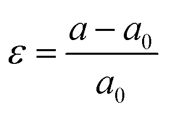
We have considered various heterostructures of MX2 materials. The M elements include Mo, W, Cr, Ir, Ni, Pt, Ru, and Ti, while the X elements include Se, S, Te, and O. Twelve heterostructures are considered in this study, namely MoTe2/WTe2, MoS2/WS2, MoS2/NiS2, MoS2/RuS2, MoS2/PtS2, WS2/NiS2, MoTe2/WSe2, WS2/CrS2, MoTe2/WS2, MoS2/TiO2, MoS2/IrO2, and MoS2/WTe2. The values of strain applied to the hetero-bilayers are reported as  , where a and a0 represent the strained and unstrained lattice constants, respectively. Each model geometry consists of 246 atoms in the unit cell. In this study, we have utilized the A–B stacking configuration and the interlayer distance 3.33 Å, except for the analysis presented in Fig. 6 (both A–B and A–A stacking) and Fig. 7 (distances 3.33 Å and 2.64 Å.) All density functional theory (DFT) calculations are performed with the SIESTA package,46,47 by using the van der Waals density functional (vdW-DF2) exchange functional.48,49 After benchmarking, we choose a double polarized basis set, and we fix the kinetic energy cutoff to 700 eV, and the sampling of the Brillouin zone with a 11 × 11 × 1 Monkhorst–Pack mesh. A vacuum slab separation is used to eliminate the interaction of neighboring layers. All structures are relaxed with the conjugate gradient algorithm until the forces on the atoms are less than 0.01 eV Å−1 and the electronic energy convergence was 10−5 eV. The electron transport properties were calculated self-consistently using the TranSIESTA code which integrates the non-equilibrium Green's function (NEGF) method.50 The electron transport system includes the left electrode (L), the central scattering region (C), and the right electrode (R). The semi-infinite left and right electrodes are connected to the central scattering region. We choose gold electrodes thanks to their favorable properties of good ductility and high electrical conductivity as reported in previous computational studies.51,52 The electric current flows across the device under the applied voltage. The Landauer–Büttiker formula was used to calculate the electric current53 which can be found from the integration of the transmission curve as follows:
| | 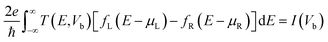 | (1) |
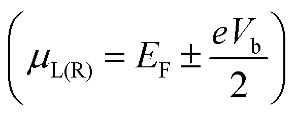
where fL(R), e, I(Vb), μL(R) and ℏ represent the Fermi Dirac distribution function of the left and right electrodes, the electron charge, the electric current under applied bias voltages, the chemical potential of the left and right electrodes and the Planck's constant, respectively. The chemical potential of the two electrodes 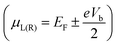 is shifted up and down from the Fermi energy EF, and T(E,Vb) is the transmission coefficient:
| | | T(E,Vb) = Tr[ΓL(E,Vb)G(E,Vb)ΓR(E,Vb)G*(E,Vb)] | (2) |
The retarded and advanced Green's function are represented by G(E,Vb) and G*(E,Vb), respectively. ΓL is the contact broadening function with respect to the left electrode and ΓR is the contact broadening function with respect to the right electrode.54,55 Finally, post-processing tool TBTrans included in the TranSIESTA package was used to calculate the electron transmission function and the electric current. The current–voltage characteristics of each system were obtained under different bias conditions. Various electronic analyses, such as Bader charges, projected density of states and charge density calculations, have been performed to understand the electronic properties of the materials. Additionally, electronic transport calculations have been carried out to identify the best tribo-piezoelectric materials.
3 Results and discussion
3.1 Bader charge analysis
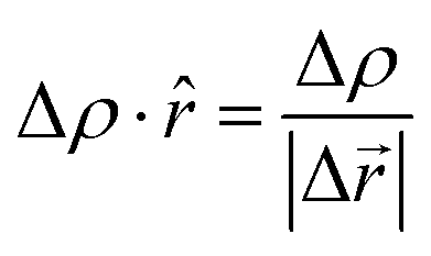
The grid-based Bader analysis algorithm is a method used to divide the charge density grid into Bader volumes. It involves identifying the zero flux surface, which separates one Bader volume from another. Each Bader volume contains the Bader charge associated with a specific atom. To calculate the charges on layers, a post-processing analysis is performed using the on-grid Bader analysis method developed by the Henkelman group and then the charge density gradient in the direction ![[r with combining circumflex]](https://www.rsc.org/images/entities/i_char_0072_0302.gif) is calculated as follows:56–58
is calculated as follows:56–58| |  | (3) |
where Δρ is the change in charge density and Δ![[r with combining right harpoon above (vector)]](https://www.rsc.org/images/entities/i_char_0072_20d1.gif) is the change of distance.
is the change of distance.
The total charge is obtained by summing over all the atoms in the system. Positive values indicate a loss of electrons, while negative values imply a gain of electrons.
To do a first selection of the most promising systems as TENG elements, we select the models which show the largest average charge difference between the two TMD layers in all structures. Specifically, we found large charge difference for the systems MoS/WTe, MoTe/WS, MoS/IrO and MoS/TiO. Since a large charge separation favours the triboelectric activity, we have considered only the systems with the largest charge differences (Table 1). The configurations of these selected heterostructures are shown in Fig. 1.
Table 1 Bader charge analysis of different devices with gold electrodes (unstrained heterostructures)
| MoS/NiS |
Bader charge |
MoS/PtS |
Bader charge |
| MoS |
−0.27 |
MoS |
−0.47 |
| NiS |
0.24 |
PtS |
0.45 |
| Electrode (R) |
0.01 |
Electrode (R) |
0.01 |
| Electrode (L) |
0.02 |
Electrode (L) |
0.03 |
| MoS/RuS |
Bader charge |
MoS/WS |
Bader charge |
| MoS |
−0.18 |
MoS |
0.14 |
| RuS |
0.16 |
WS |
−0.11 |
| Electrode (R) |
0.0 |
Electrode (R) |
0.0 |
| Electrode (L) |
0.02 |
Electrode (L) |
−0.01 |
| MoTe/WSe |
Bader charge |
MoTe/WTe |
Bader charge |
| MoTe |
−0.46 |
MoTe |
0.05 |
| WSe |
0.43 |
WTe |
−0.07 |
| Electrode (R) |
0.01 |
Electrode (R) |
0.0 |
| Electrode (L) |
0.01 |
Electrode (L) |
−0.01 |
| WS/CrS |
Bader charge |
WS/NiS |
Bader charge |
| WS |
−0.29 |
WS |
−0.33 |
| CrS |
0.24 |
NiS |
0.31 |
| Electrode (R) |
0.03 |
Electrode (R) |
0.02 |
| Electrode (L) |
0.02 |
Electrode (L) |
0.03 |
| MoS/WTe |
Bader charge |
MoTe/WS |
Bader charge |
| MoS |
1.61 |
MoTe |
−1.33 |
| WTe |
−1.65 |
WS |
1.31 |
| Electrode (R) |
0.02 |
Electrode (R) |
0.0 |
| Electrode (L) |
0.03 |
Electrode (L) |
0.02 |
| MoS/IrO |
Bader charge |
MoS/TiO |
Bader charge |
| MoS |
−2.50 |
MoS |
−1.59 |
| IrO |
2.47 |
TiO |
1.59 |
| Electrode (R) |
0.03 |
Electrode (R) |
0.02 |
| Electrode (L) |
0.02 |
Electrode (L) |
0.05 |
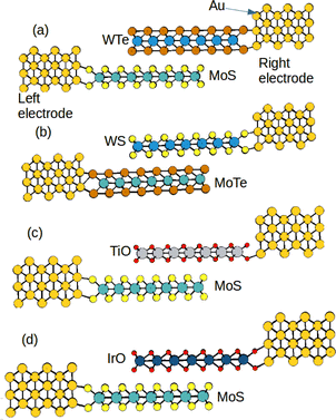 |
| | Fig. 1 Hetero-bilayers of the (a) MoS–WTe/Au system, (b) MoTe-WS/Au system, (c) MoS–TiO/Au system and (d) MoS–IrO/Au system (layer 1 is the bottom layer and layer 2 is the top layer in each heterostructure). | |
The Bader charge analysis results for different heterostructures with strains are presented in Table 2. To determine the charges on layer 1 (the bottom layer), layer 2 (the top layer), and the electrodes, the unstrained structure is used for comparison. The charges on layer 1, layer 2, and the electrodes are obtained by subtracting the charges of the heterostructures from the charges of the unstrained structure. The Bader charge analysis shows that layer 1 accepts a certain number of electrons, while layer 2 loses a corresponding number of electrons. The specific amounts of charge transfer depend on the particular heterostructure. The results show that in MoS/TiO and MoS/WTe heterostructures, layer 1 gains electrons, while layer 2 loses electrons (Table 2). In the case of MoS/IrO and MoTe/WS heterostructures, layer 1 loses electrons, while layer 2 gains electrons. The Bader charge analysis provides valuable insights into the charge transfer between layers in various heterostructures. The observation of increased charge transfer in MoS/IrO, MoS/TiO, MoS/WTe, and MoTe/WS heterostructures under higher applied strain −4% compared to a lower strain −2% is noteworthy. From Table 2, it is observed that under −4% applied strain, MoS/IrO, MoS/TiO, MoS/WTe, and MoTe/WS heterostructures exhibit a slightly higher amount of charge transfer compared to −2% applied strain. The increase in charge transfer under higher applied strain indicates a strain-induced redistribution of charges between the layers. This could be attributed to changes in the interlayer distances, atomic positions, or electronic configurations caused by strain. The fact that MoS/IrO, MoS/TiO, MoS/WTe, and MoTe/WS heterostructures exhibit slightly higher charge transfer under increased strain suggests that these specific combinations of materials are particularly responsive to mechanical deformation. Understanding the nature of charge transfer and the electronic interactions between layers provides insights into how these heterostructures respond to strain. This information is crucial for applications such as nanogenerators, where mechanical stress is harnessed for energy harvesting.
Table 2 Calculated Bader charge values of (MoS–WTe, MoTe-WS and MoS–TiO and MoS–IrO)/Au systems at different strains
| MoS/WTe |
Layers |
−2% |
−4% |
| Layer 1 |
MoS |
−0.09 |
−0.10 |
| Layer 2 |
WTe |
0.06 |
0.12 |
| Electrode |
Right |
0.01 |
−0.04 |
| Electrode |
Left |
0.02 |
0.03 |
| MoTe/WS |
Layers |
−2% |
−4% |
| Layer 1 |
MoTe |
0.04 |
0.05 |
| Layer 2 |
WS |
−0.06 |
−0.08 |
| Electrode |
Right |
0.01 |
0.01 |
| Electrode |
Left |
0.02 |
0.03 |
| MoS/TiO |
Layers |
−2% |
−4% |
| Layer 1 |
MoS |
−0.06 |
−0.10 |
| Layer 2 |
TiO |
0.05 |
0.06 |
| Electrode |
Right |
−0.01 |
0.01 |
| Electrode |
Left |
0.01 |
0.02 |
| MoS/IrO |
Layers |
−2% |
−4% |
| Layer 1 |
MoS |
0.06 |
0.13 |
| Layer 2 |
IrO |
−0.05 |
−0.10 |
| Electrode |
Right |
−0.01 |
−0.02 |
| Electrode |
Left |
−0.02 |
−0.01 |
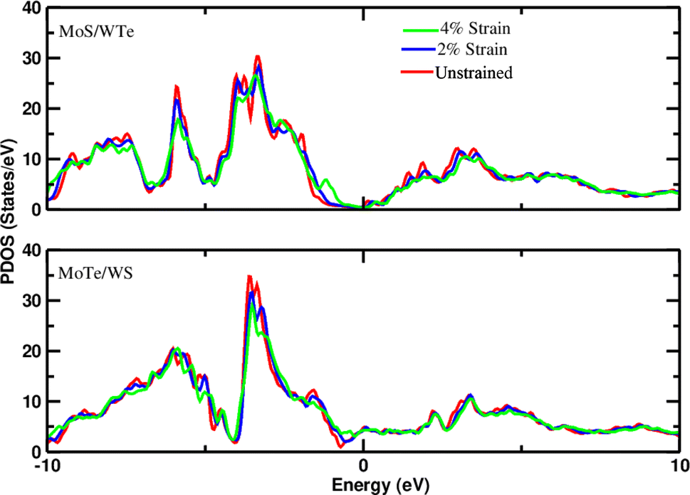
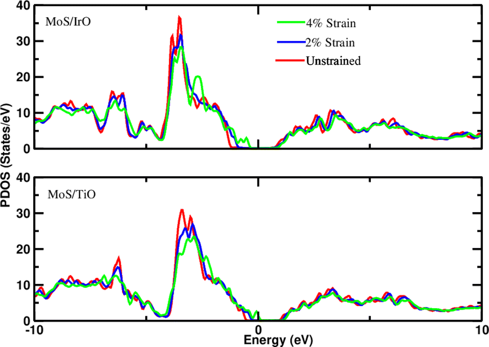
3.2 Density of states and charge density
Density of states measures the number of states at a particular energy level per unit volume for electrons in the conduction band and holes in the valence band. Therefore, the projected density of states (PDOS) of all heterostructures has been investigated to understand the interaction of layers under applied strain. The observation of slight shifts in the d-orbitals of Mo toward the Fermi level with increasing strain, as depicted in the PDOS plots (Fig. 2 and 3), constitutes important insight into the electronic structure of the heterostructures. The slight shift of Mo d-orbitals toward the Fermi level with increasing strain suggests that the applied mechanical deformation affects the electronic orbitals of Mo. This could be due to changes in the interatomic distances or electronic configurations caused by strain. In addition, the observation of minor changes in the band gap under applied strain is also noteworthy. The band gap is a key parameter that determines the material's electrical conductivity. Even minor alterations in the band gap can have significant implications for the material's behavior. The observed electronic structure changes under strain suggest that these heterostructures could find applications in devices that leverage strain sensitivity, such as strain sensors, actuators, or devices based on the piezoelectric effect.
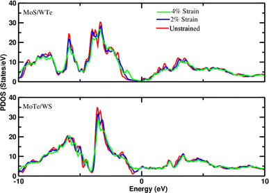 |
| | Fig. 2 Projected density of states of d-orbitals of Mo in the MoS–WTe/Au system and MoTe-WS/Au system at different strains (−2% and −4%).The Fermi level is set to zero. | |
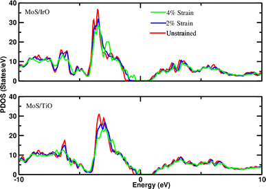 |
| | Fig. 3 Projected density of states of d-orbitals of Mo in the MoS–IrO/Au system and MoS–TiO/Au system at different strains (−2% and −4%). The Fermi level is set to zero. | |
In summary, the slight shifts in Mo d-orbitals and minor changes in the band gap under applied strain highlight the intricate interplay between mechanical deformation and electronic properties in the heterostructures. These findings open avenues for exploring the strain-induced tunability of electronic characteristics for various applications.
The electronic charge density analysis provides valuable insights into the interaction of layers in heterostructures. The charge density plots shown in Fig. 4 depict the distribution of electrons around the atoms in MoTe/WS hetero bilayers. In these plots, the color map serves to differentiate between various levels of electron localization and delocalization. Specifically, the pink color signifies regions with higher charge density, indicating a greater concentration of electrons. On the other hand, the blue color indicates electron delocalization, suggesting that electrons are more spread out in these regions. The cyan color indicates minimal delocalization of electrons, suggesting a weaker interaction or bonding between them, while the red and yellow colors represent regions where there is no significant charge density available.
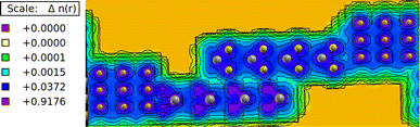 |
| | Fig. 4 Charge density plot of the MoTe/WS hetero bilayer; the isosurface value is 0.05 electron per bohr3. | |
Analyzing the charge density plots, it can be observed that between the layers the electrons are slightly localized, as indicated by the blue color scheme between the layers. This suggests a certain degree of electron confinement or bonding between the layers. Similarly, within the atomic bonds, there is a slight electron localization.
3.3 Current–voltage characteristics
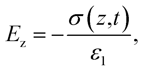
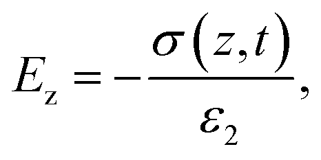
A triboelectric nanogenerator involves the contact electrification between two dielectric layers, which are separated by a gap and connected to electrodes. This process generates electrostatic charges with opposite signs, resulting from the contact. If we assume that the planar size of the dielectric film is much larger than their separation distance, we can calculate the electric field strength between them as follows:59,60| |  | (4) |
| |  | (5) |
| |  | (6) |
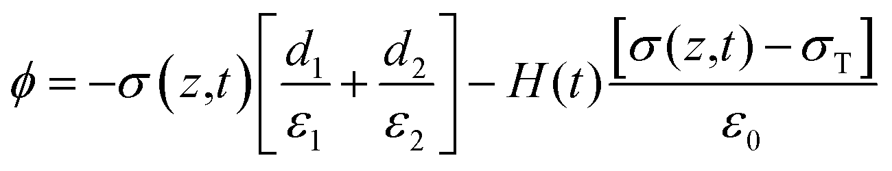
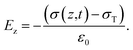
The potential drop between the two electrodes is calculated as follows:
| |  | (7) |
where
σT(
t),
σ(
z,
t),
ε,
H and
d is surface charge density, the density of free electrons on surfaces of the electrodes, permittivity, a function of time and thickness, respectively. The current–voltage (
I–
V) characteristics were studied using the norm equilibrium Green's function (NEGF) technique at various bias voltages (0.0–1.0 V). At each bias voltage, the Landauer–Büttiker formula was utilized with a 0.1 V interval. For the transport setup, Au electrodes were employed on both sides, serving as the left and right electrodes. These electrodes were assumed to be semi-infinite. The scattering region, where the heterostructures were located, was positioned between the left and right electrodes and connected to them in the transport calculations.
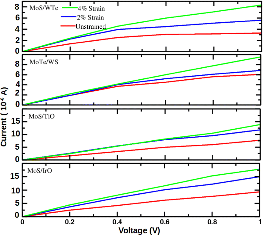
Fig. 5 illustrates the
I–
V characteristics of the MoS/WTe, MoTe/WS, MoS/TiO and MoS/IrO heterostructures. The current response exhibits minor changes and remains within the same order of magnitude in the MoS/WTe and MoTe/WS heterostructures. However, the current response increases as the voltage is raised under applied strain. This behavior indicates rectifying
I–
V characteristics and suggests an improvement in transmission performance, which is consistent with previous research.
61,62
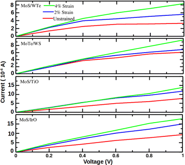 |
| | Fig. 5 Current–voltage characteristics of various TMD bilayers at different strains (−2% and −4%). | |
The I–V curves demonstrate that the current value increases with the increment of the bias voltage, confirming enhanced electron transport transmission across the scattering center. Similarly, Fig. 5 displays the I–V characteristics of the MoS/TiO and MoS/IrO heterostructures, which involve the integration of two-dimensional metal dichalcogenides with other transition metal oxides.
For example, a current which is (1) larger than 10−6 A and at the same time (2) at least ≈2× larger compared to the unstrained bilayer is predicted in the MoS/TiO heterostructure at the −2% strain and a 1.0 V bias voltage or at the −4% strain and a 0.8–1.0 V bias voltage, and in the MoS/IrO heterostructure even at a 0.6–1.0 V bias voltage regardless the strain. On the one hand, the MoS/WTe and MoTe/WS heterostructures exhibit a lower current response, and the latter one also a weaker enhancement of the current response by the strain applied. The substantial enhancement in the current response under strain and bias voltage variations suggests that MoS/TiO and MoS/IrO heterostructures could find applications in devices requiring sensitivity to mechanical strain or specific bias conditions. In summary, MoS/IrO and MoS/TiO hetero-bilayers are unsuitable due to their tendency to exhibit large current flow with increasing voltage, while others like MoS/WTe and MoTe/WS hetero bilayers show promise due to their ability to prevent voltage drop. The observed variations in the current response provide opportunities for optimizing device performance by tailoring strain, bias voltage, or other environmental conditions. Understanding the interplay between these factors is crucial for designing devices with desired electrical characteristics.
Furthermore, it is worth noting that different heterostructures exhibit distinct I–V characteristics, which aligns with findings from previous studies.61 The significant enhancement in the current response under strain and bias voltage variations in the selected heterostructures opens avenues for applications in strain-sensitive and voltage-controlled devices, respectively. These findings contribute to the growing field of heterostructure-based electronic devices with tunable and optimized performance.
Fig. 6 demonstrates that the I–V characteristics for the most promising MoS/WTe and MoTe/WS heterostructures are significantly influenced by their stacking configurations. The A–A stacking shows a higher current response with increasing bias voltage compared to A–B stacking. While the current increases with the bias voltage in both cases, the increase is more significant for the A–A stacking, indicating more efficient electron transport. This can be attributed to better alignment of the electronic states, reduced scattering, and potentially lower interlayer resistance.
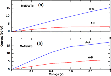 |
| | Fig. 6 Current–voltage characteristics of unstrained (a) MoS/WTe and (b) MoTe/WS bilayers with A–A and A–B stacking. | |
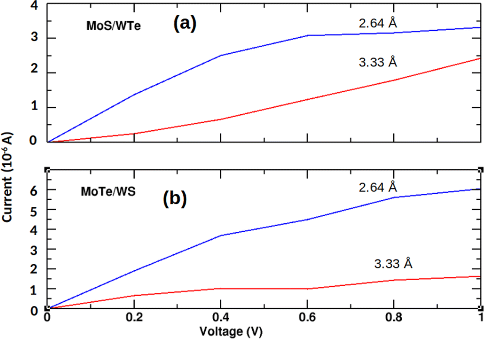
Fig. 7 shows that reducing the interlayer distance in MoS/WTe and MoTe/WS heterostructures from 3.33 Å to 2.64 Å leads to a significant increase in current. While the current once again increases with the bias voltage in both cases, the shorter distance leads to a stronger triboelectric effect, where mechanical interactions at smaller distances convert tribological energy into electrical energy, overcoming the sliding resistance and promoting better electron transport.
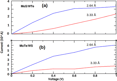 |
| | Fig. 7 Current–voltage characteristic of unstrained (a) MoS/WTe and (b) MoTe/WS bilayers for the interlayer distances 3.33 Å and 2.64 Å. | |
4 Conclusions
We have carried out density functional theory (DFT) studies to investigate the Bader charge analysis, density of states and transport properties of different hetero-bilayers. In the first stage we have evaluated 12 different candidate materials for tribo-piezoelectric nanogenerators, and in the second stage we studied the 4 most promising candidates in detail. Bader charge analysis was conducted to understand the charge transfer between layers in hetero-bilayers under applied strain. The results indicate that the charge transfer between layers increases under applied strain. The interactions of layers in heterostructures under applied strain have been examined. A more significant contribution to the Fermi level has been revealed in strained heterostructures compared to unstrained ones. We have utilized TranSIESTA, a component of the SIESTA package, to calculate electron transport properties. An increase in current response with the applied voltage, with a more significant response under applied strain compared to the unstrained heterostructure has been observed. While MoS/IrO and MoS/TiO hetero-bilayers have been eventually identified as unsuitable due to their tendency to exhibit large current flow with increasing voltage, the non-oxide MoS/WTe and MoTe/WS hetero bilayers show promise due to their ability to prevent voltage drop. Based on the tribo-piezoelectricity observed in TMD bilayers, the compression strain is suggested as a means to enhance the performance of nanogenerators. The understanding of the tribo-piezoelectric effect provides insights into designing materials with improved electronic performance, particularly in nanoelectronic and energy harvesting applications. Generally, piezoelectric nanogenerators convert mechanical energy into electrical energy through the piezoelectric effect. Their performance can be influenced by various factors, including material properties, design, and external conditions like strain. When mechanical strain is applied to piezoelectric materials, it induces a change in their crystal structure. This structural change affects the electronic distribution within the material, leading to charge redistribution. By leveraging strain-induced effects, it is possible to enhance the current output and overall efficiency of these devices. We believe that our findings provide guidelines for further theoretical and experimental research in this field.
Author contributions
JYD: conceptualization, data curation, investigation, methodology, visualization, writing – original draft. JH: writing – review and editing.
Conflicts of interest
There are no conflicts of interest to declare.
Acknowledgements
This work was supported by the project Quantum Materials for Applications in Sustainable Technologies (QM4ST), funded as project No. CZ.02.01.01/00/22_008/0004572 by Programme Johannes Amos Comenius, call Excellent Research.
Notes and references
- H. Cai, Y. Guo, H. Gao and W. Guo, Nano Energy, 2019, 56, 33–39 CrossRef CAS.
- Y. Zi and Z. L. Wang, Apl. Mater., 2017, 5(7) CrossRef CAS.
- Z. L. Wang and J. Song, Science, 2006, 312, 242–246 CrossRef CAS PubMed.
- F.-R. Fan, Z.-Q. Tian and Z. L. Wang, Nano energy, 2012, 1, 328–334 CrossRef CAS.
- S. Sripadmanabhan Indira, C. Aravind Vaithilingam, K. S. P. Oruganti, F. Mohd and S. Rahman, Nanomaterials, 2019, 9, 773 CrossRef PubMed.
- J. Liu, L. Gu, N. Cui, S. Bai, S. Liu, Q. Xu, Y. Qin, R. Yang and F. Zhou, Nanoscale Res. Lett., 2019, 14, 1–10 CrossRef PubMed.
- Q. Liang, X. Yan, Y. Gu, K. Zhang, M. Liang, S. Lu, X. Zheng and Y. Zhang, Sci. Rep., 2015, 5, 9080 CrossRef CAS PubMed.
- J. Seo, Y. Kim, W. Y. Park, J. Y. Son, C. K. Jeong, H. Kim and W.-H. Kim, Appl. Surf. Sci., 2019, 487, 1356–1361 CrossRef CAS.
- H. Ko, Y.-w. Lim, S. Han, C. K. Jeong and S. B. Cho, ACS Energy Lett., 2021, 6, 2792–2799 CrossRef CAS.
- S. S. Won, H. Seo, M. Kawahara, S. Glinsek, J. Lee, Y. Kim, C. K. Jeong, A. I. Kingon and S.-H. Kim, Nano Energy, 2019, 55, 182–192 CrossRef CAS.
- N. Sezer and M. Koç, Nano energy, 2021, 80, 105567 CrossRef CAS.
- X. Zhou, K. Parida, O. Halevi, Y. Liu, J. Xiong, S. Magdassi and P. S. Lee, Nano Energy, 2020, 72, 104676 CrossRef CAS.
- B. Zaarour, L. Zhu, C. Huang, X. Jin, H. Alghafari, J. Fang and T. Lin, J. Ind. Textil., 2021, 51, 297–340 CrossRef CAS.
- V. Jella, S. Ippili, J.-H. Eom, S. Pammi, J.-S. Jung, V.-D. Tran, V. H. Nguyen, A. Kirakosyan, S. Yun and D. Kim,
et al.
, Nano Energy, 2019, 57, 74–93 CrossRef CAS.
- X. Guan, B. Xu and J. Gong, Nano Energy, 2020, 70, 104516 CrossRef CAS.
- J. Chen, S. K. Oh, N. Nabulsi, H. Johnson, W. Wang and J.-H. Ryou, Nano Energy, 2019, 57, 670–679 CrossRef CAS.
- M.-P. Lu, J. Song, M.-Y. Lu, M.-T. Chen, Y. Gao, L.-J. Chen and Z. L. Wang, Nano Lett., 2009, 9, 1223–1227 CrossRef CAS PubMed.
- C.-H. Wang, W.-S. Liao, Z.-H. Lin, N.-J. Ku, Y.-C. Li, Y.-C. Chen, Z.-L. Wang and C.-P. Liu, Adv. Energy Mater., 2014, 4, 1400392 CrossRef.
- T. Charoonsuk, S. Sriphan, C. Nawanil, N. Chanlek, W. Vittayakorn and N. Vittayakorn, J. Mater. Chem. C, 2019, 7, 8277–8286 RSC.
- G. Zhu, C. Pan, W. Guo, C.-Y. Chen, Y. Zhou, R. Yu and Z. L. Wang, Nano Lett., 2012, 12, 4960–4965 CrossRef CAS PubMed.
- S. Wang, L. Lin and Z. L. Wang, Nano Lett., 2012, 12, 6339–6346 CrossRef CAS.
- T. Rodrigues-Marinho, N. Castro, V. Correia, P. Costa and S. Lanceros-Méndez, Materials, 2020, 13, 4980 CrossRef CAS PubMed.
- X. Yang and W. A. Daoud, Adv. Funct. Mater., 2016, 26, 8194–8201 CrossRef CAS.
- S. C. Karumuthil, S. P. Rajeev and S. Varghese, Nano Energy, 2017, 40, 487–494 CrossRef.
- S.-H. Shin, Y. H. Kwon, Y.-H. Kim, J.-Y. Jung, M. H. Lee and J. Nah, ACS Nano, 2015, 9, 4621–4627 CrossRef CAS.
- W. Tang, T. Jiang, F. R. Fan, A. F. Yu, C. Zhang, X. Cao and Z. L. Wang, Adv. Funct. Mater., 2015, 25, 3718–3725 CrossRef CAS.
- J. Zhu, Y. Zhu and X. Wang, Adv. Mater. Interfaces, 2018, 5, 1700750 CrossRef.
- Z. Zheng, H. Yin, B. Wang, Y. Chen, H. Liu and Y. Guo, Nano Energy, 2023, 108, 108236 CrossRef CAS.
- S. Sriphan and N. Vittayakorn, J. Sci.: Adv. Mater. Devices, 2022, 7, 100461 CAS.
- L. Liu, Y. Li, M. Xu, R. Tao, Q. Zhong, X. Yang, S. Lan, J. Xie, G. Chen and Y. Mao,
et al.
, Chem. Eng. J., 2023, 474, 145866 CrossRef CAS.
- J. Seong, B.-U. Bak, D. Lee, J. Jin and J. Kim, Nano Energy, 2024, 122, 109264 CrossRef CAS.
- V. Nguyen and R. Yang, Nano Energy, 2013, 2, 604–608 CrossRef CAS.
- S. Sriphan, T. Charoonsuk, T. Maluangnont, P. Pakawanit, C. Rojviriya and N. Vittayakorn, Adv. Mater. Technol., 2020, 5, 2000001 CrossRef CAS.
- Y. Pang, Y. Cao, M. Derakhshani, Y. Fang, Z. L. Wang and C. Cao, Matter, 2021, 4, 116–143 CrossRef.
- Y. H. Lee, D. H. Kim, Y. Kim, I. Shabbir, M. Li, K. H. Yoo and T. W. Kim, Nano Energy, 2022, 102, 107676 CrossRef CAS.
- H. Wang, H. Feng and J. Li, Small, 2014, 10, 2165–2181 CrossRef CAS.
- M. Gmitra and J. Fabian, Phys. Rev. B, 2015, 92, 155403 CrossRef.
- N. N. Rosman, R. M. Yunus, L. J. Minggu, K. Arifin, M. N. I. Salehmin, M. A. Mohamed and M. B. Kassim, Int. J. Hydrogen Energy, 2018, 43, 18925–18945 CrossRef CAS.
- L. Manamela, J. N. Fru, P. I. Kyesmen, M. Diale and N. Nombona, Front. Chem., 2020, 8, 612418 CrossRef CAS PubMed.
- W. J. Yu, Y. Liu, H. Zhou, A. Yin, Z. Li, Y. Huang and X. Duan, Nat. Nanotechnol., 2013, 8, 952–958 CrossRef CAS PubMed.
- S. A. Svatek, C. Bueno-Blanco, D.-Y. Lin, J. Kerfoot, C. Macías, M. H. Zehender, I. Tobías, P. García-Linares, T. Taniguchi and K. Watanabe,
et al.
, Nano Energy, 2021, 79, 105427 CrossRef CAS.
- T. Mueller, F. N. Xia and P. Avouris, Nat. Photonics, 2010, 4, 297–301 CrossRef CAS.
- W. Wu, L. Wang, Y. Li, F. Zhang, L. Lin, S. Niu, D. Chenet, X. Zhang, Y. Hao and T. F. Heinz,
et al.
, Nature, 2014, 514, 470–474 CrossRef CAS PubMed.
- K. Maity, B. Mahanty, T. K. Sinha, S. Garain, A. Biswas, S. K. Ghosh, S. Manna, S. K. Ray and D. Mandal, Energy Technol., 2017, 5, 234–243 CrossRef CAS.
- C. Wu, T. W. Kim, J. H. Park, H. An, J. Shao, X. Chen and Z. L. Wang, ACS Nano, 2017, 11, 8356–8363 CrossRef CAS PubMed.
- E. Artacho, E. Anglada, O. Diéguez, J. D. Gale, A. García, J. Junquera, R. M. Martin, P. Ordejón, J. M. Pruneda and D. Sánchez-Portal,
et al.
, J. Phys.: Condens. Matter, 2008, 20, 064208 CrossRef PubMed.
- A. García, N. Papior, A. Akhtar, E. Artacho, V. Blum, E. Bosoni, P. Brandimarte, M. Brandbyge, J. I. Cerdá and F. Corsetti,
et al.
, J. Chem. Phys., 2020, 152, 20 Search PubMed.
- J. Klimeš, D. R. Bowler and A. Michaelides, Phys. Rev. B: Condens. Matter Mater. Phys., 2011, 83, 195131 CrossRef.
- S. Li, K. Liu, J. Klimeš and J. Chen, Phys. Rev. Res., 2023, 5, 023018 CrossRef CAS.
- N. Papior, N. Lorente, T. Frederiksen, A. García and M. Brandbyge, Comput. Phys. Commun., 2017, 212, 8–24 CrossRef CAS.
- A. Kole and K. Radhakrishnan, RSC Adv., 2017, 7, 8474–8483 RSC.
- A. Martín-Rodríguez, D. Aravena and E. Ruiz, Theor. Chem. Acc., 2016, 135, 1–10 Search PubMed.
- M. Büttiker, Y. Imry, R. Landauer and S. Pinhas, Phys. Rev. B: Condens. Matter Mater. Phys., 1985, 31, 6207 CrossRef PubMed.
- S. Shin and M. Kaviany, Phys. Rev. B: Condens. Matter Mater. Phys., 2011, 84, 235433 CrossRef.
- C.-H. Yeh and D.-W. Hsieh, FlatChem, 2022, 35, 100418 CrossRef CAS.
- G. Henkelman, A. Arnaldsson and H. Jónsson, Comput. Mater. Sci., 2006, 36, 354–360 CrossRef.
- W. Tang, E. Sanville and G. Henkelman, J. Phys.: Condens. Matter, 2009, 21, 084204 CrossRef CAS PubMed.
- E. Sanville, S. D. Kenny, R. Smith and G. Henkelman, J. Comput. Chem., 2007, 28, 899–908 CrossRef CAS PubMed.
- Z. L. Wang, Nano Energy, 2020, 68, 104272 CrossRef CAS.
- S. Niu, S. Wang, L. Lin, Y. Liu, Y. S. Zhou, Y. Hu and Z. L. Wang, Energy Environ. Sci., 2013, 6, 3576–3583 RSC.
- Y. Zhou, Y. Yang, Y. Guo, Q. Wang and X. Yan, Appl. Surf. Sci., 2019, 497, 143764 CrossRef CAS.
- J. Sun, N. Lin, C. Tang, H. Wang, H. Ren and X. Zhao, Comput. Mater. Sci., 2017, 133, 137–144 CrossRef CAS.
|
| This journal is © The Royal Society of Chemistry 2024 |

 Open Access Article
 This Open Access Article is licensed under a
  * and
Jiri
Houska
* and
Jiri
Houska
 , where a and a0 represent the strained and unstrained lattice constants, respectively. Each model geometry consists of 246 atoms in the unit cell. In this study, we have utilized the A–B stacking configuration and the interlayer distance 3.33 Å, except for the analysis presented in Fig. 6 (both A–B and A–A stacking) and Fig. 7 (distances 3.33 Å and 2.64 Å.) All density functional theory (DFT) calculations are performed with the SIESTA package,46,47 by using the van der Waals density functional (vdW-DF2) exchange functional.48,49 After benchmarking, we choose a double polarized basis set, and we fix the kinetic energy cutoff to 700 eV, and the sampling of the Brillouin zone with a 11 × 11 × 1 Monkhorst–Pack mesh. A vacuum slab separation is used to eliminate the interaction of neighboring layers. All structures are relaxed with the conjugate gradient algorithm until the forces on the atoms are less than 0.01 eV Å−1 and the electronic energy convergence was 10−5 eV. The electron transport properties were calculated self-consistently using the TranSIESTA code which integrates the non-equilibrium Green's function (NEGF) method.50 The electron transport system includes the left electrode (L), the central scattering region (C), and the right electrode (R). The semi-infinite left and right electrodes are connected to the central scattering region. We choose gold electrodes thanks to their favorable properties of good ductility and high electrical conductivity as reported in previous computational studies.51,52 The electric current flows across the device under the applied voltage. The Landauer–Büttiker formula was used to calculate the electric current53 which can be found from the integration of the transmission curve as follows:
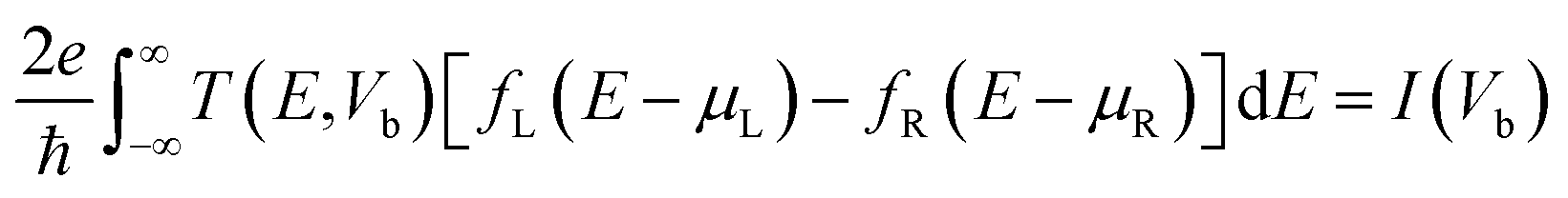
 is shifted up and down from the Fermi energy EF, and T(E,Vb) is the transmission coefficient: