
Percolative phase transition in few-layered MoSe2 field-effect transistors using Co and Cr contacts†
Roshan
Padhan
 a,
Carlos
Garcia
b,
Ralu
Divan
c,
Anirudha V.
Sumant
c,
Daniel
Rosenmann
c,
Sujit A.
Kadam
a,
Akshay
Wali
ac,
Suzanne
Miller
c,
Stephen A.
McGill
*b and
Nihar R.
Pradhan
*a
a,
Carlos
Garcia
b,
Ralu
Divan
c,
Anirudha V.
Sumant
c,
Daniel
Rosenmann
c,
Sujit A.
Kadam
a,
Akshay
Wali
ac,
Suzanne
Miller
c,
Stephen A.
McGill
*b and
Nihar R.
Pradhan
*a
aLayered Materials and Device Physics Laboratory, Department of Chemistry, Physics and Atmospheric Science, Jackson State University, Jackson, MS 39217, USA. E-mail: nihar.r.pradhan@jsums.edu
bNational High Magnetic Field Laboratory, 1800 E. Paul Dirac Dr., Tallahassee, FL 32310, USA. E-mail: mcgill@magnet.fsu.edu
cCenter for Nanoscale Materials, Argonne National Laboratory, 9700 S-Cass Avenue, Lemont, IL-60439, USA
First published on 10th December 2024
Abstract
The metal-to-insulator phase transition (MIT) in two-dimensional (2D) materials under the influence of a gating electric field has revealed interesting electronic behavior and the need for a deeper fundamental understanding of electron transport processes, while attracting much interest in the development of next-generation electronic and optoelectronic devices. Although the mechanism of the MIT in 2D semiconductors is a topic under debate in condensed matter physics, our work demonstrates the tunable percolative phase transition in few-layered MoSe2 field-effect transistors (FETs) using different metallic contact materials. Here, we attempted to understand the MIT through temperature-dependent electronic transport measurements by tuning the carrier density in a MoSe2 channel under the influence of an applied gate voltage. In particular, we have examined this phenomenon using the conventional chromium (Cr) and ferromagnetic cobalt (Co) as two metal contacts. For both Cr and Co, our devices demonstrated n-type behavior with a room-temperature field-effect mobility of 16 cm2 V−1 s−1 for the device with Cr-contacts and 92 cm2 V−1 s−1 for the device with Co-contacts, respectively. With low temperature measurements at 50 K, the mobilities increased significantly to 65 cm2 V−1 s−1 for the device with Cr and 394 cm2 V−1 s−1 for the device with Co-contacts. By fitting our experimental data to the percolative phase transition theory, the temperature-dependent conductivity data show a transition from an insulating-to-metallic behavior at a bias of ∼28 V for Cr-contacts and ∼20 V for Co-contacts. This cross-over of the conductivity can be attributed to an increase in carrier density as a function of the gate bias in temperature-dependent transfer characteristics. By extracting the critical exponents, we find that the transport behavior in the device with Co-contacts aligns closely with the 2D percolation theory. In contrast, the devices with Cr-contacts deviate significantly from the 2D limit at low temperatures.
I. Introduction
The rapid advancement of technology has intensified the demand for more efficient and high-performance devices.1 With the growing use of smartphones, laptops, and data centers, there is an urgent need to address the increasing energy consumption and heat generation associated with these technologies.2 There is an ongoing quest to explore quantum materials with tunable electronic properties for data storage and processing applications. Studying the metal-to-insulator transition (MIT) is particularly significant among various research avenues within two-dimensional (2D) systems.3–6 MIT materials uniquely offer the ability to dynamically and reversibly switch between metallic and insulating states, reducing power consumption and significantly lowering heat generation.3,6,7 This capability is crucial for the next generation of computing, communication, and storage technologies, as it enables faster and more reliable switching mechanisms while enhancing overall device efficiency.3,8 Recent advancements in 2D transistors, such as sub-nm MoS2 FETs, underscore the transformative potential of 2D materials in addressing scaling limitations and mitigating heat dissipation, further emphasizing the importance of studying MIT phenomena in these systems.9 The theoretical foundation for understanding MITs in reduced dimensions was laid by the scaling theory of localization proposed by Abrahams et al.10 which demonstrated that true metallic behavior is absent in two-dimensional disordered systems. Their work revealed how electronic conductance transitions from logarithmic to exponential decay with increasing disorder or reduced system size, providing critical insights into transport phenomena at the nanoscale.Among quantum materials, 2D transition-metal dichalcogenides (TMDCs) are ideal for studying the MIT due to their precise layer-dependent properties, high surface-to-volume ratio, and unique quantum confinement effects.11–13 Their sensitivity to external stimuli allows for more controllable MIT behavior. At the same time, their flexibility and ease of integration into various device architectures enhance their utility in exploring and utilizing MIT phenomena.12,13 Additionally, strong electron correlation effects in these materials make them particularly suited for examining the transition between metallic and insulating states. Among various 2D materials, MoSe2 is particularly interesting due to its pronounced layer-dependent electronic properties, which shift from a direct to an indirect bandgap with changes in thickness.14–16 Its high stability, tunable properties, and compatibility with other 2D materials make it an excellent candidate for studying the MIT.13–15,17 Furthermore, MoSe2 demonstrates superior FET device performance due to its high carrier mobility, excellent electrostatic control, and scalable fabrication, all of which enhance its ability to modulate current flow effectively in response to an applied electric field.6,18–20
This research extends our previous investigation of the MIT in few-layer MoSe2 FETs at low temperatures, demonstrating tunable temperature scaling of the MIT, by using both traditional non-magnetic metallic and ferromagnetic contacts.15 We explored the temperature-dependent transport properties of the 2D MoSe2 devices using Cr and Co-contacts, which showed n-type behavior. The temperature-dependent conductivity data revealed an insulator-to-metal transition as a function of increasingcarrier density, analyzed through theoretical fits to the Fermi-liquid T2-dependent relation. The temperature-dependent 4-terminal conductivities were analyzed using the temperature-dependent percolation theory and showed close agreement with a percolation-driven MIT throughout the studied temperature range for Co-contacts, while the Cr-contacted sample deviated from the predictions of the 2D percolation theory. The extracted critical exponents indicated that devices with Co-contacts closely followed the 2D percolation theory across the temperature range, whereas devices with Cr-contacts deviated from the 2D limit at low temperatures. The temperature-dependent data were also analyzed to understand the transport behavior through the Schottky barrier height (SBH). This work revealed the large difference in the SBH between Cr- and Co-contacted MoSe2 devices that may also tune the MIT properties.
II. Results and discussion
MoSe2 crystals were grown using the chemical vapor transport method and characterized before exploring their temperature-dependent transport properties.15 Raman spectroscopy was employed to verify the quality of the crystals. Thin layers of flakes were mechanically exfoliated using blue tape and transferred onto a clean 285 nm thick SiO2 layer deposited on a highly p-doped silicon substrate. The contacts were fabricated using Laser Writer-based optical lithographic techniques, followed by e-beam evaporation (Lesker PVD 250 at a base pressure of 10−8 Torr) of Au (80 nm)/Cr (5 nm) for Au/Cr contacts and Au (80 nm)/Co (10 nm) for Au/Co-contacts. Several devices were also fabricated using a Temescal e-beam evaporator in a clean room environment. The thickness of the MoSe2 layer was 7–15 nm as measured by atomic force microscopy. Fig. 1(a) shows the optical micrograph image of the 7 nm thick MoSe2 FET devices with contacts of 5 nm Cr and 80 nm Au. Fig. 1(b) shows a 7 nm thick MoSe2 device with 10 nm Co and 80 nm Au fabricated on a 285 nm SiO2 substrate deposited on highly p-doped Si. The thicknesses of the devices were measured using a Veeco Dimension Atomic Force Microscope (AFM). The AFM topography and height measurements are shown in the ESI Fig. S1.† The devices were covered with a thin layer of Cytop polymer to protect them from direct contact with the ambient atmosphere. The transport measurements shown in Fig. 1 were carried out using the 2-terminal method and all temperature dependent transport measurements were performed using the 4-terminal method shown in Fig. 2–5 to eliminate the associated resistance of the contacts. We measured the drain-source current (Ids) as a function of the drain-source voltage (Vds) using two terminals as shown in Fig. 1(c and d) for Cr-contact MoSe2 (Cr-MoSe2) and Co-contact MoSe2 (C-MoSe2) FETs at different applied gate voltages (Vbg). We observed the linear I–V curve on both Cr- and Co-contacted devices although they were Schottky contacts due to the thermionic emission process at room temperature. Fig. 1(e and f) shows the transistor characteristic Ids as a function of applied gate voltage Vbg for Cr-MoSe2 and Co-MoSe2 respectively.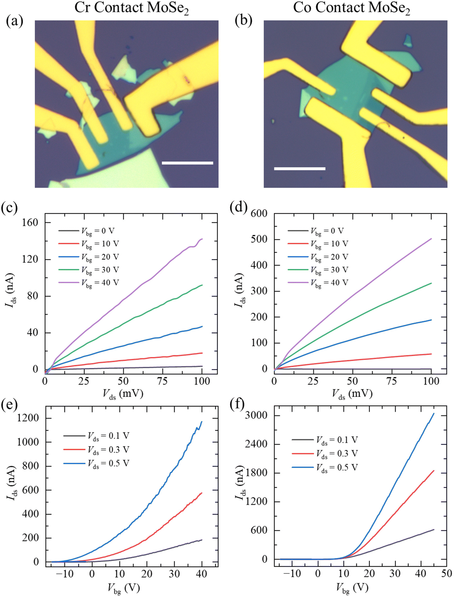 | ||
| Fig. 1 Room temperature FET characterization: (a and b) optical micrograph of MoSe2 devices with Co/Au contact and Cr/Au contact (scale bar: 10 μm), (c and d) basic output characteristics of FET at different back-gate voltages (Vbg) for both Co- and Cr-contact MoSe2 FETs measured at room temperature, (e and f) transfer characteristics of FETs at different source-drain voltages (Vds). | ||
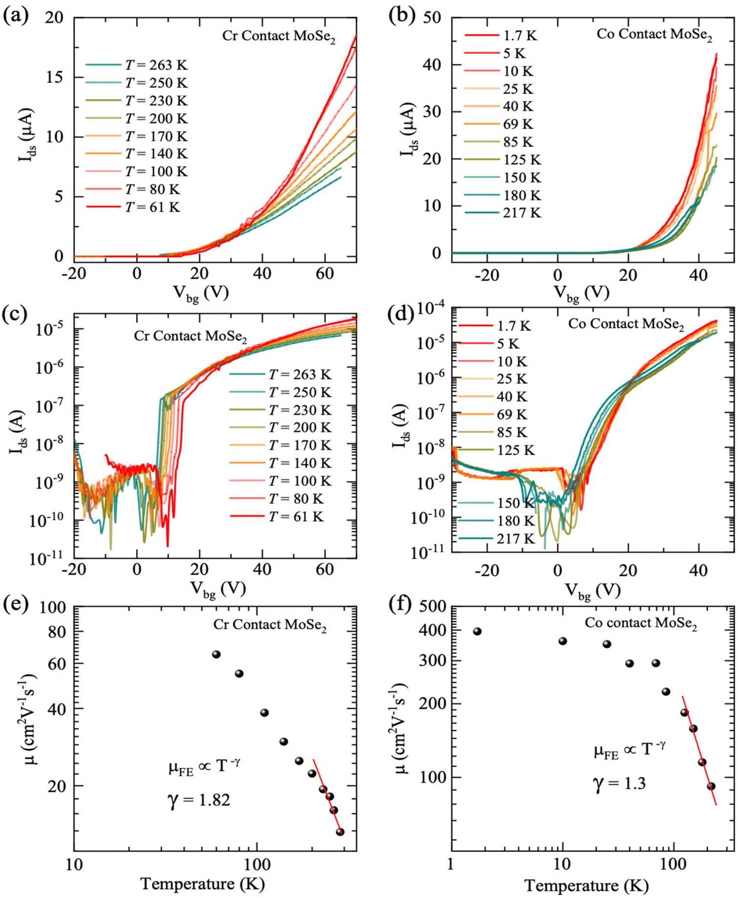 | ||
| Fig. 2 Temperature dependent electrical transport measurement: (a) and (b) transfer characteristics of MoSe2 FET at different temperatures for Cr-contacts and Co-contacts, respectively, measured at Vds = 500 mV, (c) and (d) transfer characteristics of MoSe2 FET at different temperatures for Cr-contacts and Co-contacts in the semi-logarithmic scale, (e) and (f) display the temperature dependent field-effect mobility of the MoSe2 devices for Cr- and Co-contacts, respectively. (The red line indicates the power law fitting for phonon-limited mobility.) | ||
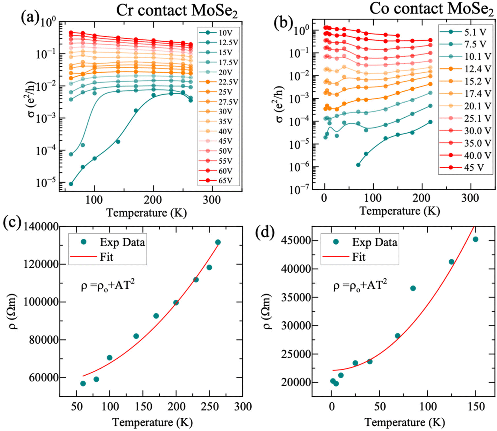 | ||
| Fig. 3 Temperature-dependent conductivity variations: (a and b) T-dependent conductivity at different back-gate voltages for Cr-contacts and Co-contacts, (c and d) Fermi-liquid model fitting of resistivity at a back-gate voltage of 20 V, for Cr-contacts and Co-contacts. | ||
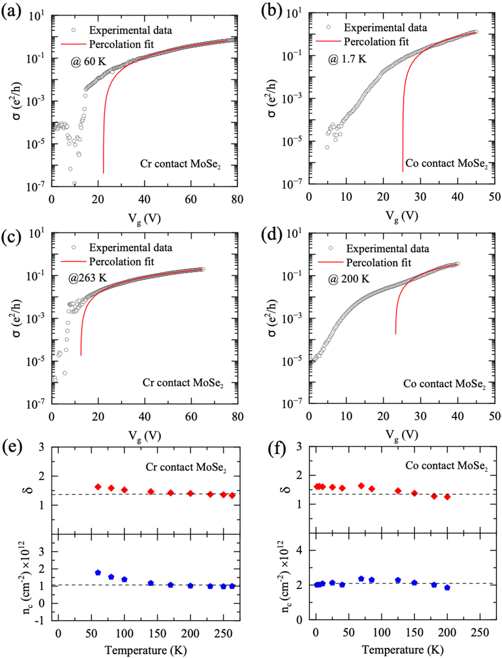 | ||
| Fig. 4 Percolation type phase transition model: the percolation fitting of the conductivity variation data with respect to back-gate voltage at various temperatures (a and c) for Cr-contacted and (b and d) for Co-contacted MoSe2 devices. (e and f) The extracted values of the critical exponent and critical carrier density for Cr-contacts and Co-contacts in the above fitting at different temperatures. | ||
 | ||
| Fig. 5 Schottky barrier height calculation: (a and b) Arrhenius plot for Cr-contacts and Co-contacts at different back-gate voltages, (c and d) activation energy as a function of the back-gate voltage for both contact types (Schottky barrier height was extracted from the curve). | ||
The drain current appears higher in the Co-MoSe2 device compared to the Cr-MoSe2 device for devices with the same thickness of MoSe2, which indicates that the Co-contact could be better than the Cr-contact on MoSe2. The extracted field effect mobilities using the Si-MOSFET formula for 2-terminal devices, 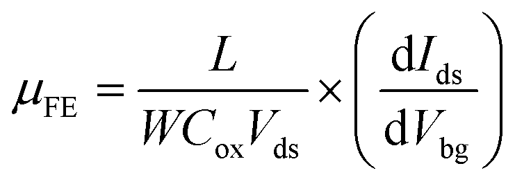 , yields mobility values of 6.5 cm2 V−1 s−1 and 15.2 cm2 V−1 s−1 for Cr-MoSe2 and Co-MoSe2 respectively. The parameter L is the channel length between two current contacts where Vds was applied and current was measured on the same outer (current) contacts. Cox = 11
![[thin space (1/6-em)]](https://www.rsc.org/images/entities/char_2009.gif) :505 × 10−9 F cm−2 is the capacitance/unit area between the gate and the channel for a 285 nm layer of SiO2. Cox = εoεr/d, εr = 3.9 for SiO2 and d = 300 nm. We also measured the four-terminal transport measurements for these devices shown in the ESI Fig. S2.† Fig. S2(a and b)† present the Idsvs. Vbg values of the Cr-MoSe2 and CoMoSe2 devices. The four-terminal mobility values are extracted using the MOSFET relation
:505 × 10−9 F cm−2 is the capacitance/unit area between the gate and the channel for a 285 nm layer of SiO2. Cox = εoεr/d, εr = 3.9 for SiO2 and d = 300 nm. We also measured the four-terminal transport measurements for these devices shown in the ESI Fig. S2.† Fig. S2(a and b)† present the Idsvs. Vbg values of the Cr-MoSe2 and CoMoSe2 devices. The four-terminal mobility values are extracted using the MOSFET relation 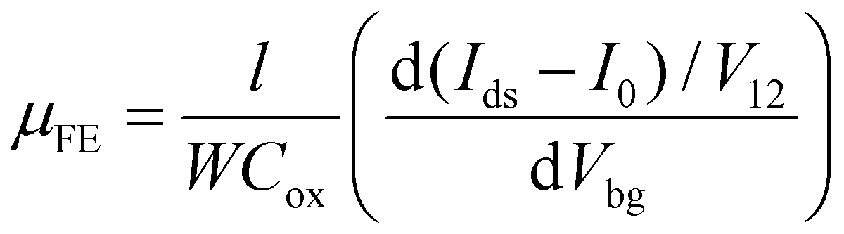 , where l is the channel length of the devices between two voltage contacts (inner contacts in 4-terminal measurements), which was 9.5 μm for the Cr-contact device and 8 μm for the Co-contact device. W is the width of the channel of the devices and the values are 5.4 μm for Cr and 4.78 μm for Co-contacts. Cox is the gate capacitance as stated before and I0 is the current in the subthreshold regime. V12 is the voltage sense between two voltage contacts (inner contacts) in 4-terminal measurements. The value of
  was extracted from the slope of the Ids curve in the linear region. In both cases, μFE increased with decreasing temperature.6,21–25 We found that the field effect mobilities at room temperature of these devices increased to 16 cm2 V−1 s−1 and 45.5 cm2 V−1 s−1 for Cr-MoSe2 and Co-MoSe2 FETs in 4-terminal measurements.
Fig. S2(c and d)† show comparison plots of 2- and 4-terminal measurements of transport curves from where we extracted the contact resistance of the device using the relation 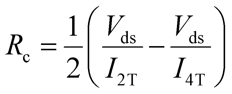 , where I2T and I4T are the drain currents measured from the 2- and 4-terminal configurations respectively. The contact resistances shown in Fig. S2(e and f)† suggest a higher value in the Cr-MoSe2 FET compared to that in the Co-MoSe2 FET. The Rc values for the Cr-MoSe2 and Co-MoSe2 devices are 3 MΩ, 2.7 MΩ (at Vg = 15 V), 1.6 MΩ, 1.2 MΩ (at Vg = 20 V) and 600 KΩ, 200 KΩ (at Vg = 35 V). This could explain why the Co-MoSe2 device performs better than the Cr-MoSe2 FET. Our aim was to explore the temperature-dependent transport behavior of the FETs based on these two different metal contacts and how the conductivities could be tuned as a function of applied gate voltage (i.e., charge carrier density). The conductivities revealed the intrinsic behavior of the MoSe2 when analyzed with temperature-dependent scaling. We measured another set of devices for a temperature dependent study as described below. Fig. 2(a) and (b) display the four-terminal drain-source current, Ids, as a function of back gate voltage, Vbg, at several different temperatures under a constant drain-source voltage of Vds = 500 mV for the devices with Cr- and Co-contacts, respectively. The device showed n-type FET behavior, similar to earlier reports on MoSe2-based FET devices.15,26 The threshold voltage was ∼20 V for both devices, and at Vbg = 0 V, a charge carrier density of n ≈ 1.59 × 1012 cm−2 was induced in the MoSe2 channel. The semi-logarithmic scaled Ids values as a function of Vbg are shown in Fig. 2(c and d) for both Cr- and Co-contacted devices. The observed ON/OFF current ratio of ∼105 showed the comparable performance of the previously reported multilayered TMDC-based devices.15,23,27,28Fig. 2(e and f) display the extracted field-effect mobilities as a function of temperature for Cr- and Co-contacted devices. The field-effect mobilities were extracted from the semiconducting MOSFET relation as explained before where l is the channel length of the devices between two voltage contacts (9.5 μm for the Cr-contact device and 8 μm for the Co-contact devices) and W is the width of the fabricated devices (5.4 μm for Cr and 4.78 μm for Co-contact devices). As shown in Fig. 2(e), for the Cr-contacted device, μFE was determined to be 16 cm2 V−1 s−1 at 263 K and 65 cm2 V−1 s−1 when cooled to 61 K. In contrast, the field-effect mobility for the Co-contacted FET (Fig. 2(f)) was 92 cm2 V−1 s−1 at 217 K and increased to 394.8 cm2 V−1 s−1 when cooled to 1.7 K. Such a difference in mobility for the Co-contacted MoSe2 device demonstrates the significance of using a suitable contact with a high charge injection capacity. Furthermore, cobalt is ferromagnetic, and spin current injection could be another factor that could potentially lead to a reduction in scattering mechanisms through spin–orbit coupling, thereby indirectly enhancing mobility by mitigating certain types of electron scattering events in the Co-MoSe2 device. The mobility obtained is considerably higher than those previously reported for MoSe2-based field-effect transistors with traditional metal contacts.29–31 Furthermore, for both types of contacts, these devices showed strongly T-dependent mobilities, indicating phonon and impurity scattering. At lower temperatures, the phonon scattering of the sample was minimized, resulting in electron mobility being limited by the scattering by impurities and crystal defects. In general, electron–phonon (e–ph) scattering plays a key role in carrier mobility near room temperature.32,33 Longitudinal optical (LO) phonon scattering limits the intrinsic mobility of most transition metal dichalcogenides, while for MoS2 and WS2, the mobility is limited by longitudinal acoustic (LA) phonon scattering.32
Following the phonon scattering theory, we fitted the T-dependent mobility to the power law, i.e., μFE ∝ T−γ, where γ = the phonon scattering exponent. The γ value for the Cr-contacted MoSe2 FET was 1.82, whereas it was 1.3 for the Co-contacted MoSe2 FET. The smaller γ for the Co-contacted MoSe2 FET is associated with a comparatively lower phonon scattering than in the Cr-contacted device. Below 70 K, the phonon scattering is minimized; however, scattering due to impurity and defects states, carrier localization, and the Schottky barrier leads to saturation in the T-dependent mobility. The Co-contacted device showed the highest mobility, ∼400 cm2 V−1 s−1 between 10 and 2 K. Similar T-dependent mobility was reported on MoSe2 FETs fabricated on a SiO2/Si substrate.15
Fig. 3 displays a deeper analysis of the temperature-dependent conductivities of the Cr- and Co-contacted MoSe2 devices. The quantized conductivity (σ) was calculated from the temperature dependent Idsvs. Vbg graph using the relation  , where e is the charge of the electron and h is Planck's constant. The 4-terminal conductivity as a function of temperature at several applied back gate voltages is depicted in Fig. 3(a) for the Cr-contacted MoSe2 FET. This device showed typically semiconducting behavior below Vg = 27.5 V, i.e., σ decreased with decreasing temperature. Conversely, above an applied gate voltage of 27.5 V, the device showed metallic behavior, i.e., σ increased with decreasing temperature. This indicates that upon injecting a high carrier density, the metallic phase emerged from the insulating phase at low temperatures. We also performed a similar T-dependent conductivity analysis for the Co-contacted device at different gate voltages (5.1–45 V) as depicted in Fig. 3(b). In this case, the transition from metallic to insulating behavior was observed at a comparatively lower back gate voltage of 20.1 V. To elucidate the nature of the phase transition, we renormalized the T-dependent conductivity plot with critical conductivity (σc), acquired from the transition point (Vbg = 27.5 V for Cr-contacts and Vbg = 20.1 V for Co-contacts) as shown in the ESI† and then scaled it with the temperature parameter To (ESI Fig. S3†). However, the temperature scaling failed similarly to the previously reported Cr-contact.15 However, our temperature dependent scaling of the conductivity and critical exponent more closely matched the percolation type of phase transition as discussed below. According to the Fermi-liquid model of conductors, resistivity (ρ = σ−1) is related to temperature through the relation ρ = ρ0 + AT2, where ρ0 is the resistivity at 0 K. To verify the metallic behavior at higher gate voltages, we evaluated the resistivity of the channel as a function of temperature. Fig. 3(c) shows the resistivity of Cr-contacted MoSe2 at an applied back gate voltage Vbg = 45 V, and Fig. 3(d) shows the resistivity of the Co-contacted device at Vbg = 65 V. In both cases, the data fit the Fermi-liquid equation well, as indicated by the red line of the plot. A similar metallic conductivity was observed in ReS2 where the resistivity was fitted with the Fermi-liquid T2 dependent equation throughout the temperature range at higher carrier densities or applied gate voltages.34 This theoretical fitting shows the hallmark of metallic behavior of the MoSe2 FET.
We analyzed the temperature-dependent conductivities with the percolation model, and the data are shown in Fig. 4. The temperature-scaled percolation model formulates the relation between conductivity (σ) and the carrier density (n) as σ = A(n − nc)δ, where nc is the critical carrier density beyond which the carriers can form a percolating path in the random network of charged carriers between the source and the drain.22,35 From the theoretical predictions, δ = 1.33 for 2D percolation.15,19,22,36 The density of charge carriers induced at the interface can be controlled by applying the back gate voltage. The induced carriers can be obtained from the relation n = Cox × Vbg/e; hence the percolation prediction for conductivity can be written in terms of Vbg as σ = (A × Cox/e)(Vbg − Vc)δ, where Vc is the critical back gate voltage. We fitted all the temperature-dependent curves with the percolation fits, and two of those fits are shown in Fig. 4(a and c) for the Cr-contacted MoSe2 device. Similarly, the percolation fits for the Co-contacted MoSe2 device are shown in Fig. 4(b and d). More temperature dependent percolation fits are shown in the ESI Fig. S4 and S5.† We extracted the critical exponents δ and Vc from which the critical carrier density nc was calculated. The δ and nc values were plotted as a function of temperature and are shown in Fig. 4(e) and (f), respectively, for Cr- and Co-contacted MoSe2 devices. For the Cr-contacts, the critical exponent lies almost between 1.33 and 1.4, which is the theoretical predicted value of a 2D percolation phase transition, δ = 1.33. The δ value deviated from the theoretical prediction when the device was cooled below 100 K reaching 1.63 at 61 K. For Cr-contacts, the critical carrier density (nc) showed a slight increase with decreasing temperature while the Co-contacted device showed almost temperature independent carrier density. Due to the low contact resistance (Rc) in the Co-contact device, the current (or conductivity) values showed saturation at such applied gate voltages compared to the high contact resistance in the Cr-contacted device as we decreased the temperature. The Idsvs. Vg data in Fig. 2(a–d) show that the conductivity values in the Co-contacted device were nearly four times higher than those in the Cr-contacted device. Thus, the carrier density was still increasing with temperature in the Cr-contact compared to the Co-contact device. This behavior suggests that Co-contacts provide a more efficient carrier injection mechanism, even at low temperatures, leading to constant nc values. These differences reflect the distinct interaction of Cr and Co with MoSe2, likely arising from variations in their work functions, interface chemistry, and surface roughness. Previously, Pradhan et al.15 reported that the value becomes ∼2 at 5 K.2 However, by changing this contact to Co, we have achieved a consistent value near the theoretical predicted value even at low temperatures down to 1.7 K. The constant term, A, depends upon factors like contact resistance (Rc), surface roughness, and the measurement method (i.e., 4-wire/2-wire measurement). Hence, we also found different values of A in the fabricated MoSe2 devices by changing the type of contact. From percolation fitting, the value of A was found to be 0.01 for the Cr-contacts and 0.001 for the Co-contacts.
The obtained critical carrier densities for both Cr- and Co-contacted MoSe2 as a function of temperature are displayed in Fig. 4(e) and (f). For Cr-contacts we obtained the average critical carrier density nc ≈ 1 × 1012 cm−2 (dashed line in Fig. 4e). In contrast, a higher nc of ∼2 × 1012 cm−2 was achieved in the Co-contacted MoSe2 FET.
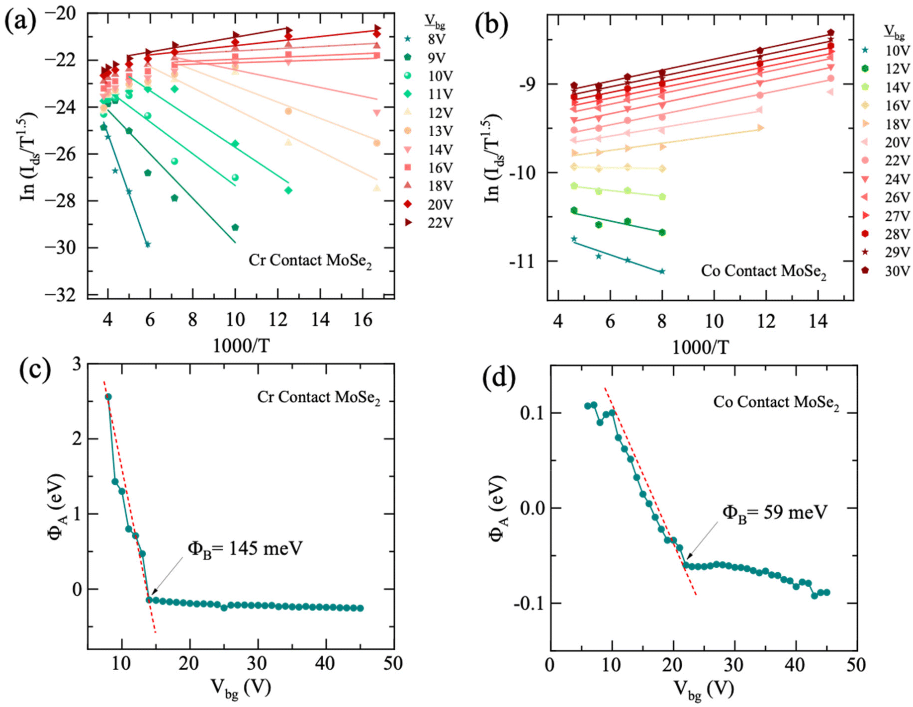
So far, from the above discussion of our conductivity analysis, the Co-contacted MoSe2 device showed a stable 2D percolative phase transition and much higher charge carrier mobility than the Cr-contacted device. To further examine the stability of the Co/MoSe2 interface and analyze the carrier injection from metal to semiconductor, we extracted the Schottky barrier height (SBH) for both types of contacts. The SBH was extracted from the temperature-dependent transfer characteristics of a 2D FET using the following Arrhenius equation for thermionic emission in a 2D system:6,27,37,38

III. Conclusion
In this report, we have demonstrated how different metal contacts with varying Schottky barrier heights can tune the low-temperature transport properties, showing significant differences in electron density and percolative transport behavior. Magnetic contacts could be best suited for exploring and understanding the intrinsic phase transition of 2D semiconductor-based devices. The observed 2D percolation-driven MIT is consistent throughout the temperature range we studied using Co-contacts, which provided a low Schottky barrier height compared to traditional metal contacts, such as chromium. Although the intrinsic mechanism could be the same in both types of contacts, the ferromagnetic Co-contact tends to inject a higher carrier density than the Cr-contacts. This study will influence the exploration of intrinsic MIT behavior in low dimensional materials, particularly 2D materials, and paves the way for their implementation in novel quantum devices.Data availability
The raw data for this article including picture and experimental data of current vs. gate voltage, conductivity vs. temperature and other data presented in the manuscript are available upon request from Dr Nihar R. Pradhan. The data in this manuscript included in the ESI are also available upon request from Dr Nihar R. Pradhan.Conflicts of interest
There are no conflicts to declare.Acknowledgements
This work was carried out at Jackson State University, Argonne National Laboratory, IL, USA and the National High Magnetic Field Laboratory, FL, USA. Funding was provided by the U.S. Department of Energy, Office of Science, Office of Basic Energy Sciences program under Award Number DE-SC0024072. Use of the Center for Nanoscale Materials, a Department of Energy Office of Science User Facility, was supported by the U.S. DOE, Office of Basic Energy Sciences, under Contract No. DE-AC02-06CH11357. A portion of this work was performed at the National High Magnetic Field Laboratory, which is supported by the National Science Foundation Cooperative Agreements No. DMR-1644779 and DMR-2128556 and the State of Florida.References
- P. Wang, M. Hu, H. Wang, Z. Chen, Y. Feng, J. Wang, W. Ling and Y. Huang, Adv. Sci., 2020, 7, 2001116 CrossRef CAS PubMed.
- Y. Lee, H. Cho, H. Yoon, H. Kang, H. Yoo, H. Zhou, S. Jeong, G. H. Lee, G. Kim, G. T. Go, J. Seo, T. W. Lee, Y. Hong and Y. Yun, Adv. Mater. Technol., 2023, 8, 2201067 CrossRef CAS.
- A. B. Georgescu, P. Ren, A. R. Toland, S. Zhang, K. D. Miller, D. W. Apley, E. A. Olivetti, N. Wagner and J. M. Rondinelli, Chem. Mater., 2021, 33, 5591–5605 CrossRef CAS.
- N. Ali, M. Lee, F. Ali, T. D. Ngo, H. Park, H. Shin and W. J. Yoo, ACS Appl. Mater. Interfaces, 2023, 15, 13299–13306 CrossRef CAS PubMed.
- S. Zhang and G. Galli, npj Comput. Mater., 2020, 6, 170 CrossRef CAS.
- M. A. Hoque, A. George, V. Ramachandra, E. Najafidehaghani, Z. Gan, R. Mitra, B. Zhao, S. Sahoo, M. Abrahamsson, Q. Liang, J. Wiktor, A. Turchanin, S. Kubatkin, S. Lara-Avila and S. P. Dash, npj 2D Mater. Appl., 2024, 8, 55 CrossRef CAS.
- A. Hoffmann, S. Ramanathan, J. Grollier, A. D. Kent, M. J. Rozenberg, I. K. Schuller, O. G. Shpyrko, R. C. Dynes, Y. Fainman, A. Frano, E. E. Fullerton, G. Galli, V. Lomakin, S. P. Ong, A. K. Petford-Long, J. A. Schuller, M. D. Stiles, Y. Takamura and Y. Zhu, APL Mater., 2022, 10, 070904 CrossRef CAS.
- Y. J. Lee, Y. Kim, H. Gim, K. Hong and H. W. Jang, Adv. Mater., 2024, 36, 2305353 CrossRef CAS PubMed.
- H. Li, Q. Li, Y. Li, Z. Yang, R. Quhe, X. Sun, Y. Wang, L. Xu, L. Peng, H. Tian, C. Qiu and J. Lu, Adv. Funct. Mater., 2024, 34, 2402474 CrossRef CAS.
- E. Abrahams, P. W. Anderson, D. C. Licciardello and T. V. Ramakrishnan, Phys. Rev. Lett., 1979, 42, 673–676 CrossRef.
- S. Ahn and S. Das Sarma, Phys. Rev. B, 2022, 105, 115114 CrossRef CAS.
- C. Zhang, S. Kc, Y. Nie, C. Liang, W. G. Vandenberghe, R. C. Longo, Y. Zheng, F. Kong, S. Hong, R. M. Wallace and K. Cho, ACS Nano, 2016, 10, 7370–7375 CrossRef CAS PubMed.
- B. H. Moon, Emergent Mater., 2021, 4, 989–998 CrossRef CAS.
- Z. Zhao, H. Zhang, H. Yuan, S. Wang, Y. Lin, Q. Zeng, G. Xu, Z. Liu, G. K. Solanki, K. D. Patel, Y. Cui, H. Y. Hwang and W. L. Mao, Nat. Commun., 2015, 6, 7312 CrossRef CAS PubMed.
- N. R. Pradhan, C. Garcia, B. Chakrabarti, D. Rosenmann, R. Divan, A. V. Sumant, S. Miller, D. Hilton, D. Karaiskaj and S. A. McGill, Nanoscale, 2023, 15, 2667–2673 RSC.
- Y. Liu, N. O. Weiss, X. Duan, H.-C. Cheng, Y. Huang and X. Duan, van der Waals heterostructures and devices, Nat. Rev. Mater., 2016, 1, 16042 CrossRef CAS.
- R. K. Ghosh and S. Datta, in 2016 International Conference on Simulation of Semiconductor Processes and Devices (SISPAD), 2016, pp. 93–96.
- D. Zhou, Y. Zhou, C. Pu, X. Chen, P. Lu, X. Wang, C. An, Y. Zhou, F. Miao, C. H. Ho, J. Sun, Z. Yang and D. Xing, npj Quantum Mater., 2017, 2, 19 CrossRef.
- N. R. Pradhan, D. Rhodes, Y. Xin, S. Memaran, L. Bhaskaran, M. Siddiq, S. Hill, P. M. Ajayan and L. Balicas, ACS Nano, 2014, 8, 7923–7929 CrossRef CAS PubMed.
- D. Zhang, C. Wen, J. B. Mcclimon, P. Masih Das, Q. Zhang, G. A. Leone, S. V. Mandyam, M. Drndić, A. T. C. Johnson Jr. and M.-Q. Zhao, Adv. Electron. Mater., 2021, 7, 2001219 CrossRef CAS PubMed.
- B. Radisavljevic and A. Kis, Nat. Mater., 2013, 12, 815–820 CrossRef CAS PubMed.
- S. Das Sarma, M. P. Lilly, E. H. Hwang, L. N. Pfeiffer, K. W. West and J. L. Reno, Phys. Rev. Lett., 2005, 94, 136401 CrossRef CAS PubMed.
- S. K. Mallik, R. Padhan, M. C. Sahu, S. Roy, G. K. Pradhan, P. K. Sahoo, S. P. Dash and S. Sahoo, ACS Appl. Mater. Interfaces, 2023, 15, 36527–36538 CrossRef CAS PubMed.
- V. Podzorov, M. E. Gershenson, C. Kloc, R. Zeis and E. Bucher, Appl. Phys. Lett., 2004, 84, 3301–3303 CrossRef CAS.
- N. R. Pradhan, D. Rhodes, Q. Zhang, S. Talapatra, M. Terrones, P. M. Ajayan and L. Balicas, Appl. Phys. Lett., 2013, 102, 123105 CrossRef.
- N. R. Pradhan, Z. Lu, D. Rhodes, D. Smirnov, E. Manousakis and L. Balicas, Adv. Electron. Mater., 2015, 1, 1500215 CrossRef.
- S. K. Mallik, R. Padhan, S. Roy, M. C. Sahu, S. Sahoo and S. Sahoo, ACS Appl. Nano Mater., 2024, 7, 4796–4804 CrossRef CAS.
- S. Fathipour, N. Ma, W. S. Hwang, V. Protasenko, S. Vishwanath, H. G. Xing, H. Xu, D. Jena, J. Appenzeller and A. Seabaugh, Appl. Phys. Lett., 2014, 105, 192101 CrossRef.
- A. Allain, J. Kang, K. Banerjee and A. Kis, Nat. Mater., 2015, 14, 1195–1205 CrossRef CAS PubMed.
- X. Cui, E. M. Shih, L. A. Jauregui, S. H. Chae, Y. D. Kim, B. Li, D. Seo, K. Pistunova, J. Yin, J. H. Park, H. J. Choi, Y. H. Lee, K. Watanabe, T. Taniguchi, P. Kim, C. R. Dean and J. C. Hone, Nano Lett., 2017, 17, 4781–4786 CrossRef CAS PubMed.
- A. Dankert, L. Langouche, M. V. Kamalakar and S. P. Dash, ACS Nano, 2014, 8, 476–482 CrossRef CAS PubMed.
- Y. Liu, W. Wu and W. A. Goddard, J. Am. Chem. Soc., 2018, 140, 550 CrossRef CAS PubMed.
- X. Li, J. T. Mullen, Z. Jin, K. M. Borysenko, M. Buongiorno Nardelli and K. W. Kim, Phys. Rev. B: Condens. Matter Mater. Phys., 2013, 87, 115418 CrossRef.
- N. R. Pradhan, A. McCreary, D. Rhodes, Z. Lu, S. Feng, E. Manousakis, D. Smirnov, R. Namburu, M. Dubey, A. R. Hight Walker, H. Terrones, M. Terrones, V. Dobrosavljevic and L. Balicas, Nano Lett., 2015, 15, 8377–8384 CrossRef CAS PubMed.
- L. A. Tracy, E. H. Hwang, K. Eng, G. A. Ten Eyck, E. P. Nordberg, K. Childs, M. S. Carroll, M. P. Lilly and S. Das Sarma, Phys. Rev. B: Condens. Matter Mater. Phys., 2009, 79, 235307 CrossRef.
- M. Imada, A. Fujimori and Y. Tokura, Rev. Mod. Phys., 1998, 70, 1039 CrossRef CAS.
- S. Gupta, F. Rortais, R. Ohshima, Y. Ando, T. Endo, Y. Miyata and M. Shiraishi, Sci. Rep., 2019, 9, 17032 CrossRef PubMed.
- N. Kaushik, A. Nipane, F. Basheer, S. Dubey, S. Grover, M. M. Deshmukh and S. Lodha, Appl. Phys. Lett., 2014, 105, 113505 CrossRef.
- S. Lee, A. Tang, S. Aloni and H. S. Philip Wong, Nano Lett., 2016, 16, 276–281 CrossRef CAS PubMed.
- S. Das, H.-Y. Chen, A. V. Penumatcha and J. Appenzeller, Nano Lett., 2013, 13, 100–105 CrossRef CAS PubMed.
- K. F. Mak, J. Shan and D. C. Ralph, Nat. Rev. Phys., 2019, 1(11), 646–661 CrossRef.
- J. Meng, C. Lee and Z. Li, Sci. Bull., 2024, 69(9), 1342–1352 CrossRef CAS PubMed.
- W. Wang, Y. Liu, L. Tang, Y. Jin, T. Zhao and F. Xiu, Sci. Rep., 2014, 4, 6928 CrossRef CAS PubMed.
Footnote |
| † Electronic supplementary information (ESI) available: Results of AFM, temperature scaling of conductivity, and percolation fitting for all temperatures. See DOI: https://doi.org/10.1039/d4nr03986f |
| This journal is © The Royal Society of Chemistry 2025 |