
Rationally tailored passivator with multisite surface-anchors for suppressing ion migration toward air-stable perovskite solar cells†
Dandan
Luo
b,
Dingyu
Xia
b,
Fei
Wang
*a,
Chong
Jia
b,
Qiang
Zhao
cd,
Xinhua
Li
 cd and
Yiqing
Chen
*b
cd and
Yiqing
Chen
*b
aSchool of Physics, Hefei University of Technology, Hefei, Anhui 230009, People's Republic of China. E-mail: wangfei1213@hfut.edu.com
bSchool of Materials Science and Engineering, Hefei University of Technology, Hefei, Anhui 230009, People's Republic of China. E-mail: chenyq63@126.com
cSchool of Mathematics and Physics, Anhui Jianzhu University, Hefei, 230601, China
dAnhui Research Center of Generic Technology in New Display Industry, Hefei, 230601, China
First published on 23rd April 2025
Abstract
Trap states in perovskite films fabricated using the solution method can capture photo-generated carriers, expedite ion migration, and contribute to decomposition of the perovskite layer, thereby emerging as a major threat to the commercialization of perovskite solar cells (PSCs). To address these issues, passivation of the surface traps on perovskite films via molecules with functional groups is proven to be one of the most effective tactics for obtaining high-performance PSCs. Herein, potassium nonafluoro-1-butanesulfonate (KNFBS) molecules with multiple chemical bonds, including multisite F atoms, sulfonic acid groups and K ions, were introduced as surface-anchoring passivators to improve the film quality and passivate trap states. Based on in situ conductive atomic force microscopy (C-AFM) and Kelvin probe force microscopy (KPFM) results, it was found that undercoordinated Pb and I vacancy defects on the surface and grain boundaries (GBs) of perovskite films can be synergistically curtailed via multiple chemical interactions, including Lewis acid–base, hydrogen and ionic bonds. Moreover, the influence of varied ligands on defects and halide ion migration in perovskites as well as the mechanism behind it were extensively explored. Therefore, the KNFBS-treated perovskite films with a more homogeneous surface potential distribution significantly reduced point and vacancy defects and dangling bond density, facilitated charge transfer, exhibited an optimized power conversion efficiency (PCE) of 20.88% and enhanced air stability for the PSCs fabricated and stored in fully open-air conditions. The work has not only elucidated the fundamental mechanisms of ion migration and multisite passivation at the surface and GBs of perovskites but also probes into ligand design strategies for further improving the performance of perovskite photovoltaics.
1. Introduction
Metal halide perovskite materials have developed into a gamechanger in the optoelectronics field owing to their exceptional optoelectronic properties including regulable bandgaps, convenient solution preparation, and high defect tolerance.1–3 A certified power conversion efficiency (PCE) ranging from 3.8% to over 26.1% has been reported for perovskite solar cells (PSCs) in the last decade or so.4,5 However, the impending problem of poor stability has been a bottleneck to further promote the commercial development of PSCs in the photovoltaic field.6 The instability of perovskite materials generally results from their ionic crystal nature and the traps produced during solution-based film preparation. First, the trap states in the bulk and interface of perovskite films, especially between the crystal grains, usually act as carrier recombination centers and subsequently result in defect-induced performance reduction.7,8 Second, research suggests that the performance deterioration of devices can be accelerated because the trap states are the center of instability and can easily induce the degradation of perovskites by the volatile environment, such as light, heat radiation and moisture.9,10 Third, grain boundaries (GBs) rich in a number of traps can serve as ion transport channels and generate serious outcomes, such as aggravation of current hysteresis in J–V characteristics and even reactions with the silver electrodes of PSCs.11,12In view of the previously mentioned problems caused by trap states existing in GBs and the surface of perovskite films, a series of strategies has been undertaken to improve the properties of GBs, including composition, additive, solvent and processing engineering.13–15 Among them, GB additives have been developed to mitigate the trap state via chemically varied anchors including hydrogen bonds, conjugated bonds, etc.16–18 GB passivators usually include electron donor/acceptor molecules, metal ions, Pb-based complexes, quantum dots, ionic liquid, etc.19–24 For example, Lewis-based molecules containing S, N, and O atoms display excellent effects of trap mitigation via reduction of the shallow trap state at GBs because their electron-donating ability can share with the empty 6p orbital on Pb2+ ions of the perovskite.25,26 Alkali metal ions with low site resistances can permeate into the perovskite lattice and exert the dielectric screening effect, resulting in the promotion of grain growth, elimination of I− chelate and subsequent passivation of Frenkel traps at GBs.27,28 Organic optoelectronic molecules such as (phenylsulfonyl)pyrrole (PSP), DMAcPA, etc. chemically anchored on the surface and GBs have been proved to reduce interfacial voids and compositional heterogeneity in the perovskite surface via the formation of a “molecular lock”.29,30
However, there have been varied challenges for the up-to-date trap passivator in GBs. First, it is tough to carry out the in situ characterization to verify the GB agents due to the difficulties of their penetration in the entire GBs. Secondly, the GB passivator can hardly play multifunctional roles to deactivate the trap state resulting from the lack of synergistic design. Thirdly, the elaborate control of non-excess penetration into the perovskite lattice is needed to release GB strain and strengthen the GB structure. Inspired by the above challenges, potassium nonafluoro-1-butanesulfonate (KNFBS) was targeted as a novel anionic surfactant with multi-action sites for use as a GB and surface passivator. The KNFBS additive with three different kinds of chemical anchors, including multi-F atoms, alkali metal K+, and sulfonic acid group S![[double bond, length as m-dash]](https://www.rsc.org/images/entities/char_e001.gif) O can play cooperative roles in GB passivation. Although the passivation effect based on the single functional group is well-known, the synergistic effect included in one GB passivator has rarely been explored. Moreover, it is not clear whether the GB additives have penetrated into GBs and stayed inside. Therefore, a thorough exploration was conducted to provide direct evidence of GBs permeation and subsequently obtain a comprehensive understanding of an underlying mechanism of GB passivation using Kelvin probe microscopy (KPFM) and conductive atomic force microscopy (c-AFM). Profiting from the trap passivation due to the multi-functional groups of KNFBS additives, the champion PCE of KNFBS-treated devices is raised to 20.88% with a high Voc of 1.10 V, Jsc of 24.18 mA cm−2, and FF of 78.81%. In addition, the unencapsulated KNFBS-treated cells can maintain 82% of its initial efficiency in an ambient environment with a relative humidity of 35 ± 5%, while the pristine device declined to 58% after more than 42 d. This study put forward a novel agent for the surface and GB passivation and elucidated the underlying mechanism of suppression of ion migration, which is expected to offer more rational tailoring of multifunctional agents.
O can play cooperative roles in GB passivation. Although the passivation effect based on the single functional group is well-known, the synergistic effect included in one GB passivator has rarely been explored. Moreover, it is not clear whether the GB additives have penetrated into GBs and stayed inside. Therefore, a thorough exploration was conducted to provide direct evidence of GBs permeation and subsequently obtain a comprehensive understanding of an underlying mechanism of GB passivation using Kelvin probe microscopy (KPFM) and conductive atomic force microscopy (c-AFM). Profiting from the trap passivation due to the multi-functional groups of KNFBS additives, the champion PCE of KNFBS-treated devices is raised to 20.88% with a high Voc of 1.10 V, Jsc of 24.18 mA cm−2, and FF of 78.81%. In addition, the unencapsulated KNFBS-treated cells can maintain 82% of its initial efficiency in an ambient environment with a relative humidity of 35 ± 5%, while the pristine device declined to 58% after more than 42 d. This study put forward a novel agent for the surface and GB passivation and elucidated the underlying mechanism of suppression of ion migration, which is expected to offer more rational tailoring of multifunctional agents.
2. Results and discussion
Steady-state (PL) measurements are conducted to evaluate the recombination characteristic of perovskite film based on the distinct configuration of FTO/perovskite and FTO/perovskite/HTM, as plotted in Fig. 1a and b, respectively. It is observed that the PL peaks at 768 nm correspond to all the as-prepared perovskite samples. Beyond that, the intensity of thin film containing 1.5 mg mL−1 KNFBS was approximately five times higher than the reference, indicating more abundant production of light-induced electrons due to the improvement of crystallization and light absorption after KNFBS treatment. The PL intensity of the target films were significantly diminished compared with the control (Fig. 1b), indicating that alleviation of carrier recombination can facilitate electron extraction at the perovskite/HTM interface.31 | ||
| Fig. 1 Steady-state PL spectra based on the active layer (a) without and (b) with the HTL layer. Space-charge-limited current (SCLC) curves of the hole-only devices: (c) control and (d) with 1.5 mg mL−1 KNFB agents. Light intensity-dependent: (e) Voc and (f) Jsc. (g) Mott–Schottky plots. (h) Nyquist plots of EIS in the dark with the corresponding equivalent circuits for fitting in the inset. | ||
X-ray diffraction (XRD) measurements were exerted to explore the effect of KNFBS agents on the crystallinity properties of perovskite film. The XRD results of the perovskite samples are presented in Fig. S1a,† with the peak at 14.0° corresponding to the (100) plane of the perovskites.32 The negligible alteration of the diffraction peak position of the as-prepared samples after KNFBS passivation indicates their similarity in crystal structure. Fig. S1b† presents the full-width-at-half-maximum (FWHM) and peak intensity of the perovskites at 14.0°. Thus, the KNFBS -treated perovskite layer manifests a narrower half-width and higher peak intensity, indicating better crystallization of the as-prepared films with diminished defects.
The UV-visible absorption spectra are conducted to investigate the influence of KNFBS on the perovskites. As shown in Fig. S1c,† the absorbance intensity of KNFBS-added film is higher both in the visible and the infrared region compared with the control sample, which is attributable to the better film quality and enlarged crystal grains (as depicted in Fig. 3a and b). Photon capture and the subsequent current density of the devices can be improved for the higher absorbance intensity of passivated perovskite film. Notably, an undistorted crystal structure of perovskites was confirmed by the insignificant changes in the optical bandgap (Eg) of 1.576 eV calculated by the Tauc plots in the inset.
To estimate the trap density of the as-prepared films, space charge limited current (SCLC) measurements were exerted on hole-only devices in Fig. 1c and d, which were depicted in the logarithmic scale. Three distinct regions were observed at low, intermediate and higher biases, standing for the ohmic, the trap-filled limited and trap-free SCLC region, respectively. Generally, the point of intersection between intermediate and higher biases regions determines the value of trap-filled limit voltage (VTFL).33,34 Subsequently, the trap densities Ntrap can be supposed by the following equation:35
 | (1) |
Apart from Ntrap, the Mott–Gurney law could be exerted to evaluate the carrier mobility (μ) by fitting the J–V curves:
 | (2) |
The relationship between light intensity and Jsc as well as light intensity and Voc was investigated to probe the effect of KNFBS agents on carrier transport and recombination properties. Generally speaking, there are two types of carrier recombination processes. One is single-molecular recombination, referring to the recombination of only one carrier (electron or hole), and the other is biomolecular recombination, referring to the recombination of both electrons and holes during the process. The following power-law behavior was confirmed by the Jsc and light intensity:38
| Jsc = Iα | (3) |
 | (4) |
The built-in voltage (Vbi) of cells can be obtained via the Mott–Schottky plots, in which Vbi is calculated according to the following equation:40
 | (5) |
| KNFBS concentration (mg mL−1) | R s (Ω) | R ct (Ω) | CPE-T | CPE-P | τ n (ms) |
|---|---|---|---|---|---|
| 0 | 32.33 | 91![[thin space (1/6-em)]](https://www.rsc.org/images/entities/char_2009.gif) 059 059 |
2.38 × 10⁻⁸ | 0.97 | 1.75 |
| 0.5 | 29.49 | 137891 |
2.54 × 10⁻⁸ | 0.95 | 2.60 |
| 1.0 | 30.59 | 144742 |
2.16 × 10⁻⁸ | 0.94 | 2.22 |
| 1.5 | 24.41 | 161620 |
2.12 × 10⁻⁸ | 0.96 | 2.77 |
| 2.0 | 38.03 | 136035 |
2.31 × 10⁻⁸ | 0.96 | 2.42 |
Furthermore, EIS was carried out under different bias voltages to explore the rate of ion migration after the introduction of KNFBS agents. Fig. S3a to Fig. S3b† displays Nyquist plots under different bias containing the equivalent circuit model in the inset and the corresponding fitting parameters are summarized in Tables S1 and S2.† Similar to the Rs, Rct and CPE in the equivalent circuit of the middle frequency (MF) region of Fig. 1h, a new fitting element, Ws, represents diffusion impedance at low frequency (LF) region. Recent studies have demonstrated that the signal in HF (high frequency) is consistent with fast electronic processes, while that in LF is consistent with electrochemical processes such as ion diffusion and electrochemical reactions.45 The effect of KNFBS agents on τn was similar to the results displayed in Table 1. Interestingly, when bias voltage increased, a single recombination semicircle was observed in the MF region, indicating that only one type of carrier (electronic) transport is predominant under dark conditions, which is attributed to carrier trapping and surface recombination.46 Based on the calculation of ion diffusion coefficient (Dion), the slope of the Z′′ curve in the image of Z′′ as a function of ω−1/2 in Fig. S3e,† extracted from the spectrum of the LF region in Fig. S3d,† can be used to evaluate the value of the Warburg coefficient: σw. The value of the corresponding slope in Fig. S3e† is directly proportional to the value of σw and  .47 The KNFBS-based device presents a larger value of σwand a reduced value of Dion, indicating suppressed ion migration after the introduction of KNFBS agents.
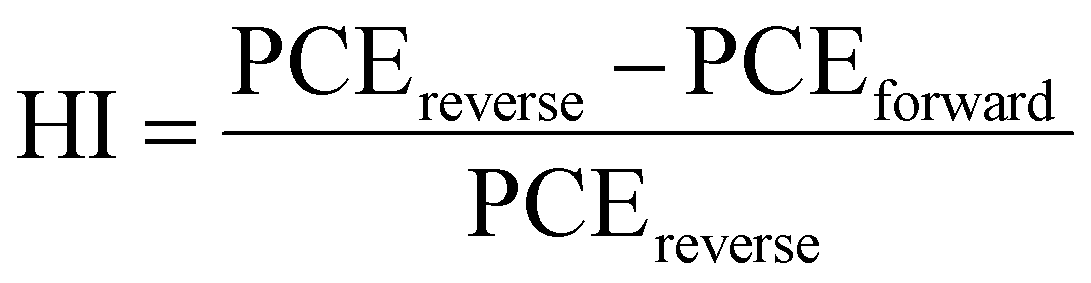
To understand the impact of the concentration of KNFBS on photovoltaic performance, J–V curves of the champion devices based on 0.5, 1, 1.5, and 2 mg mL−1 of KNFBS agents were compared in Fig. 2a and the corresponding photovoltaic characteristics are displayed in Table 2. Compared with the reference device, 1.5 mg mL−1 of KNFBS remarkably raises all the photovoltaic parameters of PSCs: Voc, Jsc, and the fill factor (FF). The best PCE of the reference device was 17.24%, with an Voc of 1.05 V, a Jsc of 22.88 mA cm−2, and an FF of 71.84%. In contrast, the best PSC based on 1.5 mg mL−1 KNFBS agents displayed a PCE of 20.88%, an Voc of 1.10 V, a Jsc of 24.18 mA cm−2, and an FF of 78.81%. The noteworthy increase in Jsc was a result of the enlarged perovskite grain size and a raised visible optical absorption of the film.25 As shown in Fig. S2b and Table S3,† the HI values of the reference and target samples were obtained as 0.22 and 0.13, respectively, using the following equation:48
 | (6) |
 | ||
| Fig. 2 Photovoltaic performance of pristine and KNFBS-treated devices: (a) J–V curves; (b) IPCE curves. (c) Stabilized PCE and Jsc at the maximum power point (MPP) output. Statistical photovoltaic parameter distribution obtained from 30 devices: (d) Jsc; (e) Voc; (f) FF; (g) PCE. | ||
| KNFBS (mg mL−1) | V oc (V) | J sc (mA cm−2) | FF (%) | PCE (%) | |
|---|---|---|---|---|---|
| 0 | Best | 1.048 | 22.88 | 71.84 | 17.24 |
| Average | 1.048 ± 0.015 | 22.71 ± 0.5 | 71.65 ± 2.74 | 17.16 ± 0.87 | |
| 0.5 | Best | 1.071 | 23.96 | 75.01 | 19.24 |
| Average | 1.071 ± 0.012 | 23.83 ± 0.86 | 74.68 ± 3.3 | 18.57 ± 1.68 | |
| 1.0 | Best | 1.095 | 23.88 | 77.23 | 20.19 |
| Average | 1.091 ± 0.019 | 23.54 ± 0.52 | 76.02 ± 4.17 | 19.53 ± 1.3 | |
| 1.5 | Best | 1.096 | 24.18 | 78.81 | 20.88 |
| Average | 1.094 ± 0.015 | 24.13 ± 0.44 | 79.73 ± 4.21 | 20.33 ± 0.97 | |
| 2.0 | Best | 1.085 | 23.65 | 75.71 | 19.42 |
| Average | 1.083 ± 0.019 | 23.53 ± 0.42 | 75.41 ± 3.85 | 19.25 ± 1.38 | |
The diminished hysteresis effect of the cells can be attributable to the successful suppression of ion migration and reduction of defect density via KNFBS addition.
The incident photoelectron conversion efficiency (IPCE) spectrum further verifies the positive impact of KNFBS treatment. As shown in Fig. 2b, the KNFBS-treated sample displays the highest IPCE values, resulting in a raised integrated Jsc from 22.69 to 23.95 mA cm−2, in agreement with the measured Jsc. Additionally, a steady-state PCE and photocurrent density output were tested to evaluate the operational stability of the pristine and KNFBS-treated devices. As shown in Fig. 2c, the steady-state PCE outputs for the reference and KNFBS-treated cell under continuous operation with maximum power point (MPP) tracking were 17.10% and 20.14%, respectively. The photocurrent density output for the reference and KNFBS-treated cell were 20.22 and 23.07 mA cm−2, respectively. Moreover, Fig. 2d–g and Table 2 depict the statistical distribution of Jsc, Voc, FF and PCE values for the 30 different devices; the 0.5, 1.0, 1.5 and 2 mg mL−1 KNFBS added devices deliver average PCEs of 17.16 ± 0.87, 18.57 ± 1.68, 19.53 ± 1.3, 20.33 ± 0.97 and 19.25 ± 1.38%, respectively. The main raised parameters of Voc and FF for the target cell were boosted up to 1.094 ± 0.015 and 79.73 ± 4.21%, respectively, resulting from the enlarged grain size of perovskite.
The effect of KNFBS agents on the morphology of thin films was studied using scanning electron microscopy (SEM). As visualized in Fig. 3a and b, the reference films present some voids, implying a defective film morphology. In contrast, the target films demonstrate compact and homogeneous surface without voids. Fig. 3c and d exhibit the target film with larger average grain sizes (∼360 nm) than the reference one (∼160 nm), signifying diminished GB areas and grain defects. Beyond that, the released stress at perovskite grains and distorted lattice due to the interaction between KNFBS and perovskite is beneficial for high-quality perovskite films. Besides, atomic force microscopy (AFM) was employed to observe its morphology. As depicted in Fig. S4a and S4b,† the surface roughness (RMS) dropped from 12.0 to 9.97 nm after KNFBS treatment. The corresponding 3D diagram manifests that the target film became smoother due to the oriented growth of crystals and diminished defects. The corresponding cross-sectional and top-view SEM images of functional layers (Fig. S5†) manifest a thickness of ∼420 nm for the target film, which is slightly thicker than that of the control film. Meanwhile, a vertical columnar shape was observed in the target layer of Fig. S5b,† which was credited for carrier transport along the perpendicular orientation to the ETL/HTL and inhibition of nonradiative carrier recombination.49
 | ||
| Fig. 3 Top-view SEM images of (a) pristine and (b) KNFBS + perovskite films. Histograms of the grain size of (c) pristine and (d) KNFBS + perovskite films. XPS spectra of control and KNFBS-doped perovskite films: (e) F 1s; (f) Pb 4f and (g) I 3d. (h) FTIR spectra of pure KNFBS passivators, pristine, KNFBS-doped perovskites. (i) NMR spectra of the MAI and mixed MAI + KNFBS in DMSO-d6 solutions. | ||
X-ray photoelectron spectroscopy (XPS) and Fourier transform infrared (FTIR) spectroscopy was conducted to uncover the chemical interaction between KNFBS and perovskite. Fig. 3e and Fig. S6a† indicate the incorporation of F atoms into perovskite films. As shown in Fig. 3f, the Pb 4f peaks of 141.9 eV for Pb 4f5/2 and 137.04 eV for Pb 4f7/2 in the pristine film shift about 0.3 eV toward lower binding energy in the target film (141.6 eV for Pb 4f5/2 and 136.75 eV for Pb 4f7/2), due to an increase in the electronic cloud density. This verifies that SO groups can chelate with the undercoordinated Pb2+ ions in the target film.50 It is noted that there are two weak signals corresponding to the metallic Pb0 cluster in the control film. Generally, the metallic Pb0 cluster, along with the I− and MA+ vacancy defects, are indeed deep-level defects and can exacerbate carrier nonradiative recombination. Thus, the reduced intensity of the Pb0 signals verifies that the under-coordinated Pb2+ has been effectively suppressed by KNFBS additives. Similarly, a significant shift to lower energy can be observed for the peaks of I 3d3/2 and I 3d5/2 in Fig. 3g, resulting from the mitigated I− vacancies via KNFBS passivation in perovskite. The K+ metallicity of KNFBS agents at the surface and GBs strongly chelate with I− ions and can deactivate the I− vacancy defect, thereby resulting in improvement of PCE and diminished I–V hysteresis.51 The XPS spectra of N 1s (Fig. S6b†) also verifies the interaction between KNFBS and perovskite. These comprehensive results can verify that KNFBS passivators exert preferential interaction with perovskite due to the multiple formation of N–H⋯F hydrogen bonds and ionic bonds, leading to the improvement of electrical properties and thereby a synergistic passivation effect toward more efficient PSCs.52
As presented in Fig. 3h, the SO stretching peak of the pristine KNFBS shifted from 1062 cm−1 to a lower wavenumber (1048 cm−1) after KNFBS incorporation.53 The decreased vibrational frequency indicates a strong interaction between the sulfuryl groups of KNFBS and the Pb2+ ions of perovskite. In addition to XPS results, this result can also imply that the oxygen sites in the anions of KNFBS can serve the role of Lewis bases, via the donation of unpaired electrons to the vacant orbitals of Pb2+. Moreover, the strong chemical anchor between KNFBS and perovskite can disassemble the large perovskite colloids in the precursor, leading to the decrease of the perovskite nucleation rate and enlarged perovskite grain size.54
To verify the chemical interactions between KNFBS agents and perovskite, nuclear magnetic resonance (NMR) measurements of 19F and 1H were implemented by dissolving the powders in deuterated DMSO-d6. As displayed in Fig. S6c,† the MAI-KNFBS mixture exhibits an 0.10 ppm increasing chemical shift of the 19F signal, attributed to the deviation of the N–H electronic cloud to KNFBS and the alteration of the shielding effect, which indicates the chelation of F-ions with MA+ and inhibition of the Pb2+ vacancy defect (VPb).55 Besides, after the addition of KNFBS into the MAI sample, the 1H signal of the pristine MAI and MAI-KNFBS mixture was observed to shift from 7.50 to 7.48 ppm (Fig. 3i). The signal belongs to the protons of the NH3+ units of the MA+ moiety, which verifies the formation of N–H⋯F hydrogen bonds. The formation of hydrogen bonds originated from the boosted shielding effect of electrons and increased electron cloud density surrounded by the hydrogen nucleus of NH3+ units.56 Thereby, the F, K+, and SO groups in KNFBS agents can be conducive to the stabilization of the perovskite crystal structure with suppressed Pb2+ and I− vacancies.
Conductive atomic force microscopy (c-AFM) was exerted to visualize not only the distributions of electrical conductivity inner grains and at GBs, but also the traps of the materials in nanoscale, which can elucidate the impact of trap passivation on transport kinetics of charges. As shown in the current images of Fig. 4a and b, the target film reveals a brighter image overall compared with the pristine film, indicating the enhanced conductivity and charge transport of the target film. The overall enhancement in current of the KNFBS-passivated sample is consistent with the more uniform distribution of CPD across the surface (Fig. 5b), and indicates the reduction of trap density at each crystal facet.57 The corresponding line profiles of Fig. 4c displays a lower conductance of the pristine film, which is primarily attributable to the charge loss through defect-induced recombination. Interestingly, the control film shows that the current flowing along the GBs is higher than that the grain interior (GI), confirming that GBs play an advantage in charge gathering and transport. Similarly, the significantly brighter GBs of the target films indicates more efficient separation of the photon-generated carrier at the GBs compared with the GI. Thereby, GBs play an important role in transport channels for the carriers.58 Due to deactivation of defects including I− vacancy and the Pb2+ interstitial at GBs, the traps become shallow and the charge mobility is enhanced, which accounts for the boost in photocurrent at GBs compared with that of GIs. Furthermore, the results can also be credited to an offset of band bending between grains and GBs, which can reduce the barrier height and facilitate spatial charge extraction and accumulation, leading to the promotion of carrier transport across GBs.59 Moreover, local I–V properties of inner grains and along GBs were explored to elucidate the mechanism of notorious hysteresis in PSCs. As shown in Fig. 4d and e, GBs and GI of the control films exhibit pronouncing I–V hysteresis, which can originate from the dominant phenomenon of ion migration and charged defects taking place towards the GI from the GBs where they are rich in defects and dangling bonds.60 On the other hand, the target films exhibit diminished I–V hysteresis due to a reduction of ion migration and trap levels, leading to the alteration of electrical properties and the dynamics of charge trapping/de-trapping in GBs.61
 | ||
| Fig. 4 c-AFM mapping of the currents at perovskite GBs and grains. Current images for (a) the control, (b) KNFBS-doped perovskite films, and (c) current distribution based on random 1D line scanning. Distinct I–V hysteresis at the GI or GBs for (d) the control and (e) KNFBS-doped perovskite films, respectively. | ||
 | ||
| Fig. 5 (a) and (b) Contact potential difference (CPD) image of KPFM mapping. The recorded lines mark the different measured location of GBs. (c) and (d) The profiles based on 1D line scanning of the previous CPD image. (e) and (f) Statistical CPD variation across the GBs based on the corresponding 1D line scanning profiles. The diagrams in the first and second lines are for the control and KNFBS-doped perovskite films, respectively. | ||
In situ Kelvin probe force microscopy (KPFM) was carried out to monitor electrical properties of the target perovskite films after the doped agents. As shown in the potential mapping of Fig. 5a and b, minimized potential discrepancy between individual grains and higher surface potential were displayed for KNFBS-treated perovskite films. The evident variations of surface potential in the control film can originate from the high density of the trap state on the surface.62 Thus, the alleviated variation of contact potential difference (CPD) in the target film implies that the KNFBS passivator can effectively deactivate surface traps of the sample. The homogenization of CPD between the GB and grains of the target samples demonstrates improvement of the junction properties due to changes of surface traps or band alignments at GBs, which accounts for the reduction of Voc loss in the target devices.63 Moreover, Fig. 5b displays that the overall surface potential of the perovskite film after KNFBS treatment is evidently higher than that of the pristine perovskite sample. The CPD applies to the potential discrepancy between the probe tip and film surface, which is expressed as:
 | (7) |
The molecular structure of the KNFBS agent and multifunctional interaction mechanism between KNFBS and perovskite are illustrated in Fig. S7a† and Fig. 6a, b. First, the sulfur group (SO) of KNFBS shows a high passivation potential for Pbi defects because the high electron density of oxygen atoms on sulfonate anions can effectively bond with Pb2+ due to their Lewis base properties. Secondly, F atoms with increased electronegativity and a smaller ionic radius leads to greater chemical bonding between the halide anions and MA+ ions via the formation of hydrogen-fluorine bonds and ionic bonds,66 as illustrated in Fig. S7b.† The interaction between MA+ of perovskite and F atoms of KNFBS occurs via the formation of MA⋯F or the a large molecular dipole.67 The introduction of muti-F atoms can exert a synergistic effect due to the ortho – position effect and strong electron – withdrawing ability, leading to enhanced negative potential of O atoms.68,69 Thirdly, the coordination between K+ of KNFBS and I− of perovskite via ionic bonds can impede ion migration and phase separation in perovskite films. Some studies verified that K+ suppresses I− diffusion, partially via blocking the diffusion pathways. Additionally, more energy is required to create an iodide vacancy when K+ cations are incorporated.70
 | ||
| Fig. 6 Schematic of the KNFBS-treated perovskite with multifunctional passivation: (a) chemical interaction between KNFBS molecules and the perovskite, and (b) suppression of ion migration and trap mitigation at GBs. Long-term stability tests of the unencapsulated control and KNFBS-doped devices stored in open air conditions at room temperature with a RH of 35 ± 5% in the (c) champion devices and (d) corresponding statistical distribution extracted from 30 cells. (e) Water contact angles deposited on control and KNFBS-doped perovskite films. | ||
Due to hypersensitivity to oxygen, water, and light radiation71–73 for the perovskite materials, the storage long-term stability becomes one of the key parameters to commercialize PSCs. As shown in Fig. 6c, KNFBS-added cells without any encapsulation can hold 82% of the original efficiency after aging for 42 days under ambient conditions (RH = 35 ± 5%), which is distinctly superior to the pristine device (58%). The corresponding statistical distribution of aging PCE extracted from 30 cells in Fig. 6d also verified the improved stability of the target devices. As shown in Fig. S8,† FF is more remarkably impacted by humidity exposure compared with Voc and Jsc. The decrease in the FF value is over 42% for the reference device. By. In contrast, the target device can hold more than 70% after 42 d. The improved operation and storage stability of the as-prepared PSCs can primarily result from the better passivation of the KNFBS additives with the multifunctional groups and the facilitated carrier transport due to better matched energy level alignment.
Generally, perovskite degradation was caused by the permeation of moisture and oxygen, which can significantly influence the environmental stability of PSCs and their commercialization. Hydrophobicity of the as-prepared films stored in air was explored using the water contact angles. As presented in Fig. 6e, the contact angles of the pristine and target film were 39.50° and 64.3°, respectively. The significant boosted water contact angle demonstrates that the KNFBS-processed film enhanced the surface hydrophobicity, which can block the water permeation into the photoactive layer. The result can be credited to the water-blocking group of perfluoroalkyl in KNFBS agents and the corresponding close bond with trap sites in perovskite GBs.74
3. Conclusion
An organic multifunctional passivator (KNFBS) with anchored chemical bonds was introduced to investigate the passivation effect on GBs of perovskite film. The cluster of KNFBS agents with a sufficient infiltration force can infiltrate into the GBs of perovskites. The multisite chemical anchors of KNFBS molecules includes the sulfonic acid group chelating with undercoordinated Pb2+ ions via Lewis acid–base interactions, hydrogen bond between the halogen and MA+ ions and ionic bonds between the K+ and I−. The synergistically designed agents with functional sites of chemical anchors can unambiguously enhance film quality, reduce nonradiative recombination losses and improve carrier-transport kinetics. Additionally, the anchoring bonds can also result in stabilized interface and GBs, as well as minimized I− migration and diffusion. Consequently, the champion device boosts PCE from 17.24% to 20.88% after KNFBS addition, along with a diminished I–V hysteresis. Additionally, the KNFBS-modified PSCs presented almost no obvious performance degradation after storage in open air conditions at room temperature with a RH of 35 ± 5%, and maintained around 82% of its initial PCE after aging up to 42 d, originated from the protection of hydrophobic KNFBS passivators. We expect that this study will pave the way for the rational design of agent molecules with multiple chemical anchors using only one additive for the unique GB passivation of perovskites, which would provide more strategies for GB engineering and facilitate the transition of photovoltaic perovskite device production from the lab scale to the industrial scale.4. Experimental section
The materials, preparation process of PSCs, measurements and characterization are shown in the ESI.†Data availability
We declare that the data behind our research project are reliable and can be accessed by the readers if needed. The data that support the findings of this study are available from the corresponding author upon reasonable request.Conflicts of interest
The authors declare that they have no known competing financial interests or personal relationships that could have appeared to influence the work reported in this paper.Acknowledgements
This research is supported by the National Natural Science Foundation of China (62075053 and 61874156) and the University Synergy Innovation Program of Anhui Province (GXXT-2023-048 and GXXT-2023-067).References
- M. De Bastiani, V. Larini and R. Montecucco, et al., The levelized cost of electricity from perovskite photovoltaics, Energy Environ. Sci., 2023, 16(2), 421–429 RSC.
- J. Jeong, M. Kim and J. Seo, et al., Pseudo-halide anion engineering for α-FAPbI3 perovskite solar cells, Nature, 2021, 592(7854), 381–385 CrossRef CAS PubMed.
- T.-S. Su, F. T. Eickemeyer and M. A. Hope, et al., Crown Ether Modulation Enables over 23% Efficient Formamidinium-Based Perovskite Solar Cells, J. Am. Chem. Soc., 2020, 142(47), 19980–19991 CrossRef CAS PubMed.
- A. Kojima, K. Teshima and Y. Shirai, et al., Organometal Halide Perovskites as Visible-Light Sensitizers for Photovoltaic Cells, J. Am. Chem. Soc., 2009, 131(17), 6050–6051 CrossRef CAS PubMed.
- National Renewable Energy Laboratory (NREL), Research Cell Efficiency Records, https://www.nrel.gov/pv/cell-efficiency.html.
- Y. Cheng and L. Ding, Pushing commercialization of perovskite solar cells by improving their intrinsic stability, Energy Environ. Sci., 2021, 14(6), 3233–3255 RSC.
- M. Stolterfoht, C. M. Wolff and J. A. Márquez, et al., Visualization and suppression of interfacial recombination for high-efficiency large-area pin perovskite solar cells, Nat. Energy, 2018, 3(10), 847–854 CrossRef CAS.
- J. Warby, F. Zu and S. Zeiske, et al., Understanding Performance Limiting Interfacial Recombination in pin Perovskite Solar Cells, Adv. Energy Mater., 2022, 12(12), 2103567 CrossRef CAS.
- J. Li, R. Xia and W. Qi, et al., Encapsulation of perovskite solar cells for enhanced stability: Structures, materials and characterization, J. Power Sources, 2021, 485, 229313 CrossRef CAS.
- K. Sun, R. Guo and Y. Liang, et al., Morphological Insights into the Degradation of Perovskite Solar Cells under Light and Humidity, ACS Appl. Mater. Interfaces, 2023, 15(25), 30342–30349 CrossRef CAS PubMed.
- J. Li, Q. Dong and N. Li, et al., Direct Evidence of Ion Diffusion for the Silver–Electrode–Induced Thermal Degradation of Inverted Perovskite Solar Cells, Adv. Energy Mater., 2017, 7(14), 1602922 CrossRef.
- Y. Yuan and J. Huang, Ion Migration in Organometal Trihalide Perovskite and Its Impact on Photovoltaic Efficiency and Stability, Acc. Chem. Res., 2016, 49(2), 286–293 CrossRef CAS PubMed.
- F. Gao, Y. Zhao and X. Zhang, et al., Recent Progresses on Defect Passivation toward Efficient Perovskite Solar Cells, Adv. Energy Mater., 2019, 10(13), 1902650 CrossRef.
- J. Si, H. Sha and B. Qu, et al., Synergistic effect of surface active agent in defect passivation by for ambient air-synthesized halide perovskite solar cells, J. Power Sources, 2022, 524, 231038 CrossRef CAS.
- S. M. Park, M. Wei and J. Xu, et al., Engineering ligand reactivity enables high-temperature operation of stable perovskite solar cells, Science, 2023, 381(6654), 209–215 CrossRef CAS PubMed.
- H. Jiang, C. Wei and J. Wang, et al., A novel chain-like conjugated donor-π-acceptor molecular additive for highly efficient and stable perovskite solar cells, Chem. Eng. J., 2024, 490, 151778 CrossRef CAS.
- S. Zhou, S. Fu and C. Wang, et al., Aspartate all-in-one doping strategy enables efficient all-perovskite tandems, Nature, 2023, 624(7990), 69–73 CrossRef CAS PubMed.
- H. Zhang, L. Pfeifer and S. M. Zakeeruddin, et al., Tailoring passivators for highly efficient and stable perovskite solar cells, Nat. Rev. Chem., 2023, 7(9), 632–652 CrossRef CAS PubMed.
- S. Cao, L. Wang and X. She, et al., Enhanced Efficiency and Stability of Inverted CsPbI2Br Perovskite Solar Cells via Fluorinated Organic Ammonium Salt Surface Passivation, Langmuir, 2024, 40, 3715–3724 CAS.
- F. Khan, M. T. Khan and S. Rehman, et al., Analysis of electrical parameters of p-i-n perovskites solar cells during passivation via N-doped graphene quantum dots, Surf. Interfaces, 2022, 31, 102066 CrossRef CAS.
- L. Liu, S. Huang and Y. Lu, et al., Grain–Boundary “Patches” by In Situ Conversion to Enhance Perovskite Solar Cells Stability, Adv. Mater., 2018, 30(29), 1800544 CrossRef PubMed.
- Z. Liu, Z. Su and B. Yu, et al., Biomaterial Improves the Stability of Perovskite Solar Cells by Passivating Defects and Inhibiting Ion Migration, ACS Appl. Mater. Interfaces, 2024, 16(24), 31218–31227 CrossRef CAS PubMed.
- H. Wen, Y. Guo and T. Yin, et al., Tailoring Defect Passivation for Efficient and Stable Perovskite Solar Cells via an Ionic Liquid Additive, ACS Appl. Energy Mater., 2024, 7(8), 3137–3144 CrossRef CAS.
- C. A. Aranda, A. O. Alvarez and V. S. Chivrony, et al., Overcoming ionic migration in perovskite solar cells through alkali metals, Joule, 2024, 8(1), 241–254 CrossRef CAS.
- X. Chang, H. Tang and Z. Xie, et al., Imidazole-Based Ionic Liquid Engineering for Perovskite Solar Cells with High Efficiency and Excellent Stability, ACS Appl. Mater. Interfaces, 2024, 16(26), 33917–33927 CrossRef CAS PubMed.
- J. Fang, L. Wang and Z. Chen, et al., Sulfonic Acid Functionalized Ionic Liquids for Defect Passivation via Molecular Interactions for High-Quality Perovskite Films and Stable Solar Cells, ACS Appl. Mater. Interfaces, 2024, 16, 23443–23451 CAS.
- J. Shang, L. Zhou and J. Zhang, et al., Dual-Passivation Strategy with Escaped Thiocyanate and Sturdy Chloride toward Large-Scale Wide-Band-Gap Perovskite Modules, J. Phys. Chem. C, 2024, 128(14), 6080–6088 CrossRef CAS.
- R. Su, Z. Xu and J. Wu, et al., Dielectric screening in perovskite photovoltaics, Nat. Commun., 2021, 12(1), 2479 CrossRef CAS PubMed.
- Z. Liang, Y. Zhang and H. Xu, et al., Homogenizing out-of-plane cation composition in perovskite solar cells, Nature, 2023, 624(7992), 557–563 CrossRef CAS PubMed.
- Q. Tan, Z. Li and G. Luo, et al., Inverted perovskite solar cells using dimethylacridine-based dopants, Nature, 2023, 620(7974), 545–551 CrossRef CAS PubMed.
- C. M. Sutter-Fella, D. W. Miller and Q. P. Ngo, et al., Band Tailing and Deep Defect States in CH3NH3Pb(I1−xBrx)3 Perovskites As Revealed by Sub-Bandgap Photocurrent, ACS Energy Lett., 2017, 2(3), 709–715 CrossRef CAS.
- X. Zhou, X. Luan and L. Zhang, et al., Dual Optimization of Bulk and Interface via the Synergistic Effect of Ligand Anchoring and Hole Transport Dopant Enables 23.28% Efficiency Inverted Perovskite Solar Cells, ACS Nano, 2023, 17(4), 3776–3785 CrossRef CAS PubMed.
- Q. Cao, Y. Zhang and X. Pu, et al., Surface passivation by multifunctional carbon dots toward highly efficient and stable inverted perovskite solar cells, J. Energy Chem., 2023, 86, 9–15 CrossRef CAS.
- J. Zhuang, P. Mao and Y. Luan, et al., Rubidium Fluoride Modified SnO2 for Planar n–i–p Perovskite Solar Cells, Adv. Funct. Mater., 2021, 31(17), 2010385 CrossRef CAS.
- A. Carbone, B. K. Kotowska and D. Kotowski, Space-Charge-Limited Current Fluctuations in Organic Semiconductors, Phys. Rev. Lett., 2005, 95(23), 236601 CrossRef CAS PubMed.
- S.-H. Lee, S. Jeong and S. Seo, et al., Acid Dissociation Constant: A Criterion for Selecting Passivation Agents in Perovskite Solar Cells, ACS Energy Lett., 2021, 1612–1621 CrossRef CAS.
- X. Chen, L. Ai and H. Ji, et al., Silane Doping for Efficient Flexible Perovskite Solar Cells with Improved Defect Passivation and Device Stability, ACS Appl. Mater. Interfaces, 2024, 16(37), 49293–49304 CrossRef CAS PubMed.
- Y. Su, J. Yang and G. Liu, et al., Acetic Acid–Assisted Synergistic Modulation of Crystallization Kinetics and Inhibition of Sn2+ Oxidation in Tin–Based Perovskite Solar Cells, Adv. Funct. Mater., 2021, 32(12), 210963 Search PubMed.
- W. Tress, M. Yavari and K. Domanski, et al., Interpretation and evolution of open-circuit voltage, recombination, ideality factor and subgap defect states during reversible light-soaking and irreversible degradation of perovskite solar cells, Energy Environ. Sci., 2018, 11(1), 151–165 RSC.
- M. Fischer, K. Tvingstedt and A. Baumann, et al., Doping Profile in Planar Hybrid Perovskite Solar Cells Identifying Mobile Ions, ACS Appl. Energy Mater., 2018, 1, 5129–5134 CAS.
- L. Gao, Y. Zhao and Y. Chang, et al., In situ compensation for thermal strain by phase transformation strain in all-inorganic perovskite solar cells, Chem. Eng. J., 2023, 469, 143881 CrossRef CAS.
- B. Roose, K. Dey and M. R. Fitzsimmons, et al., Electrochemical Impedance Spectroscopy of All-Perovskite Tandem Solar Cells, ACS Energy Lett., 2024, 9(2), 442–453 CrossRef CAS PubMed.
- Y. Liu, S. Ji and S. Li, et al., Study on hole-transport-material-free planar TiO2/CH3NH3PbI3 heterojunction solar cells: the simplest configuration of a working perovskite solar cell, J. Mater. Chem. A, 2015, 3(28), 14902–14909 RSC.
- W. Xiang, E. Cronk and J. Wall, et al., Double Perovskite Interlayer Stabilized Highly Efficient Perovskite Solar Cells, ACS Appl. Mater. Interfaces, 2024, 16(34), 44988–44996 CrossRef CAS PubMed.
- M. T. Neukom, A. Schiller and S. Züfle, et al., Consistent Device Simulation Model Describing Perovskite Solar Cells in Steady-State, Transient, and Frequency Domain, ACS Appl. Mater. Interfaces, 2019, 11(26), 23320–23328 CrossRef CAS PubMed.
- E. C. Smith, C. L. C. Ellis and H. Javaid, et al., Interplay between Ion Transport, Applied Bias, and Degradation under Illumination in Hybrid Perovskite p-i-n Devices, J. Phys. Chem. C, 2018, 122(25), 13986–13994 CrossRef CAS.
- A. V. Ivanishchev, A. V. Ushakov and I. A. Ivanishcheva, et al., Structural and electrochemical study of fast Li diffusion in Li3V2(PO4)3-based electrode material, Electrochim. Acta, 2017, 230, 479–491 CrossRef CAS.
- W. Li, M. U. Rothmann and Y. Zhu, et al., The critical role of composition-dependent intragrain planar defects in the performance of MA1(-xFAxPbI3 perovskite solar cells, Nat. Energy, 2021, 6(6), 624–632 CrossRef CAS.
- Y. Li, D. Yao and Z. Tang, et al., SnO2−Perovskite Interface Engineering Based on Bifacial Passivation via Multifunctional N-(2-Acetamido)-2-aminoethanesulfonic Acid toward Efficient and Stable Solar Cells, ACS Appl. Mater. Interfaces, 2024, 16(7), 9388–9399 CrossRef CAS PubMed.
- H. Zheng, W. Wu and H. Xu, et al., Self–Additive Low–Dimensional Ruddlesden–Popper Perovskite by the Incorporation of Glycine Hydrochloride for High–Performance and Stable Solar Cells, Adv. Funct. Mater., 2020, 30(15), 2000034 CrossRef CAS.
- M. Abdi-Jalebi, Z. Andaji-Garmaroudi and S. Cacovich, et al., Maximizing and stabilizing luminescence from halide perovskites with potassium passivation, Nature, 2018, 555(7697), 497–501 CrossRef CAS PubMed.
- K. Zou, Q. Li and J. Fan, et al., Pyridine Derivatives’ Surface Passivation Enables Efficient and Stable Carbon-Based Perovskite Solar Cells, ACS Mater. Lett., 2022, 4(6), 1101–1111 CrossRef CAS.
- D. R. Scheuing and J. G. Weers, A Fourier transform infrared spectroscopic study of dodecyltrimethylammonium chloride/sodium dodecyl sulfate surfactant mixtures, Langmuir, 1990, 6(3), 665–671 CrossRef CAS.
- S. Tan, J. Shi and B. Yu, et al., Inorganic Ammonium Halide Additive Strategy for Highly Efficient and Stable CsPbI3 Perovskite Solar Cells, Adv. Funct. Mater., 2021, 31(21), 201083 CrossRef.
- C. Tian, B. Li and Y. Rui, et al., In Situ Polymerizing Internal Encapsulation Strategy Enables Stable Perovskite Solar Cells toward Lead Leakage Suppression, Adv. Funct. Mater., 2023, 33(41), 2302270 CrossRef CAS.
- M.-H. Li, S. Wang and X. Ma, et al., Hydrogen-bonding-facilitated dimethylammonium extraction for stable and efficient CsPbI3 solar cells with environmentally benign processing, Joule, 2023, 7(11), 2595–2608 CrossRef CAS.
- S. Y. Leblebici, L. Leppert and Y. Li, et al., Facet-dependent photovoltaic efficiency variations in single grains of hybrid halide perovskite, Nat. Energy, 2016, 1(8), 16093 CrossRef CAS.
- Y. Shi, E. Rojas-Gatjens and J. Wang, et al., (3-Aminopropyl)trimethoxysilane Surface Passivation Improves Perovskite Solar Cell Performance by Reducing Surface Recombination Velocity, ACS Energy Lett., 2022, 7(11), 4081–4088 CrossRef CAS.
- H. Liu, J. Wang and Y. Qu, et al., Defect Management and Ion Infiltration Barrier Enable High-Performance Perovskite Solar Cells, ACS Energy Lett., 2024, 9(6), 2790–2799 CrossRef CAS.
- D. Seol, A. Jeong and M. H. Han, et al., Origin of Hysteresis in CH3NH3PbI3 Perovskite Thin Films, Adv. Funct. Mater., 2017, 27(37), 1701924 CrossRef.
- W. Kaiser, K. Hussain and A. Singh, et al., Defect formation and healing at grain boundaries in lead-halide perovskites, J. Mater. Chem. A, 2022, 10(46), 24854–24865 RSC.
- Q. Jiang, J. Tong and Y. Xian, et al., Surface reaction for efficient and stable inverted perovskite solar cells, Nature, 2022, 611(7935), 278–283 CrossRef CAS PubMed.
- H. Yang, R. Li and S. Gong, et al., Multidentate Chelation Achieves Bilateral Passivation toward Efficient and Stable Perovskite Solar Cells with Minimized Energy Losses, Nano Lett., 2023, 23(18), 8610–8619 CrossRef CAS PubMed.
- M. Lorenzoni and F. Pérez-Murano, Conductive Atomic Force Microscopy for Nanolithography Based on Local Anodic Oxidation [M], Conduct. At. Force Microsc., 2017, 211–223 CAS.
- M. I. Saidaminov, K. Williams and M. Wei, et al., Multi-cation perovskites prevent carrier reflection from grain surfaces, Nat. Mater., 2020, 19(4), 412–418 CrossRef CAS PubMed.
- N. Li, S. Tao and Y. Chen, et al., Cation and anion immobilization through chemical bonding enhancement with fluorides for stable halide perovskite solar cells, Nat. Energy, 2019, 4(5), 408–415 CrossRef CAS.
- C. Liu, S. Liu and Y. Wang, et al., Improving the Performance of Perovskite Solar Cells via a Novel Additive of N,1-Fluoroformamidinium Iodide with Electron-Withdrawing Fluorine Group, Adv. Funct. Mater., 2021, 31(18), 2010603 CrossRef CAS.
- Y. Wang, S. Ye and Z. Sun, et al., Multifunctional Regioisomeric Passivation Strategy for Fabricating Self-Driving, High Detectivity All-Inorganic Perovskite Photodetectors, ACS Appl. Mater. Interfaces, 2023, 15(50), 59005–59015 CrossRef CAS PubMed.
- D. J. Yoo, Q. Liu and O. Cohen, et al., Rational Design of Fluorinated Electrolytes for Low Temperature Lithium–Ion Batteries, Adv. Energy Mater., 2023, 13(20), 2204182 CrossRef CAS.
- J. Cao, S. X. Tao and P. A. Bobbert, et al., Interstitial Occupancy by Extrinsic Alkali Cations in Perovskites and Its Impact on Ion Migration, Adv. Mater., 2018, 30(26), 1707350 CrossRef PubMed.
- Q. Lai, R. Zhuang and K. Zhang, et al., A Multifunctional Liquid Crystal as Hole Transport Layer Additive Enhances Efficiency and Stability of Perovskite Solar Cells, Angew. Chem., Int. Ed., 2023, 62(31), e202305670 CrossRef PubMed.
- S. Ruan, M.-A. Surmiak and Y. Ruan, et al., Light induced degradation in mixed-halide perovskites, J. Mater. Chem. C, 2019, 7(30), 9326–9334 RSC.
- J. Zhou, Z. Liu and P. Yu, et al., Modulation of perovskite degradation with multiple-barrier for light-heat stable perovskite solar cells, Nat. Commun., 2023, 14(1), 6120 CrossRef CAS PubMed.
- X. Chen, H. Ran and Y. Zhao, et al., Regulating Functional Groups to Construct a Mild Passivator Enhancing the Efficiency and Stability of Carbon-Based Perovskite Solar Cells, ACS Appl. Mater. Interfaces, 2024, 16(37), 49293–49304 CrossRef CAS PubMed.
Footnote |
| † Electronic supplementary information (ESI) available. See DOI: https://doi.org/10.1039/d5dt00352k |
| This journal is © The Royal Society of Chemistry 2025 |