Design of a new process for the stabilization of FeS–Bi2S3 hybrid nanostructure and its application as a field emitter†
Arushi
Arora
a,
Anima
Mahajan
b,
Nausad
Khan
a,
Santanu
Ghosh
b and
Menaka
Jha
*a
aInstitute of Nano Science & Technology, Knowledge City, Sector 81, Mohali, Punjab-140306, India. E-mail: menaka100jha@gmail.com; menaka@inst.ac.in; Tel: +91 0172-2210075
bDepartment of Physics, Indian Institute of Technology, Hauz Khas, New Delhi 110016, India
First published on 31st October 2024
Abstract
The relentless pursuit for technological advancement has fuelled intensive research into nanoarchitectures as fundamental components of various devices. One-dimensional (1-D) nanomaterials, including nanorods, nanowires, and nanotubes, have garnered significant attention due to their distinctive catalytic, optical, and electronic properties. Metal chalcogenides have emerged as promising candidates for diverse applications ranging from sensing devices to solar cells, particularly bismuth sulphide (Bi2S3). Bi2S3 exhibits unique properties owing to its low work function and anisotropic crystal structure. This work presents a novel approach to synthesize Bi2S3 nanorods and decorate them with FeS to form an FeS–Bi2S3 heterostructure via a one-step, template-free hydrothermal method. The synthesized nanomaterials are evaluated for their field emission characteristics, which are vital properties for numerous electronic applications. By comparing the field emission behaviour of the pristine Bi2S3 and FeS–Bi2S3 heterostructures, insights into the impact of hetero-structuring FeS for field emission performances are elucidated. This study presents insights into tailoring the heterostructure of different transition metals with Bi2S3 and studying their field emission behaviours.
1. Introduction
With growing technological advancement, the research into well-defined nanoarchitectures as building block for devices have gained significant interest. One dimensional (1-D) nanomaterials, like nanorods, nanowires as well as nanotubes, have extensively been used due to their distinguished catalytic, optical, and electronic properties.1 Various efforts have been made to tailor the structures and geometries of various nanomaterials via physical and chemical methods in a controlled manner.2,3 Amongst the plethora of materials, metal chalcogenides have attracted tremendous interest due to their various fascinating properties and extensive applications in sensing devices, photocatalysis, batteries, solar cells, and field emission.4–6 Literature on MoS2, ZnO, MoO3, LaS and MnS show that they can be promising alternatives to conventional carbon nanotube-based field emitters for better field emission performances.7–11 Bismuth sulphide (Bi2S3) belongs to the metal chalcogenide family of the A2B3 type, where A may be As, Sb or Bi and B may be S, Se and Te. Bi2S3 crystallizes in an orthorhombic lattice and Pnma space group.12 It3 has a low work function of 4.93 eV that makes it favourable for extensive usage in light emitting diodes, IR detection systems, photoconductive devices, and field emission.13,14 The reason for the anisotropic nature of this chemical compound is due its structural formation of Bi3+ and S2− that are aligned on top of each other, forming an infinite number of chains, mainly along the [001] axis in its orthorhombic lattice. Bi2S3 is mainly an n-type semiconductor containing sulphur vacancies, which makes the tuning of its conductivity easy.15 Among the various morphologies obtained, such as stars, ribbons, rods, belts, and snow-flakes, using different synthetic methods of Bi2S3, rods are the one that are associated with the quantum confinement of charge.15 Various chemical methods have been reported for the synthesis of Bi2S3, such as hydrothermal synthesis, solvothermal synthesis, sol–gel method, chemical vapour deposition, spray pyrolysis, microwave assisted method, and atomic layer deposition.16–18 The hydrothermal method has been proven to be advantageous over the others because of the feasibility to control the crystallinity and morphology of the product by altering various reaction parameters, such as pH, reaction time, and temperature. Also, it is an economical and energy-efficient process. In the study by Ge et al.19 Bi2S3 nanotubes, nanowires and nanorods were synthesized via the solvothermal method at 200 °C using Na2S as the sulphur source, urea as the pH modifier and ethanediol as the solvent. Subsequently, the as-formed Bi2S3 was sintered at 673 K and its bulk properties were studied. Wang et al.20 synthesized ultrafine nanowires of Bi2S3 with a diameter of 35 nm via the CVD technique, which were used in near infrared photodetectors. In the study by Yu et al. Bi(NO3)3 was first precipitated by tetramethylammonium hydroxide, and then the precursors together with Na2S were kept in a Teflon-lined stainless steel hydrothermal bomb at 180 °C for 3 days. The as-synthesized Bi2S3 nanowires were used for field emission studies with an initial field of 26 V μm−1 (@10 μA cm−2) and field enhancement factor of 200.12 In another work by Yu et al.21 Bi2S3 nanoflowers were synthesized via the chemical vapour deposition process. The ultrathin petals of the formed nanoflowers showed a turn on field of 7.45 V μm−1 (@10 μA cm−2) and field enhancement factor of 1.23 × 10³. Ganesh et al.22 synthesized upright nanoplatelets of Bi2S3 on an ITO-glass substrate. However, the as-synthesized Bi2S3 nanoplates were unable to withstand an electric field above 3.5 V μm−1 and were degenerated above a current density of 49 μA cm−2 despite showing a low turn-on field of 2.83 V μm−1 (@10 μA cm−2) and field enhancement factor of 9393.Besides morphology optimisation for better field emission parameters, tuning the electronic structure of materials has also been proven to alter the characteristic properties of field emission. Over the years, various well-defined nanoarchitectures have attracted attention because of their potential use in various nanodevices. Zhang et al.23 reported a turn-on electric field of 6.4 V μm−1 and a field enhancement factor of 1158 using graphene supported on ZnO nanorod arrays. In the work by Sreekanth et al.24,25 carbon nanotubes (CNT) decorated with In and Cu were proven to produce large variations in emission current density. The introduction of the metal into the lattice of the CNTs played a crucial role in altering their field emission properties. Similarly, in the work by Shubham et al.26 both Cu and In were decorated on CNTs and their effect on the field emission properties of the CNTs were observed. They observed that for the chosen metals, i.e. Cu and In, only monometallic decoration on CNTs enhanced their field emission characteristics, whereas they decreased upon bimetallic decoration.
In the present work, nanorods of Bi2S3 were synthesized and FeS was introduced to form a FeS–Bi2S3 heterostructure in a simple one-step, template-free hydrothermal approach. Also, the field emission behaviour of the as-synthesized Bi2S3 and FeS–Bi2S3 was further compared.
2. Experimental
2.1. Materials
Bismuth(III) nitrate pentahydrate (CDH Chemicals, ≥98.5%, Bi(NO3)3·5H2O), thioacetamide (TAA) (CDH Chemicals, 99%, C2H5NS), iron(II) nitrate nonahydrate (Merck, ≥99.5%, Fe(NO3)2·6H2O). All chemicals were utilized without any further purification. Deionised water (DI) was used to carry out the reactions.2.2. Synthesis of Bi2S3 and Fe–Bi2S3
In 20 mL DI water, 0.04 M of Bi(NO3)3·5H2O was dispersed. Separately, 0.2 M TAA was dissolved in the same amount of DI water. The solution of TAA was slowly added to the Bi(NO3)3·5H2O dispersed in water. Then, the above-mentioned solution was stirred for 30 min and placed in a 50 mL Teflon-lined stainless steel autoclave for 24 h at 200 °C. After the hydrothermal reaction, the autoclave was cooled to room temperature naturally. The resultant black product obtained was repeatedly washed with DI water and absolute ethanol, and finally dried in a vacuum oven at 60 °C for 12 h.Similarly, FeS–Bi2S3 was prepared using the same method except that 0.01 M of Fe(NO3)2·6H2O was added together with Bi(NO3)3·5H2O and kept in a hydrothermal bomb for 24 h at 200 °C. The black product obtained was readily rinsed with DI water and absolute ethanol and dried at 60 °C in a vacuum oven for 12 h.
2.3. Characterization
The powder X-ray diffraction (PXRD) studies were performed using a Bruker D8 Advance X-ray diffractometer with Ni-filtered Cu-Kα radiation having a wavelength 1.5406 Å at an increment of 0.008° and step time of 1 s. Transmission electron microscopy (TEM) was carried out using a JEOL JEM2100 instrument at a voltage 200 of kV. For the TEM analysis, the samples were properly dispersed in absolute ethanol by ultrasonication and drop-casted over carbon-coated Cu grids (200 mesh). A WITEC Raman spectrometer was used to carry out the Raman analysis using a 532 nm laser. The oxidation state of the elements and work function were analysed by X-ray photoelectron spectroscopy (XPS) and ultraviolet photoelectron spectroscopy (UPS), respectively, using a Thermo Fisher Scientific Nexsa with a multiprobe.The field emission phenomena occur on the surface of the cathode material. Thus, in this study, the spin-coating technique was used to fabricate films of Bi2S3 and FeS–Bi2S3 over an n-type silicon substrate. The fabricated film was used as the cathode material for electron emission at elevated electric field surfaces. The spacing between the anode and cathode was kept at 200 μm in diode configuration. A high vacuum of 1 × 10⁻⁷ mbar was maintained. The LabVIEW program was used to record the current and potential measurements and interface them. A Keithley high-voltage power supply with the configuration PS350/5000 V25 W was used to generate high voltage. The voltage applied was divided by the separation between the electrodes to compute the electric field. The field emission current was measured using a Keithley 2000 electrometer. The field emission studies were repeated three times to ascertain the consistency of the results. An interval of 50 V and 10 s was used to record all the values.
3. Results and discussion
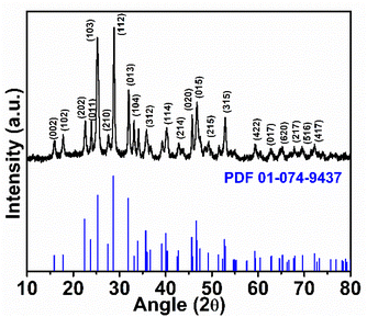
In the present work, Bi2S3 and FeS–Bi2S3 were synthesized via a template-free hydrothermal method.The XRD diffractogram of the as-synthesized Bi2S3, as shown in Fig. 1, reflects its crystalline nature and is consistent with its orthorhombic phase with the Pnma (62) space group. No other impurity crystal phases were observed. Fig. 2a shows the TEM micrograph of Bi2S3, which reveals the formation of ultrafine rods with a width of ∼22 nm and length of ∼300 nm. The high-resolution TEM image in Fig. 2b clearly indicates the single crystalline nature of the Bi2S3 nanorods. The adjacent lattice fringes in Fig. 2b show the interplanar spacing of 0.311 nm, which corresponds to the (112) plane of Bi2S3. The EDAX spectra show the presence of Bi and S together with Cu due to the carbon-coated copper grid.
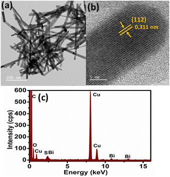 | ||
| Fig. 2 (a) TEM micrograph, (b) HR-TEM image and (c) electron dispersive spectroscopy (EDS) spectrum of Bi2S3 nanorods. | ||
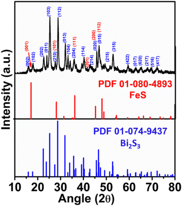
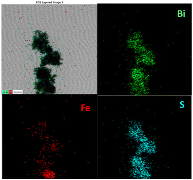
Given that Fe was introduced during the process for the synthesis of Bi2S3, FeS (mackinawite) was formed together with Bi2S3, leading to its decoration on Bi2S3, forming a heterostructure. Fig. 3 shows the XRD pattern of the as-formed FeS–Bi2S3 heterostructure, which majorly matches Bi2S3, together with overlapped planes of FeS (tetragonal, P4/nmm (129)). The TEM micrograph in Fig. 4a shows that FeS–Bi2S3 retained its morphology with the nanorods possessing a length of about 350 nm and width of 30 nm. The HR-TEM image in Fig. 4b shows the close contact of the formed phases with an interplanar distance of 0.351 nm, which corresponds to the (103) plane of Bi2S3, and an interplanar spacing of 0.278 nm, corresponding to the (110) plane of FeS. The EDAX spectrum of the FeS–Bi2S3 heterostructure in Fig. 4c shows the presence of Bi, Fe and S. The Cu peak originated from the carbon-coated Cu grid mesh. The atomic % (at%) of Bi, S and Fe in Bi2S3 and FeS–Bi2S3 is presented in Table S1.† The TEM-EDAX mapping in Fig. 5 shows the uniform distribution of Bi, Fe and S in the cluster of the formed nanorods of the heterostructure.
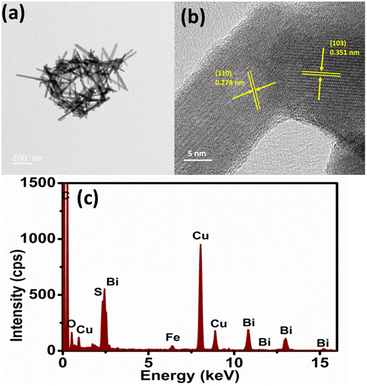 | ||
| Fig. 4 (a) TEM micrograph, (b) HR-TEM image and (c) electron dispersive spectroscopy (EDS) spectrum of FeS–Bi2S3 nanorods. | ||
The vibrational peaks in the Raman spectra of Bi2S3 appear at 116, 250, 415 and 968 cm−1 and FeS–Bi2S3 shows peaks at similar values together with one additional peak at 294 cm−1 (Fig. S1†). The Raman vibrational peak at 115 cm−1 can be assigned to the B3u phonon mode, which is inherently IR active but transforms to the Raman-active mode due to some defects originating from the lattice displacements in Bi2S3. The Raman-active Ag transverse in-plane vibration produced the peak at 250 cm−1. The other peak at 415 cm−1 matches well with the value reported in the literature by Sharma et al.27 The absorption peak appearing at 968 cm−1 is attributed to the surface phonons arising due to the high surface to volume ratio. In the spectrum of FeS–Bi2S3, the additional peak at around 300 cm−1 is the characteristic of the symmetric stretch in the FeS bonds in mackinawite.28
To gain insight into the surface composition and oxidation state of Bi2S3 and FeS–Bi2S3, they were examined by XPS, as shown in Fig. S2† and Fig. 6, respectively. The survey spectrum of Bi2S3 in Fig. S2† shows the presence of Bi and S. The narrow scan spectrum for Bi in Fig. S2(b and c)† shows two peaks centred at 163.28 and 158 eV, corresponding to Bi 4f5/2 and Bi 4f7/2, respectively. The spin–orbit coupling doublet of S 2p overlaps with the Bi 4f5/2 region in the narrow scan spectrum. The magnified XPS spectra for the S 2p core levels are shown just below the Bi 4f region in Fig. S2(c)† to effectively distinguish between them. The survey spectrum of FeS–Bi2S3 shows signals for Bi, S and Fe (Fig. 6(a)). The high-resolution XPS spectrum of Bi in Fig. 6(b) shows two dominant peaks at 158.18 and 163.48 eV, which correspond to the Bi 4f7/2 and Bi 4f5/2 spin states in FeS–Bi2S3.29 The Fe in FeS–Bi2S3 shows peaks at 710.1 and 723 eV, which refer to the spin states of the Fe 2p3/2 and Fe 2p1/2 core levels, respectively (Fig. 6(c)).30 Both Fe peaks in Fig. 6(c) correspond to the Fe2+ oxidation state, which indicates that the Fe in the FeS–Bi2S3 lattice is present in the form of FeS. No peaks of Fe in the +3 oxidation state were observed, which rules out the formation of other sulphide species such as Fe7S8 and Fe9S10. Two unsymmetric peaks appear for the S 2p core level region in FeS–Bi2S3. The signal for S 2p at 162.3 eV corresponds to S 2p3/2 and the peak at 160.8 eV refers to S 2p1/2.
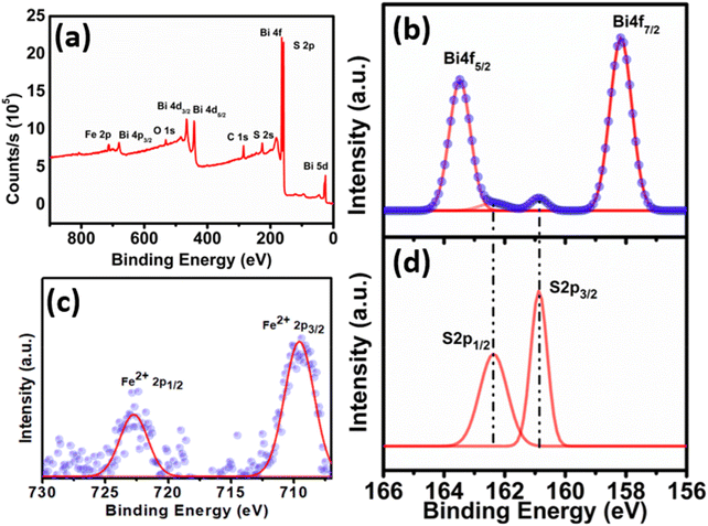 | ||
| Fig. 6 (a) XPS survey spectrum of FeS–Bi2S3 and high-resolution spectra of (b) Bi 4f, (c) Fe 2p and (d) S 2p. | ||
3.1. Field emission studies
Field emission is the quantum mechanical tunnelling phenomena whereby electrons traverse from the cathode, serving as the emitting material, across a vacuum barrier to the anode, propelled by a substantial electric field ranging from 106 to 107 V cm−1 generated by conducting or semiconductor materials. The distance between the cathode and anode is kept fixed at 200 μm. An increase in the aspect ratio and enhanced cathode sharpness, regardless of the material, lead to higher field emission currents. Nanostructures are believed to possess significant application potential in various areas, such as power tubes of microwaves, displays of flat panels, vacuum electronics and various other electron sources. Carbon nanotubes (CNTs) and other nanostructured materials share many advantageous properties and hold great promise for use in field emission (FE) applications. Nanostructured materials exhibit an extraordinarily high thickness to lateral size ratio, known as the aspect ratio. These nanomaterials have protruding and sharp active edges and immense defect sites, which can make electron tunnelling more likely, similar to that seen in carbon nanotubes.The variation in the emission current density of nanostructured semiconducting materials with a change in electric field is given by the modified Fowler–Nordheim (F–N) equation, as follows:
 | (1) |
Thus, the field enhancement factor (βFE) is defined as the ratio between the applied and local electric fields, which are distinct at the emission sites. The combined impact of the increase in local electric field is given by the slope (m) of the FN plot and work function (Φ) of the emitting material by the following equation:
 | (2) |
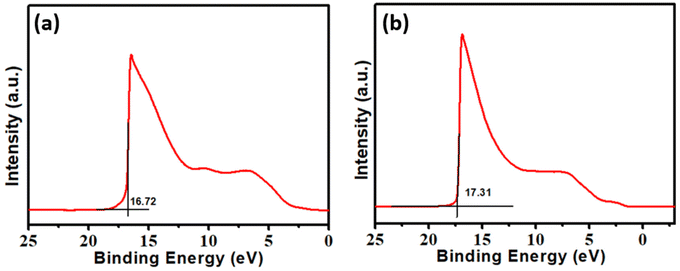
The amplification of the field enhancement effect, the promotion of electron entry into the vacuum via the tunnelling effect, and the improvement of the field emission performance of the emitter are all correlated with an increase in the value of β. Generally, the β values are related to the spatial distribution of the emission centres, vacuum intervals, crystalline structure, and emitter shape (including aspect ratio). In film field emission, each electron emission site may be regarded as a microtip, which requires a geometric field enhancement factor that can be computed based on the its dimensions. The FN theory posits that the field enhancement factor signifies the cumulative impact of all the emission microtips. The β value is determined by calculating the slope of the FN plot, specifically the natural logarithm of (J/E2) versus 1/E. The morphology, doping, type of defects, and concentration of defects in a material all affect its work function. The work function of a material greatly affects the current density of field emission. The quantum mechanical tunnelling process serves as the basis for determining the field emission current density from the Fermi energy. The work function (Φ) is defined as the difference between the constant vacuum energy level (Ev) and the Fermi level (Ef). The work function is calculated using ultraviolet photoelectron spectroscopy (UPS) as Φ = Evac − EF, where Evac represents the converged electrostatic potential in the vacuum region and EF denotes the Fermi energy, defined here as the valence band maximum (VBM). As shown in Fig. 7, the calculated values of the work function for Bi2S3 and FeS–Bi2S3 are 4.5 and 3.9 eV, respectively. The effect of an electric field on the field emission current density is proportional to its strength; E = V/d, where V is the applied voltage and d is the distance between the anode and the sample. Because of their high aspect ratio and the greatly improved local electric field anticipated at their edges, nanostructures exhibit qualities that are comparable to or even better than that of carbon nanotubes.
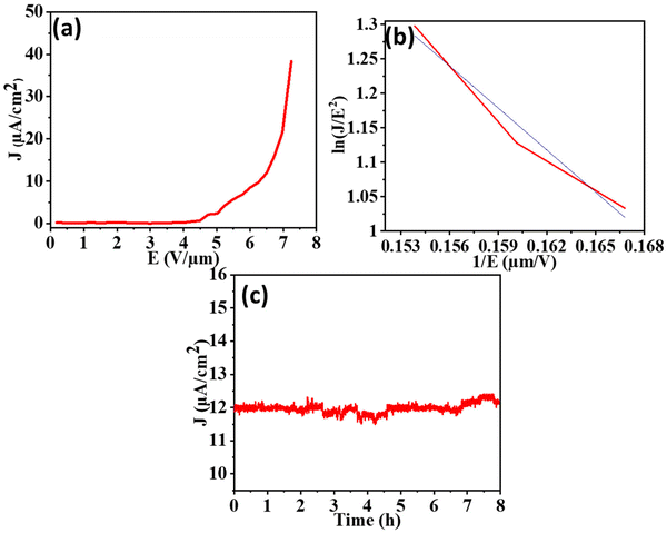
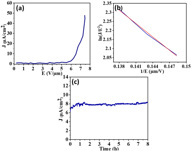
The field emission characteristics (Fig. 8a and 9a) demonstrate that the Bi2S3 emitter produced an emission current density of 38.3 μA cm−2 at an applied field of 7.2 V μm−1, whereas the FeS–Bi2S3 emitter produced an emission current density of 48 μA cm−2 at the field strength of 7.4 V μm−1. The nonlinearity observed in the emitters is a result of their semiconducting nature. This can be attributed to several factors, such as screening of the field amongst adjacent emission sites in the nanostructures, changes in their aspect ratio, penetration of field, band bending, and emission of other energy bands such as bands of metastable surfaces and conduction or valence bands. The F–N plot exhibits nonlinearity throughout the applied field range, which signifies that the emitter possesses semiconducting properties. The conduction band is where most electrons are released when there is a lower applied field. Alternatively, the electrons from the valence band tunnel out as the applied field increases, adding to the emission current.
The cold field emission mechanism is indicated by the negative slope of the straight line that fits the FN plot for both Bi2S3 and FeS–Bi2S3. The emitter shape, electrical characteristics, band structure, carrier mobility, crystal structure, surface characteristics, defects and vacancies are some of the variables that affect the density of the emission current. The two primary causes of the disparity in the current density between Bi2S3 and FeS–Bi2S3 are their morphology and crystal structure. The turn-on field refers to the minimum electric field required to provide a current density of 10 μA cm−2. The measured turn-on field values for Bi2S3 and FeS–Bi2S3 are 6.2 V μm−1 and 6.5 V μm−1, respectively. The lower value of the turn-on field meets the requirements for an improved field emitter.
The patterns of field emission current stability for the Bi2S3 and FeS–Bi2S3 nanorod field emitters at different set levels are shown in Fig. 8(c) and 9(c), respectively. The measurements were performed every 10 s over an 8 h period with an applied electric field of 12 V μm−1. Both Bi2S3 and FeS–Bi2S3 exhibited a consistent emission current density.
The field enhancement factor values for the Bi2S3 and FeS–Bi2S3 samples are approximately 3.1 × 10³ and 2.2 × 10³, as shown in Fig. 8(b) and 9(b), respectively. Table 1 displays the computed values of the field emission parameters.
| Sample | Turn-on field (V μm−1) at 10 μA cm−2 | Slope (eV) | True work function (eV) | Field enhancement factor (β-factor) | J max (μA cm−2) |
|---|---|---|---|---|---|
| Bi2S3 | 6.2 | −20.3 | 4.5 | 3.1 × 10³ | 38.3 |
| FeS–Bi2S3 | 6.5 | −24.6 | 3.9 | 2.2 × 10³ | 47.6 |
Materials with nanostructured surfaces, such as nanowires and nanorods, have higher field enhancement factors because of the localized electric fields at their tips. In the present case, surface modification of Bi2S3 by FeS to form the FeS–Bi2S3 heterostructure facilitated an enhancement in current density due to the ease of release of surface electrons by lowering the work function of FeS–Bi2S3 (3.9 eV). The slight decrease in the field enhancement factor for the FeS–Bi2S3 heterostructure is due to its dielectric screening effects and slightly lower aspect ratio (11.6), in which the local electric field is diminished due to polarization effects. The FeS–Bi2S3 heterostructure leads to charge redistribution, which will diminish the localized electric field, and thus the field enhancement factor. Thus, both the lowering of the work function and emitter morphology play deciding roles in the enhancement in current density.
The Bi2S3 and FeS–Bi2S3 nanostructure emitters demonstrated a consistent emission current density of 12 μA cm−2 and 8 μA cm−2, respectively, for a duration of 8 h. During the field emission (FE) measurement, the emitter surface is bombarded with ions, causing the gaseous species that are adsorbed onto or trapped between the nanostructures to be released.
The process of cleaning the emitter surface accounts for the enhancement in the emission current. The calculation of the current density fluctuation (cflu) was determined using the following formula:
 | (3) |
For continuous emission up to 8 h (t), the emission current density (J) recorded at a preset current value of 12 μA cm−2 and 8 μA cm−2 for Bi2S3 and FeS–Bi2S3 exhibited no discernible degradation, with minor current swings of ±3% for the average current values, respectively.
A consistent and steady flow of electric current is necessary for the potential advancement of field emitters in various technological applications. Fig. 8c and 9c display the stability of the field emission (FE) strategy of Bi2S3 and FeS–Bi2S3, respectively. The good electrical contact between the silicon substrate and Bi2S3 and FeS–Bi2S3 nanorods improves the FE current stability. This feature is remarkable, particularly in the context of an electron source application.
4. Conclusion
The present work demonstrated the simple, facile, template-free hydrothermal synthesis of Bi2S3 and FeS–Bi2S3 heterostructure. The TEM analysis showed the formation of nanorods with a length of 350 nm and width of 30 nm. The Raman spectral analysis confirmed the presence of the FeS (mackinawite) phase, together with the signature peak values of Bi2S3 in the spectrum of FeS–Bi2S3. The XPS analysis also ruled out the presence of any other oxidation states, ascertaining the presence of FeS in the heterostructure. Further, for the field emission studies, the samples were spin-coated on an Si wafer in the form of a thin film. Both Bi2S3 and FeS–Bi2S3 showed almost comparable values for the turn-on field but an enhanced current density value. The field enhancement factor was found to be 2.2 × 10³ for FeS–Bi2S3 and 3.1 × 10³ for Bi2S3. The introduction of FeS in Bi2S3 considerably lowered the work function of Bi2S3 from 4.5 eV to 3.9 eV, together with an enhancement in its current density. The introduction of metal sulphides of earth abundant metals such as Fe opens wider prospects for the inclusion of other earth abundant metal ion heterostructures in Bi2S3 for studying their field emission properties.Data availability
Data will be made available upon request.Conflicts of interest
There are no conflicts of interest to declare.Acknowledgements
All authors thank INST Mohali, DST and IIT Delhi for providing infrastructure support. AA and NK thank INST Mohali for fellowship support. AM gratefully acknowledges financial support from PMRF, Govt. of India. SG would like to acknowledge DST/TDT/DDP-52/2021 project for research support in present work.References
- G. Shen and D. Chen, Front. Optoelectron. China, 2010, 3, 125–138 CrossRef
.
- V. Autade, S. Tekale, R. Kate, C. Mistari, M. More, S. Apte and B. Kale, Mater. Sci. Eng., B, 2023, 296, 116683–116692 CrossRef CAS
.
- P. W. Dunne, C. L. Starkey, M. Gimeno-Fabra and E. H. Lester, Nanoscale, 2014, 6, 2406–2418 RSC
.
- Y. Liu, M. Li, Y. Zheng, H. Lin, Z. Wang, W. Xin, C. Wang and F. Du, Nanoscale, 2020, 12, 24394–24402 RSC
.
- J. L. Liu, H. Chen, X. Li, H. Wang, Z. K. Zhang, W. W. Pan, G. Yuan, C. L. Yuan, Y. L. Ren and W. Lei, J. Alloys Compd., 2019, 798, 656–664 CrossRef CAS
.
- J. L. Liu, H. Wang, X. Li, H. Chen, Z. K. Zhang, W. W. Pan, G. Q. Luo, C. L. Yuan, Y. L. Ren and W. Lei, J. Alloys Compd., 2019, 798, 656–664 CrossRef CAS
.
- F. Urban, M. Passacantando, F. Giubileo, L. Iemmo and A. Di Bartolomeo, Nanomaterials, 2018, 8, 1–10 Search PubMed
.
- P. K. Bankar, L. N. Khandare, D. J. Late and M. A. More, ChemistrySelect, 2017, 2, 10912–10917 CrossRef CAS
.
- A. Mahajan, N. Khan, K. K. Yadav, M. Jha and S. Ghosh, Appl. Surf. Sci., 2023, 623, 156996 CrossRef CAS
.
- Y. Feng, E. Du, S. Gong, K. Yu, X. Chen and Z. Zhu, CrystEngComm, 2020, 22, 3797–3803 RSC
.
- S. Mishra, P. Yogi, S. K. Saxena, J. Jayabalan, P. Behera, P. R. Sagdeo and R. Kumar, J. Mater. Chem. C, 2017, 5, 9611–9618 RSC
.
- Y. Yu, C. H. Jin, R. H. Wang, Q. Chen and L.-M. Peng, ChemInform, 2005, 36, 18772–18776 Search PubMed
.
- B. Chitara, B. S. C. Kolli and F. Yan, Chem. Phys. Lett., 2022, 804, 139876 CrossRef CAS
.
- L. Zhang, S. Hou, P. Li, S. Zhou, S. Zhang and H. Li, Colloids Surf., A, 2021, 618, 126397 CrossRef CAS
.
- T. O. Ajiboye and D. C. Onwudiwe, Results Chem., 2021, 3, 100151 CrossRef CAS
.
- L. Jun, M. Junfeng, Y. Yan, R. Yang, L. Botao, J. Xiaohui, S. Yong, F. Jingrui and L. Zhensen, J. Am. Ceram. Soc., 2008, 91, 2425–2428 CrossRef
.
- T. O. Ajiboye, A. A. Mafolasire, S. Lawrence, N. Tyhali and S. D. Mhlanga, J. Inorg. Organomet. Polym. Mater., 2023, 34, 433–457 CrossRef
.
- M. Medles, N. Benramdane, A. Bouzidi, A. Nakrela, H. Tabet-Derraz, Z. Kebbab, C. Mathieu, B. Khelifa and R. Desfeux, Thin Solid Films, 2006, 497, 58–64 CrossRef CAS
.
- Z. H. Ge, B. P. Zhang, Z. X. Yu and B. Bin Jiang, CrystEngComm, 2012, 14, 2283–2288 RSC
.
- H. Wang, R. Liu, S. Zhang, Y. Wang, H. Luo, X. Sun, Y. Ren and W. Lei, Opt. Mater., 2022, 134, 113174 CrossRef CAS
.
- X. Yu and C. Cao, Cryst. Growth Des., 2008, 8, 3951–3955 CrossRef CAS
.
- T. Ganesh, J. Lee, R. S. Mane, W. K. Yi, B. N. Pawar, B. Won Cho and S. H. Han, J. Appl. Phys., 2008, 103, 1–4 Search PubMed
.
- L. Zhang, X. Liu, Z. Lian, X. Wang, G. Shen, D. Shen and Q. Yan, J. Mater. Chem. C, 2014, 2, 3965–3971 RSC
.
- M. Sreekanth, P. Srivastava and S. Ghosh, Appl. Surf. Sci., 2020, 508, 145215 CrossRef CAS
.
- M. Sreekanth, S. Ghosh, P. Biswas, S. Kumar and P. Srivastava, Appl. Surf. Sci., 2016, 383, 84–89 CrossRef CAS
.
- S. Saini, S. Ghosh and P. Srivastava, Appl. Surf. Sci., 2023, 635, 157653 CrossRef CAS
.
- S. Sharma and N. Khare, Adv. Powder Technol., 2018, 29, 3336–3347 CrossRef CAS
.
- E. B. Hansson, M. S. Odziemkowski and R. W. Gillham, Corros. Sci., 2006, 48, 3767–3783 CrossRef CAS
.
- E. Miniach and G. Gryglewicz, J. Mater. Sci., 2018, 53, 16511–16523 CrossRef CAS
.
- A. Nigam and S. Kala, Mater. Today: Proc., 2022, 66, 2144–2151 CAS
.
Footnote |
| † Electronic supplementary information (ESI) available. See DOI: https://doi.org/10.1039/d4nr04138k |
| This journal is © The Royal Society of Chemistry 2024 |

